Abstract
Organometallic halide perovskite (PVK)-based solar cells (PSC) have gained significant popularity owing to their efficiency, adaptability, and versatility. However, the presence of lead in conventional PVK poses environmental risks and hinders effective commercialization. Although lead-free PVK solar cells have been developed, their conversion efficiency is limited due to intrinsic losses. To address this challenge, we present a simulation study focusing on methylammonium tin bromide (MASnBr3) as an alternative material. In our investigation, the MASnBr3 layers are strategically placed between a copper iodide (CuI)-based hole transporting material (HTM) and a zinc oxide (ZnO)-based electron transporting material (ETM). We optimize the active layer thickness, operating temperature, defect density analysis, and series resistances to assess device performance. Furthermore, we employ contour mapping, considering both thickness and defect density, for a detailed investigation. Our primary objective is to achieve unprecedented efficiency in lead-free MASnBr3-based PSCs. Remarkably, our study achieves the highest JSC (short-circuit current density) of 34.09 mA/cm2, VOC (open-circuit voltage) of 1.15 V, FF (fill factor) of 82.06%, and optimized conversion efficiency of 32.19%. These advancements in conversion efficiency pave the way for the development of lead-free PVK solar cells in the desired direction.
1. Introduction
Scientists have been actively working on enhancing the efficiency (η) of solar cells as a clean and pollutant-free alternative to traditional fossil fuels. Among the various types of solar cells, perovskite solar cells (PSC) have gained significant attention due to their exceptional properties. These properties include higher absorbance value, cost-effectiveness, extended charge diffusion, improved carrier mobility, lower trap density, lower binding energy, and variable band gaps [1,2,3,4,5]. The pioneering work by Kojima et al. introduced the noble structure of PSC. They demonstrated that by using CH3NH3PbX3 as the halide material to form the active layer, the power conversion efficiency (PCE) of PSC could be enhanced up to 3.8% [6]. Despite significant advancements in PSC performance over the years, there is still ample room for further research and development. To improve the efficiency of these devices, careful selection of materials and ideal thicknesses in device design is crucial. Because active layers are often thin and absorb more photons than other layers, the PSC offers a smaller photocurrent density. However, increasing the thickness of the active layer leads to losses associated with recombination, as a thicker perovskite active layer hinders efficient charge extraction [7,8,9,10].
In the conventional design of perovskite solar cells (PSC), the perovskite layer is positioned between the hole transport layer (HTL) and the electron transport layer (ETL). The efficiency of PSCs was improved by incorporating titanium dioxide (TiO2) as the ETL and applying an annealing treatment, resulting in an enhancement of up to 6.5% [11]. To further enhance effectiveness and stability, Kim et al. simultaneously employed Spiro-OMeTAD as the HTL [12]. Another study conducted by Liu et al. demonstrated a significant efficiency improvement of 15.4% by utilizing a complex device structure consisting of ITO/TiO2/CH3NH3PbI3−xClx/Spiro-OMeTAD/Ag layers [13]. However, Spiro-OMeTAD is relatively expensive compared to other HTL materials. In our simulation study, we employed copper iodide (CuI) as the HTL for the entire experiment due to its cost-effectiveness. Additionally, Xi et al. provided theoretical insights into improving efficiency by incorporating graphene in solar devices [14]. It is important to highlight the significance of planar heterojunction perovskite solar cells, which have emerged as a viable alternative to mesoscopic counterparts. The simplified structure and straightforward manufacturing process of planar heterojunction PSCs offer a more accessible and practical approach to harnessing solar energy, avoiding the complexities and intricate fabrication techniques associated with mesoscopic designs [15]. However, it is important to note that achieving perfect optoelectronic properties in the light-harvesting layers, devoid of any defects, has a significant impact on the overall performance of PSC devices. Defects in the perovskite material can hinder the efficient absorption of light and charge transport, leading to lower device-level outputs such as reduced photocurrent and lower power conversion efficiency. Therefore, mitigating defects and improving the optoelectronic properties of the light-harvesting layers are crucial for maximizing the performance and output of perovskite solar cells [16,17,18]. Although there have been significant advancements in lead-based perovskite materials over recent few decades, lead toxicity remains a significant barrier to the broad use of PSCs [19,20]. These issues can be resolved by substituting Sn for Pb, which offers improved stability and non-toxicity [21,22,23]. MASnBr3 is a substitute material with a bandgap of nearly 1.3 eV and a significantly smaller band gap than conventional perovskite (PVK) material [24,25,26]. Having a lower bandgap, MASnBr3 can absorb a photon’s wavelength up to a wider range; therefore, it can improve efficiency. Almost all the available technology computer-aided design (TCAD) tools for solar cell simulation are equipped with basic semiconductor equations to solve the optoelectronic performance. However, SCAPS-1D is user-friendly and open source, and the same is validated through extensive publications of the article on solar cell simulation using a 1-D solar cell capacitance simulator developed by ELIS, University of Ghent, Ghent, Belgium SCAPS-1D [27]. In the present work, MASnBr3 has been used to design and simulate PSC using SCAPS-1D; it is primarily preferred in recent years for the investigation of perovskite solar cells where the drift-diffusion model was functionalized [28]. The simulator offers unique advantages, including the power to deposit up to seven semiconducting layers and the ability to grade virtually all characteristics. The computation process is based on solving the Poisson and continuity equations, and the simulations may be done in both dark and light conditions [29,30]. Apart from the above aspects, the simulator is suitable for easily analyzing various design models with recombination kinetics, batch computation with bulk, and interface defect-level calculation [31,32]. Additionally, the present simulation may be used for both crystalline and amorphous solar cells.
In this study, we employed AM1.5G solar illumination to compute the optical profile, which can be translated to the electrical modeling for MASnBr3-based PSCs to evaluate the carrier transport phenomena and electrical outputs. The lead-free material in the solar cell can be appreciated for non-toxicity issues as well as better stability. In comparison to the MASnI3 material, the bromine-based MASnBr3 material has been found to offer higher efficiency in perovskite solar cells. So, the selection of MASnBr3 material for designing a PSC device is done. Moreover, the thorough study in the lead-free PSC can be better for future optimization of the devices. The selection of other constituent layers in the PSC devices are from earlier published works [5,33]. Furthermore, the selection of CuI as the HTM is also considered as one of the better approach to replace the expensive and most commonly used HTM of Spiro-OMeTAD. Moreover, the main aim is to achieve the efficiency near to the Shockley–Queisser limit. The current simulation exclusively try to deal with the mentioned problems. The comprehensive computational study of MASnBr3-based PSC combines temperature dependence, defect-free methodology, and PVK material optimization. For PVK-based PSC structures, such as MASnBr3, the key solar cell metrics, such as short circuit current density (JSC), open-circuit voltage (VOC), fill factor (FF), and power conversion efficiency (PCE), are also observed in suitable conditions. Additionally, to enhance the interpretation of the simulation results, the study and comparison with earlier work is also provided in the result sections to elucidate the scientific implications.
2. Simulated Device Structures
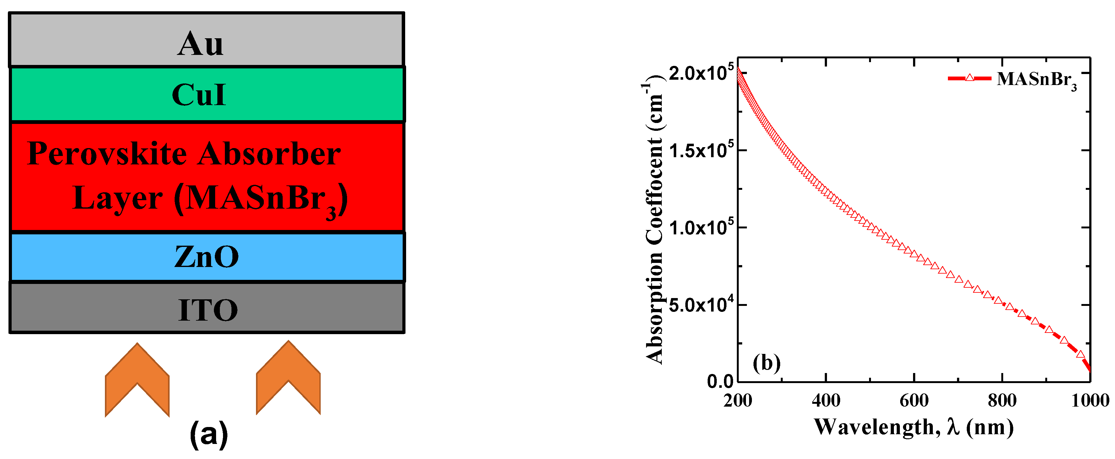
To simulate the proposed PSC devices, heterojunction PSCs with the ITO/ZnO/MASnBr3/CuI/Au device configuration have been designed, as shown in Figure 1a. At the same time, the 0.1-µm thick ZnO layer is the ETL, which effectively gathers electrons from MASnBr3 absorber layers in the PSC architecture—similarly, 1 µm ITO top electrode in the simulated PSC devices. The absorber layer for the devices has a 100 µm thickness, and it is retained between an HTL and an ETL. From the absorber layer, the carriers are successfully collected and transferred to the cathode by the drift-diffusion mechanism. The thickness of the CuI is 0.1 µm, and the cathode of Au material has a thickness of 0.1 µm. The parameters utilized in the PSC device simulation are shown in Table 1. At the same time, the absorption coefficient of MASnBr3 has been obtained from SCAPS-1D software for use as the absorber in the PSC device, as shown in Figure 1b. Moreover, Figure 1c depicts the energy levels of all the constituent layers in the PSC device [33,34,35]. While Table 1 and Table 2 shows the inputs used in the simulation that is validated from the mentioned published work.
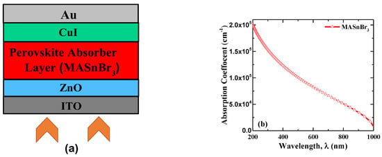
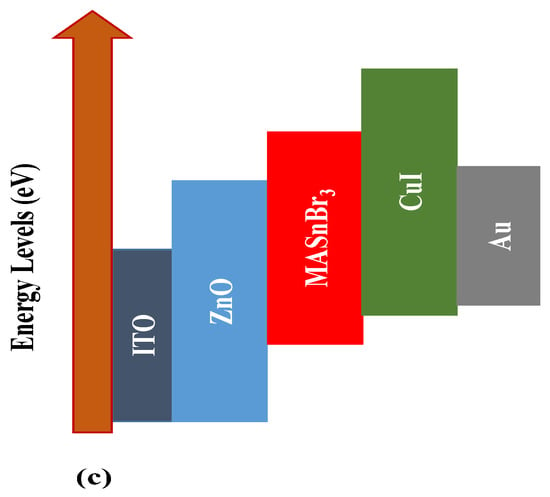
Figure 1.
(a) The design of MASnBr3-based PSC device, (b) the absorption coefficient of MASnBr3 material, and (c) energy levels of the constituent layers.

Table 1.
The simulated parameters in the architecture of the simulating device [5,33,34].

Table 2.
Parameter of interface defects used in simulations.
3. Computational Modeling
The utilization of computational simulation approaches plays a crucial role in elucidating and simplifying the underlying principles governing solar devices, including perovskite solar cells. Numerical modeling offers a cost-effective and time-efficient alternative to traditional trial-and-error approaches in solar cell development. Building and testing physical prototypes can be expensive, time-consuming, and resource-intensive. Furthermore, computational simulations facilitate the identification and understanding of complex phenomena that may not be easily observed or measured experimentally.
The computational simulation approach plays a crucial role in understanding and simplifying the underlying principles governing solar devices. By examining how various basic factors influence the optimal output of these devices, numerical modeling becomes essential. Without such simulations, the practicality of building a solar cell is compromised, leading to increased costs and longer lead times [35,36]. Over time, numerical simulation has gained significance, particularly in material science research [37]. The one-dimensional (1-D) equation governs the steady-state behavior of semiconductor materials. It helps establish the correlation between the electric fields (E) and the charge density of the p-n junction, as illustrated below: [7,38].
∂2φ/∂x2 = −∂E/∂x = −ρ/εs = −q·[p − n + ND+(x) − NA−(x) ± Ndef(x)]/εs,
In this context, the symbol φ represents the electrostatic potential, while q refers to the charge. The term εs corresponds to the static relative permittivity of the medium. The symbols n and p represent the electrons and holes, respectively, within the system. Additionally, NA− and ND+ denote the density of acceptors and donors, respectively. Lastly, Ndef represents the defect density encompassing both acceptors and donors.
In the context of the PSC structure, the carrier continuity equations and current density equations are as follows:
The carrier continuity equations describe the conservation of charge carriers (electrons and holes) in the semiconductor material. These equations express how the carrier concentrations change over time and space due to carrier generation and recombination processes.
For hole density (jp) and electron density (jn), the continuity equations are given by [29]:
where
−∂jp/∂x + G − Up(n,p) = 0
∂jn/∂x + G − Un(n,p) = 0
jp is the hole current density,
jn is the electron current density,
G is the carrier generation rate,
Up(n,p) is the recombination rate of holes, and
Un(n,p) is the recombination rate of electrons.
The current density of both carriers (holes and electrons) in the PSC can be obtained from the carrier mobility and carrier concentration gradient, which can be written as:
where
jp = qpμpE − qDp∂p/∂x
jn = qnμnE + qDn∂n/∂x
qp is the charge of a hole (positive charge),
qn is the charge of an electron (negative charge),
μp and μn are the hole and electron mobilities, respectively,
E is the electric field,
Dp and Dn are the diffusion coefficients of holes and electrons, respectively, and
∂p/∂x and ∂n/∂x are the spatial gradients of the hole and electron concentrations, respectively.
Typically, the SCAPS-1D simulator is capable of extracting essential equations related to solar cell operation, including recombination rate, generation rate, and current density.
4. Results and Discussions
4.1. The Alignment of the Bandgap of PSC
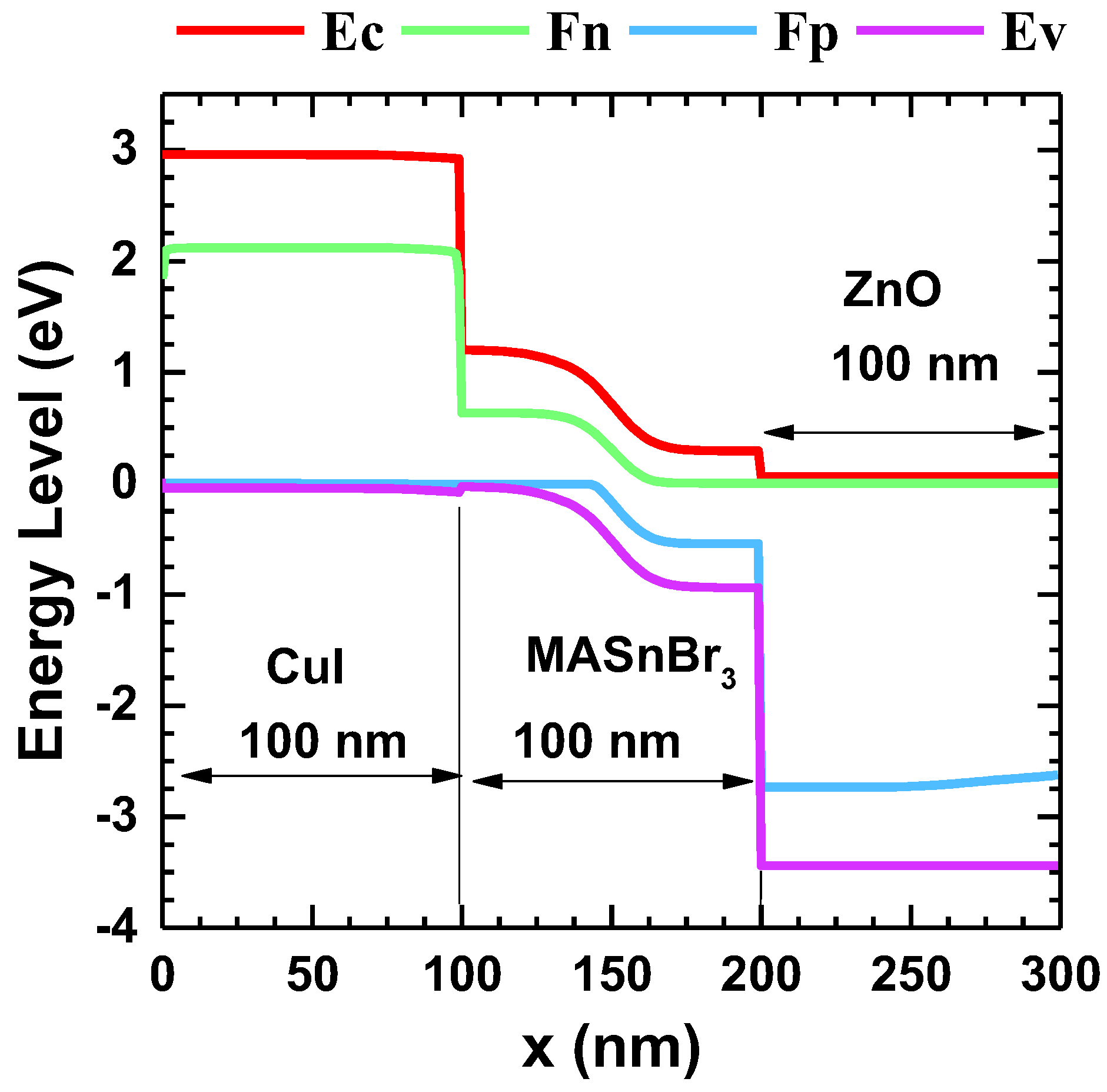
To check the band alignment of the PSC, we carried out the simulation at 300 K temperature and obtained the desired outcomes. The bias voltage of 2 V is used in the PSC simulation. Figure 2 shows the band diagram for the equilibrium simulated PSC devices. The calculation shows that the MASnBr3-based PSC device provides a very smaller value of energy barrier, nearly 0.2 eV, between the conduction band minima (EC) of ZnO and the lowest unoccupied molecular orbit (LUMO) of absorber material. In contrast, a high value of offset of nearly 1.92 eV between the highest occupied molecular orbit (HOMO) of the absorber material and HTL layer has been obtained. For MASnBr3-based PSC, the movement of electrons can be shown from the CB’s higher energy level to the ETL’s lower energy of CB, which can be understood from Figure 2.

Figure 2.
The energy band diagrams of MASnBr3-based PSC device.
4.2. Effect of Active Layer Thickness
It can be noted that thickness optimization of the constituent layer of the PSC is one of the most promising and effective techniques to optimize the PSC device’s efficiency. Through careful control of the perovskite layer thickness, researchers can enhance light absorption, improve charge carrier transport, reduce recombination losses, optimize interface properties, and achieve stable and reproducible device performance. This optimization process contributes significantly to the advancement of perovskite solar cell technology and its potential as a low-cost and efficient renewable energy source. The thickness of the PSC was increased from 0.2 µm to 1.6 µm and checked the compatible thickness for optimized efficiency of the simulated device.
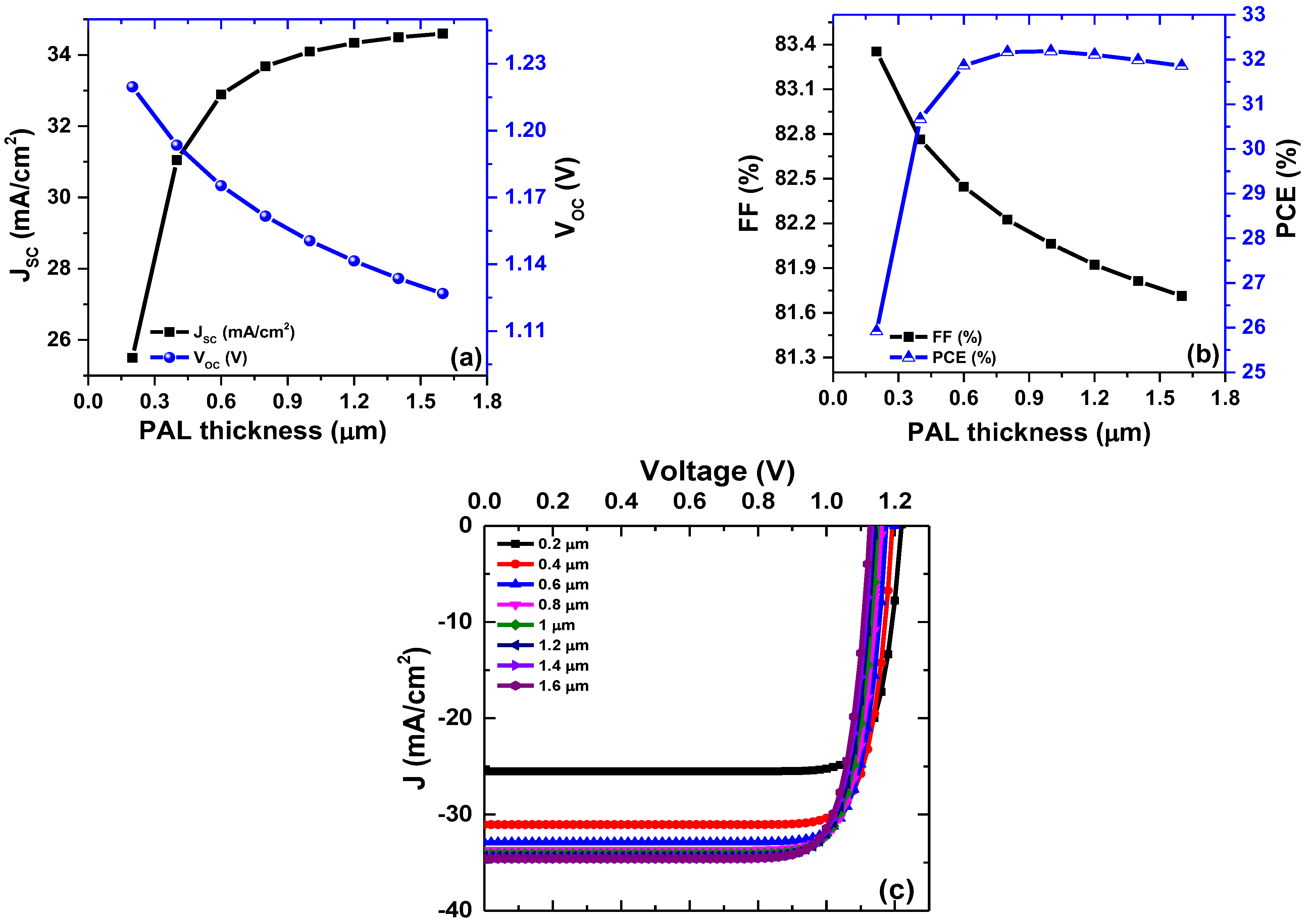
We investigated the impact of active layer thickness, specifically the perovskite-absorbing layer (PAL), on the output characteristics of perovskite solar cells (PSCs) using Sn-based materials using the input parameters of the materials from Table 1 and Table 2 and performed simulations or experiments at a temperature of 300 K. The influence of PAL thickness with that of the electron transport layer (ETL) and hole transport layer (HTL) was compared and found that PAL thickness had a more significant effect on the device’s performance. One key parameter that was analyzed is the short-circuit current density (JSC), which represents the maximum current density a PSC can generate under short-circuit conditions. The authors observed that as the PAL thickness increased, the JSC of the PSC devices also increased (Figure 3a). This suggests that a thicker PAL enables better light absorption and more efficient generation of electron-hole pairs within the device. Interestingly, the authors noted that the increase in JSC reached a saturation point at a PAL thickness corresponding to a JSC value of 34.3 mA/cm2. Beyond this optimal thickness, further increases in PAL thickness did not result in a significant improvement in JSC. This saturation might be attributed to factors such as enhanced charge carrier recombination or the PAL reaching a point of maximum light absorption. We further explained that the reason for the increase in JSC with increasing PAL thickness could be attributed to the proportional dependency between absorption rate and current density, as referenced in papers [19,22]. While the exact context and details of these references are not provided, this relationship suggests that the rate at which light is absorbed by the PAL is directly linked to the resulting current density. Therefore, as more light is absorbed due to an increase in PAL thickness, the current density, represented by JSC, also increases. By examining the impact of PAL thickness on JSC, the authors have demonstrated the importance of optimizing the active layer thickness in Sn-based PSCs. The findings emphasize the significance of PAL thickness as a critical design parameter for achieving high device performance. Thus, this study provides insights into the effect of active layer thickness, specifically the PAL, on the output characteristics of Sn-based perovskite solar cells. The observed increase in JSC with PAL thickness highlights the importance of light absorption in achieving higher current densities. Further investigations and analysis beyond the information provided, such as the mechanisms underlying the proportional dependency between absorption rate and current density, would offer a more comprehensive understanding of the observed phenomena and their implications for optimizing PSC performance.
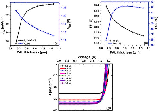
Figure 3.
(a,b) The four PSC parameters and (c) J–V characteristics for perovskite solar cell device structure at optimized preconditions.
We further investigated the variation in open-circuit voltage VOC with respect to the active layer thickness (perovskite-absorbing layer, PAL) in the range of 0.2 µm to 1.6 µm for Sn-based PSCs. The open-circuit voltage is an essential parameter that represents the maximum voltage a solar cell can achieve in the absence of an external load. It reflects the energy difference between the electron and hole quasi-Fermi levels in the device. The authors observed that as the PAL thickness increased, the VOC of the PSCs decreased monotonically (Figure 3a). This means that thinner PALs led to higher open-circuit voltages, while thicker PALs resulted in lower open-circuit voltages. One of the main reasons behind this behavior is an increase in carrier recombination rates within the PSC with increasing PAL thickness. Carrier recombination refers to the process where electrons and holes recombine, leading to the loss of charge carriers and reduced current in the device. As the PAL becomes thicker, the distance for charge carriers to travel within the active layer also increases. This leads to a higher probability of carrier recombination events, which negatively impacts the open-circuit voltage. Numerically, this study found that a 0.2 µm thick PAL resulted in the highest value of VOC, around 1.22 V, while a thicker PAL of 1.6 µm yielded a smaller VOC, approximately 1.125 V. These results suggest that there is an optimal PAL thickness that maximizes the open-circuit voltage in Sn-based PSCs. Beyond this optimum, further increasing the PAL thickness leads to increased recombination and reduced open-circuit voltage. Furthermore, the authors compared their findings with a reference study by Islam et al. [34]. It is noted that the present work offers a much higher value of open-circuit voltage than the mentioned reference. This indicates the significance of their study’s results and the potential for achieving higher device performance by optimizing the active layer thickness in Sn-based PSCs. The investigation into the variation in open-circuit voltage with active layer thickness provides valuable insights into the design considerations for improving PSC efficiency. The findings emphasize the importance of balancing charge carrier transport and recombination processes within the device by carefully controlling the thickness of the perovskite-absorbing layer. Additionally, the comparison with a previous study highlights the novelty and potential impact of the current work in the field of perovskite solar cells. Further discussions on the underlying physical mechanisms responsible for the observed trends and a deeper analysis of the implications of the optimal PAL thickness would enhance the results and provide a comprehensive understanding of the device behavior.
In Figure 3b, the device’s Fill factor (FF) property is depicted. The Fill factor shows the compatibility of the device. The FF decrease is from 83.44% to 81.7% while increasing the thickness of the absorber layer from 0.2 µm to 1.6 µm. The PCE value keeps increasing with thickness from 0.2 µm to 0.8 µm and reaches a maximum for thickness of 0.8 µm. After that, the PCE starts to decrease due to the combined impact of JSC, VOC, and FF. Apart from that, the higher efficiency of the PSC may be attributed to the smaller bandgap of MASnBr3, which is likely to enhance the electron-hole generation rate and contribute to the conductivity of the PSC. The present simulation is also significant for its non-toxicity as well as for obtaining higher efficiency. For comparison, the efficiency of the current finding is significantly higher than that of the earlier reports by Du et al. and Bhattarai et al. [19,21]. Figure 3c shows the combination of J–V characteristics for the PSC device. It can be observed that a much better value of JSC value is saturated at the thickness higher than 1 µm of the PSC device.
4.3. Effect of Temperature
In the simulation, the SCAPS-1D solves three different equations to account for the effect of temperature on material properties. According to Equations (6) and (7), the density of states in the conduction/valence band [NC(T)/NV(T)] varies with temperature. The thermal velocity vth(T) also depends on temperature, per Equation (8). Other parameters are assumed to remain constant regardless of temperature changes. The diffusion coefficient, which is used in the calculations, is temperature dependent and is given by D = μkT/q. The default temperature, T0, is set to 300 K in SCAPS and should be defined at this temperature [33].
NC(T) = NC(T0) · (T/T0)^(1.5)
NV(T) = NV(T0) · (T/T0)^(1.5)
vth(T) = vth(T0) · (T/T0)^(1.5)
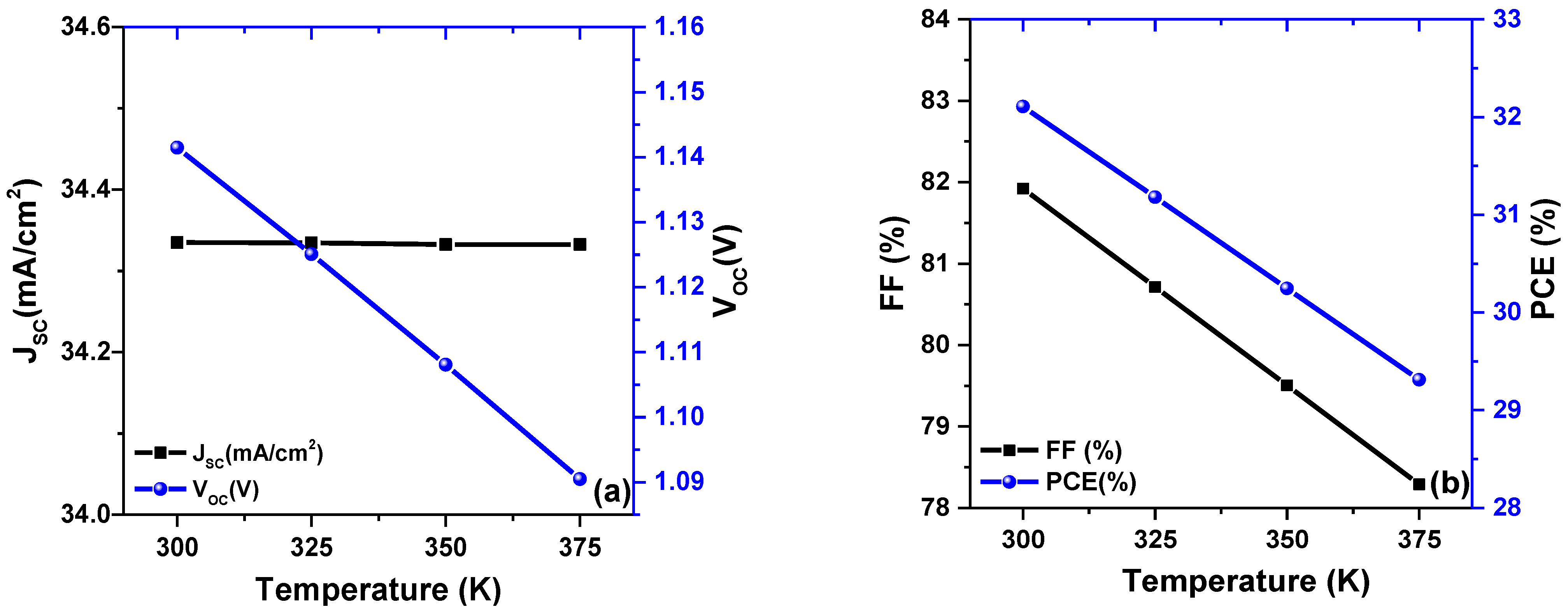
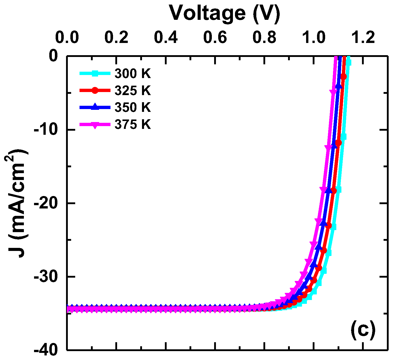
An increase in temperature increases all the three parameters, such as NC(T), NV(T) and vth(T), and the observed performance can be linked with the same. An increase in the density of states provided more states for the electrons and holes to occupy. However, the performance of a solar cell can also be affected by temperature-dependent thermal velocity because it influences the diffusion of carriers in the material. An increase in temperature has a direct impact on the thermal velocity of carriers (as described by Equation (8)), which refers to the speed at which carriers move within the material. As temperature rises, the thermal velocity of carriers also increases. This, in turn, can have adverse effects on the performance of the solar cell. This further leads to higher reverse saturation current (I0) and reduces the device performance, particularly in terms of VOC and FF, as shown in Figure 4a,b. Additionally, due to the temperature dependence of I0, the overall VOC experiences a linear decrease as the open-circuit voltage is affected by changes in temperature.
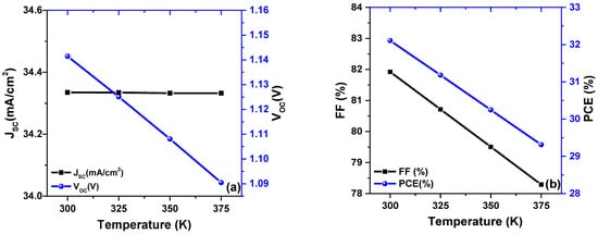
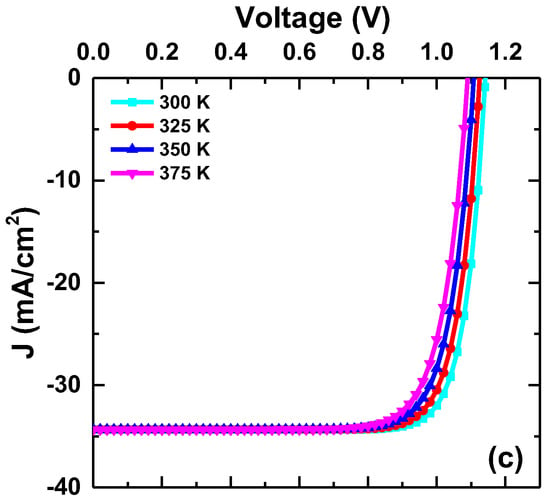
Figure 4.
The photovoltaic parameters, (a) JSC and VOC, (b) FF and PCE, and (c) J–V characteristics for different temperatures of the PSC structure.
Figure 4a,b illustrates the comprehensive analysis of solar cell properties concerning temperature fluctuations. The four parameters, JSC, VOC, FF, and PCE decreases as the temperature increases from 300 K to 375 K, which can be seen from the below observation. A maximum value of 34.335 mA/cm2 at 300 K is shown in the Jsc for the MASnBr3-based PSC devices, respectively. The primary dominant value of the Voc impacts the entire efficiency of the MASnBr3-based PSC devices—the reverse saturation current increases exponentially with an increase in temperature, which lowers VOC. As the highest VOC is 1.15 V at 300 K, it keeps on decreasing with an increase in the temperature and reaches a value of 1.09 V. While FF is highest for MASnBr3-based PSC devices at 300 K, achieving around 81.75%, its value decreases and drops to a minimum of 78.25%. Finally, it is evident that the maximum PCE is attained at 300 K, reaching levels of 32.19%.
On the other hand, the J–V curve is shown in Figure 4c, and it can be well observed that the temperature is more dominant on the VOC than the JSC value. The J–V characteristics also match with recent work by Du et al. and Singh et al. [21,39]. The exact value of the results is listed in Table 3.

Table 3.
Comparing the photovoltaic (PV) parameters of the simulated device with those obtained from previous research.
4.4. Effect of the Bulk Defect—Density of the Active Layers
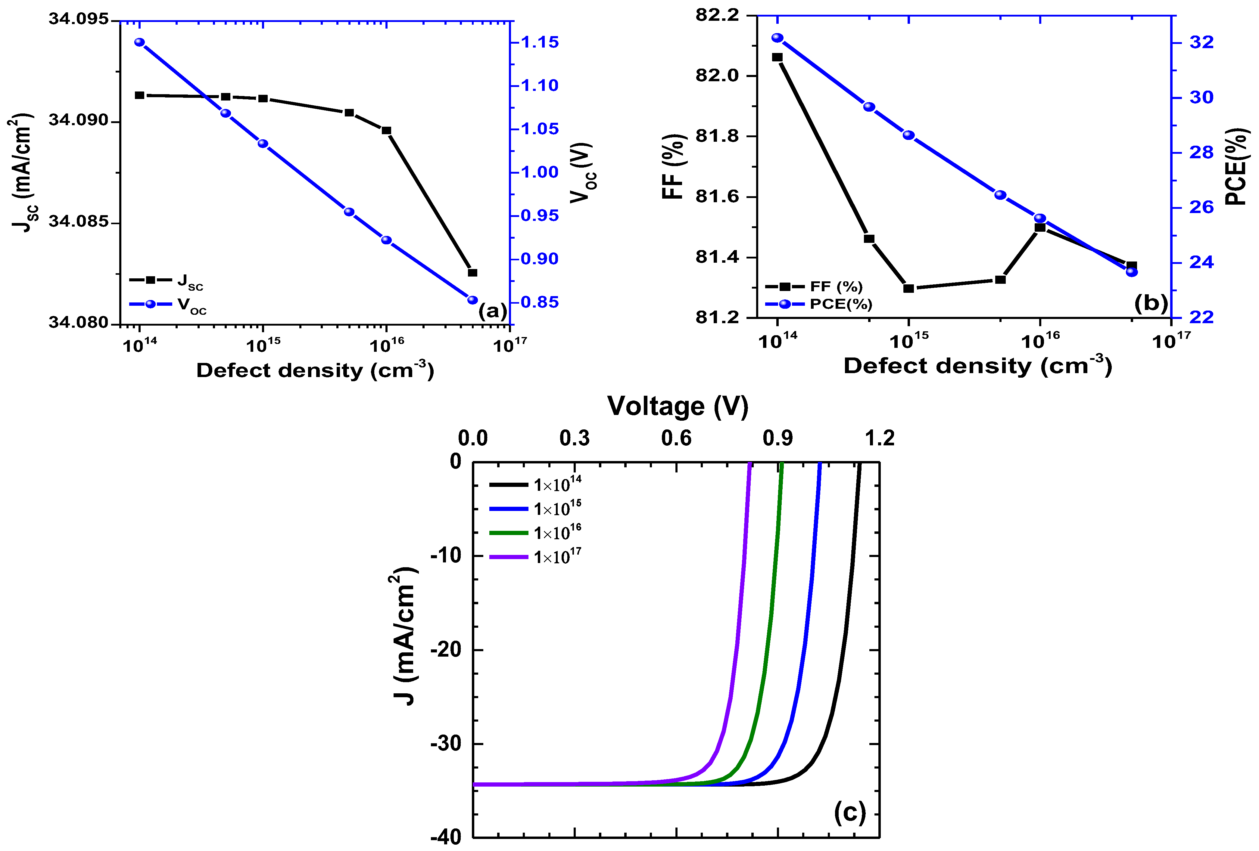
Figure 5 illustrates the impact of the defect densities on the simulated device architectures for eight bulk defect densities, which vary from 1 × 1014 cm−3 to 1 × 1017 cm−3. The value of PCE keeps dropping until it reaches a minimum value at the defect density level of 1 × 1017 cm−3. Numerically, As we can see that PCE drops from 32.19% to 23.72%; when we change the defect density from 1 × 1014 cm−3 to 1 × 1017 cm−3. The range of different defect density shows the significant change in PCE. However, experimentally, the suitable defect density can help in obtaining better efficiency of the solar cell. For this particular work, a defect density level of 1 × 1014 cm−3 can be used as most optimized condition of the PSC device. Changing the defect density below 1 × 1014 cm−3 shows no noticeable output differences in the PSC. It can be achieved that the MASnBr3-based material delivers the maximum JSC of 34.091 mA/cm2 for lower defectivity of the PSC. The lowest defectivity achieves the greatest VOC of 1.15 V, which keeps decreasing and reaches the smallest VOC of 0.81 V. The present simulation achieves a higher value of JSC than the previous study by Singh et al. [39]. This is understandable as the J–V parameter has an inverse relationship with defectivity, meaning that as defect density increases, the PSC’s effectivity decreases, as depicted in Figure 5.
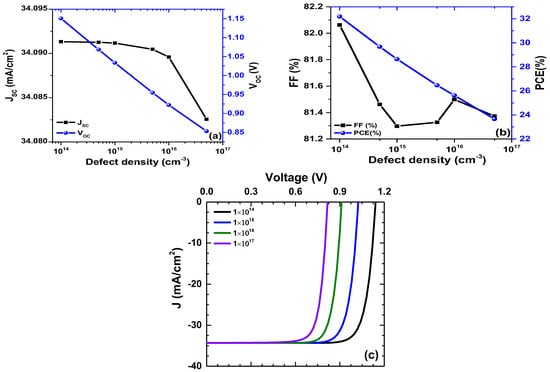
Figure 5.
Comparison of photovoltaic parameters, (a) Jsc and Voc, (b) FF and PCE and (c) J–V characteristics for MASnBr3-based PSC over different absorber total defect density.
4.5. Impact of Series Resistance on Outputs of the PSC
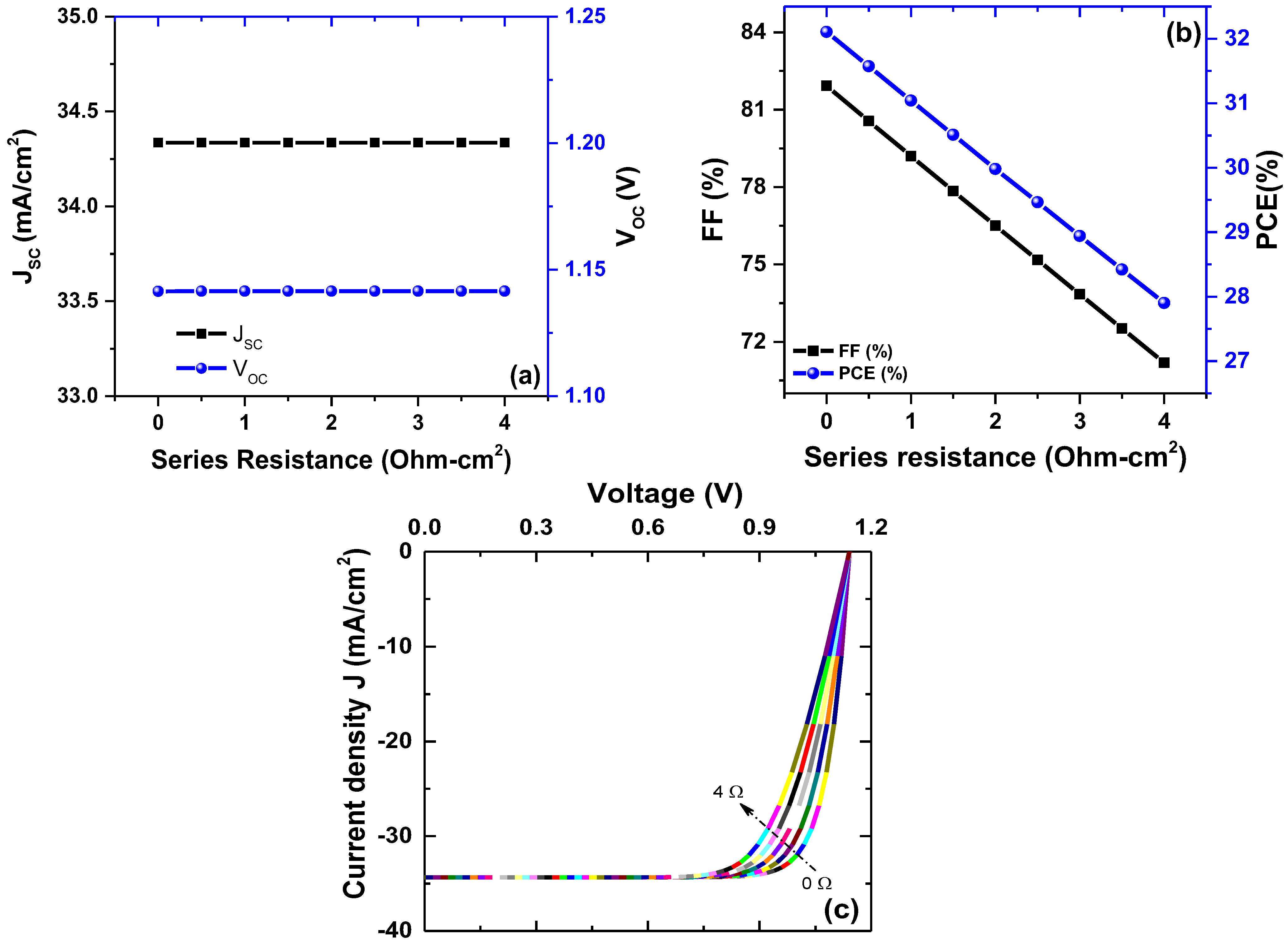
The influence of series resistance is depicted in Figure 6. As can be seen, the outputs of PSC reduce with increasing series resistances. At the resistance value of 0 Ω, its maximum efficiency possesses nearly 32.19%, and its lowest value of 27.8%, at a series resistance level of 4 Ω.
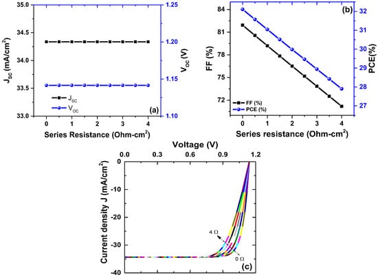
Figure 6.
Comparison of photovoltaic parameters, (a) Jsc and Voc, (b) FF and PCE and (c) J–V characteristics for MASnBr3-based PSC over different series resistance.
On the other hand, the J–V curve also shows that the impact of the resistance is more on the FF than the JSC and VOC. The highest FF for the PSC is achieved for steeper J–V, reaching a maximum value of FF 82.06%, ultimately achieving a value of PCE 32.19%. The current density of 34.09 mA/cm2 and VOC of 1.15 V is much higher than previous work by Bhattarai et al. [19].
4.6. The Collective Impact of Total Defect Density and Thickness
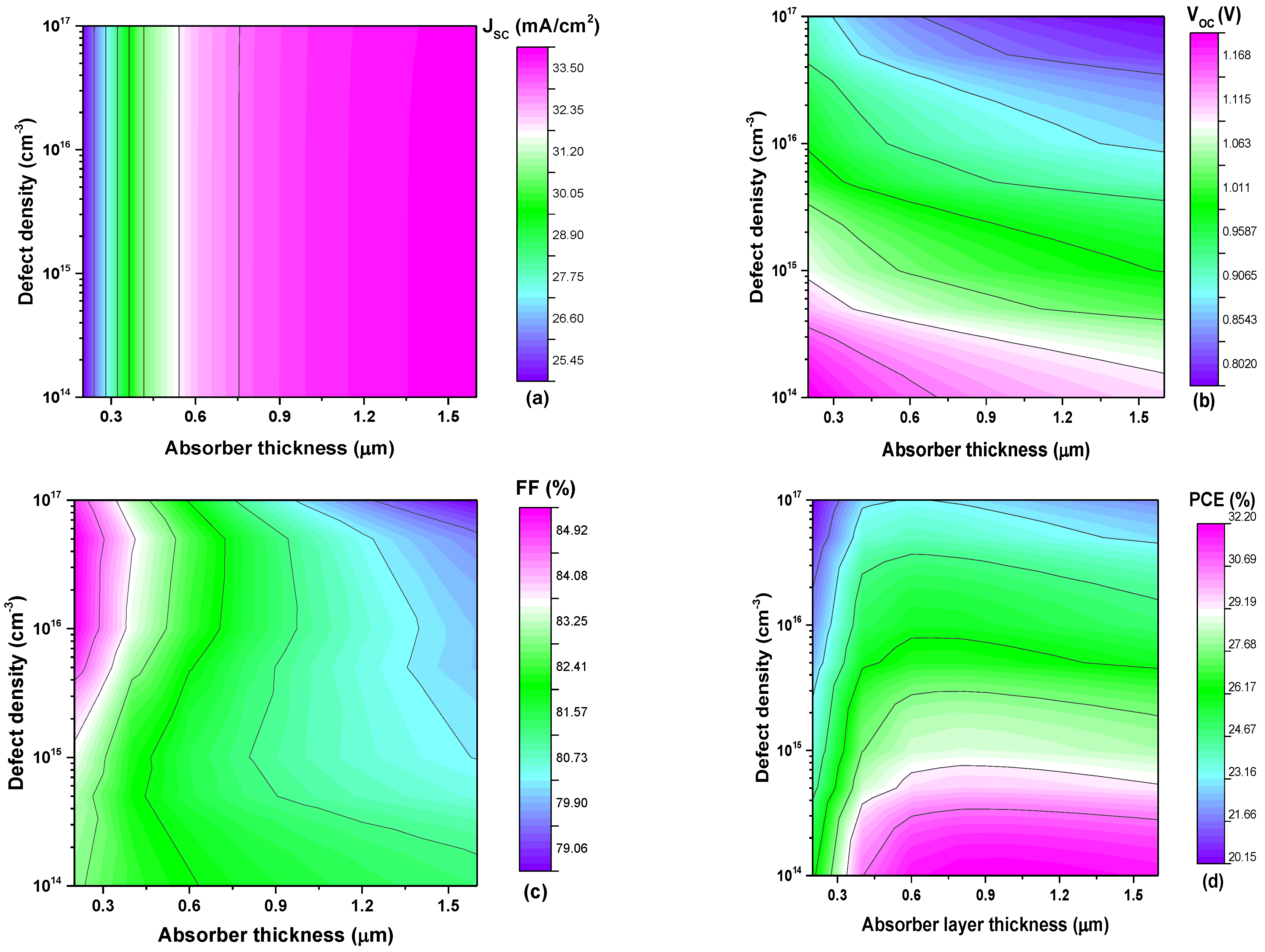
In the previous sections, the performance metrics of PSC devices have been discussed based on bulk defect density keeping the absorber layer at a fixed thickness. However, there may be defectivity at various regions of the absorber layer, which comprehend how the device performs when both defect and thickness variations are combined. Therefore, the investigation of collective variation in this direction continues to be important, which is placed in this separate subsection. Determining the perfect defectivity with suitable thickness on PSC performance as a whole is one of the prime goals in the present work. First, the defect density is increased from 1 × 1014 cm−3 to 5 × 1017 cm−3, while the thickness of the absorber layers varied from 0.2 µm to 1.6 µm, respectively.
It can be seen from Figure 7a that the JSC keeps increasing at a higher value of both thickness and defectivity. On the contrary, the VOC shows opposite characteristics with both parameters, as shown in Figure 7b. The FF parameter is highest for 0.2 µm and 5 × 1016 cm−3, as depicted in Figure 7c. Finally, the most predominant PSC parameter, i.e., PCE, reaches a maximum value for the thickness and defectivity value of 0.8 µm and 1 × 1014 cm−3 as shown in Figure 7d. The present work is much improved than the earlier work by Bhattarai et al. [19].
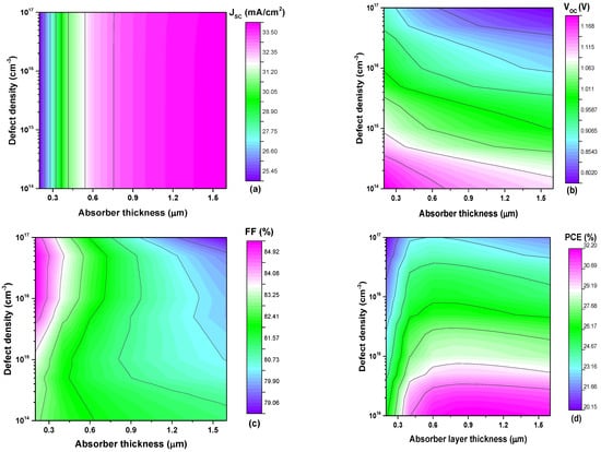
Figure 7.
Analysis of four output parameters for MASnBr3-based PSC over the combined impact of perovskite thickness and total defect density.
4.7. The Quantum Efficiency (QE) and Current vs. Voltage (JV) Analysis
It is crucial to highlight that the external quantum efficiency (EQE) of a perovskite solar cell is predominantly influenced by the light absorption properties of the absorber layer (AL). Nonetheless, it’s essential to recognize that other layers within the solar cell device can also have an impact on the overall EQE. In a representative film based-PSC structure, the AL is sandwiched between a transparent conductive oxide (TCO), often made of materials such as ITO and a cathode layer.
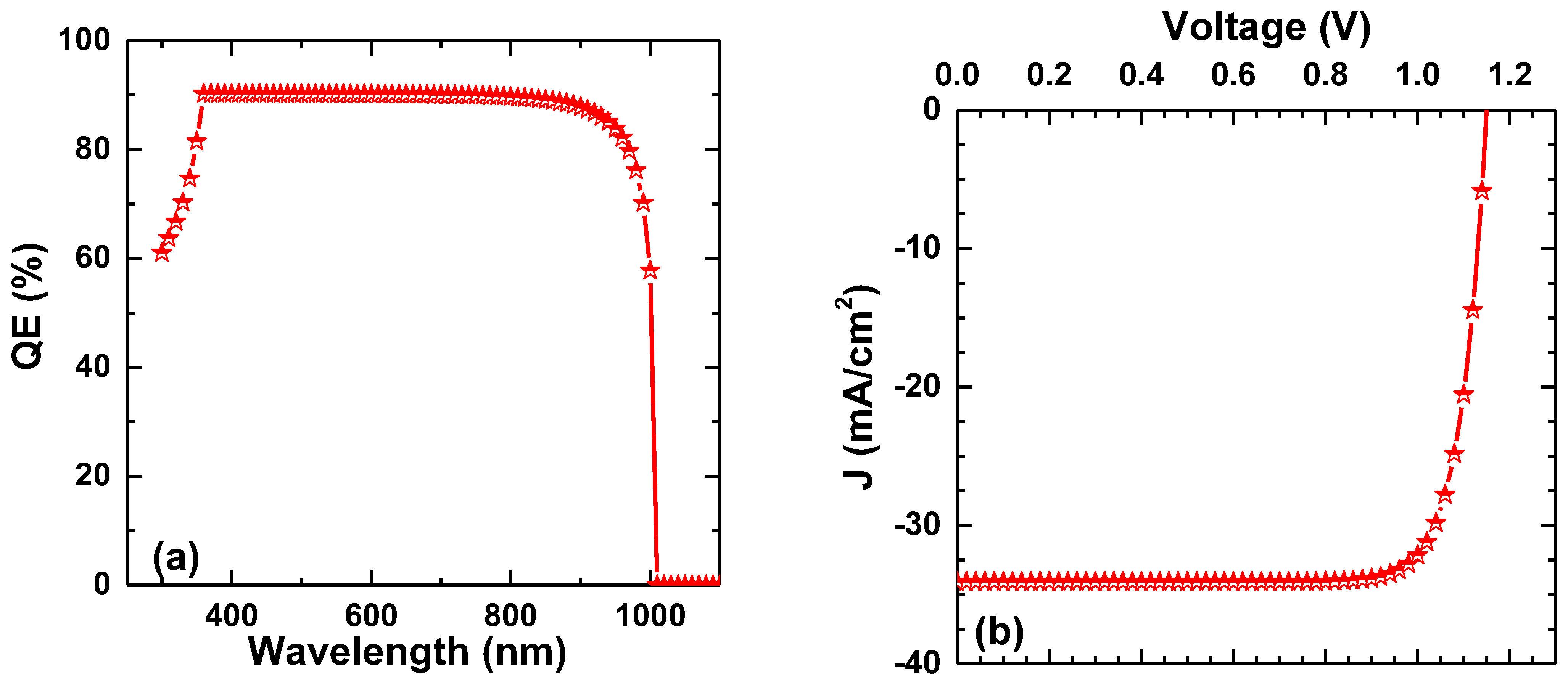
The TCO layer serves a dual purpose within the device. Firstly, it allows incident light to pass through and reach the absorber layer, thereby aiding in light absorption. Secondly, it serves as the front contact for the solar cell. If the TCO layer is excessively thick or has high resistance, it could restrict the light that reaches the AL, consequently reducing the EQE. Likewise, the back contact layer in the device affects EQE through manipulating the charge efficiency from the solar cell. If the back contact layer is not optimized for efficient charge extraction, it can lead to losses in EQE. In some solar cell architectures, additional layers are incorporated to enhance the performance of the device. As an example, PSC often include an ETL and a HTL improving charge carrier and minimize losses of recombination. Although the AL is the main contributor to the EQE in a PSC, additional layers are also influenced the overall performance. Achieving high device efficiency requires optimizing each layer and considering their interplay in order to maximize light absorption, charge extraction, and minimize recombination losses. According to Figure 8, the optimized preconditions for the MASnBr3-based PSC give a very high QE over the incident photons’ wavelength. It was found that the bandgap of the absorbing layer is inversely correlated with the solar cells’ quantum efficiency. This allows for photon absorption up to a broad range of wavelengths in the MASnBr3-based PSC. The high value of QE, i.e., 90%, is achieved for the present simulation of the MASnBr3-based PSC (Figure 8a), which is substantially more than the earlier reported result by Bhattarai et al. [24].
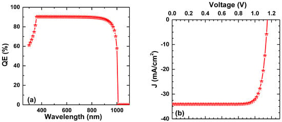
Figure 8.
(a) The QE and (b) the J–V parameter for MASnBr3-based PSC at all optimized conditions.
Figure 8b shows the current density across the voltage for the PSC device. The Sn-based PSC device produced superior JSC and VOC combinations throughout the simulation, which predicts a gain in efficiency since JSC and VOC directly affect efficiency. According to the optimal thickness conditions, defectivity (interface and total defect density), temperature, and resistivity, the highest VOC of 1.15 V is reached, as shown in Figure 8b. Additionally, the MASnBr3-based PSC device reaches the JSC of 32.44 mA/cm2. It is clear that the current density of the current simulations is greater than that of the earlier report by Du et al. [21]. Additionally, the MASnBr3-based PSC gives an FF of 82.06%, which is reliable for an ideal PSC device.
5. Conclusions
In the present work, the computational approach is conducted to optimize the optoelectronics parameters of the PSC device. The primary aim of the present work is to optimize the absorber layer thicknesses to obtain the highest efficiency and other performance metrics. The investigation offers much-optimized outputs at the thickness of 0.8 µm; simulations for various absorber layer thicknesses help us comprehend how the device performs when defect and thickness variations are combined. Determining the impact of defect density on PSC performance is the primary goal of defect density research. The efficiency is maximum at the defect density of 1 × 1014 cm−3. The optimized temperature of 300 K is also reached in the investigation. Similarly, the collective influence of the smallest series resistance value of 0 Ω offers unprecedented JSC leads to attaining the highest efficiency of 32.19% for the PSC device. Achieving such an efficiency which is near the Shockley–Queisser limit can be considered one of the main findings of the current work. Moreover, the change in the photovoltaic parameters JSC, VOC, FF and PCE induced by the change in PSC thickness, temperature, defect density and series resistance are presented in detail giving the idea about non-optimal performance of presented PSC device. The work can explicitly guide and offer better device optimization using the numerical techniques that can be fabricated in the near future.
Author Contributions
Conceptualization, S.B.; methodology, S.B.; software, S.B. and P.K.K.; validation, S.B., P.K.K. and I.H.; formal analysis, S.B. and M.Z.A.; investigation, S.B., P.K.K.; resources, S.B., A.S.A. and K.H.M.; data curation, S.B.; writing—original draft preparation, S.B., P.J. and M.Z.A.; writing—review and editing, S.B., P.J. and M.Z.A.; visualization, S.B.; supervision, P.J. and M.Z.A.; project administration, A.S.A. and K.H.M.; funding acquisition, A.S.A. and K.H.M. All authors have read and agreed to the published version of the manuscript.
Funding
The researchers would like to acknowledge the Deanship of Scientific Research, Taif University, for funding this work.
Acknowledgments
The authors would also like to express their sincere gratitude to Marc Burgelman for providing the open-source SCAPS-1D simulating software. The researchers would like to acknowledge the Deanship of Scientific Research, Taif University, for funding this work.
Conflicts of Interest
The authors declare no conflict of interest. The funders had no role in the design of the study; in the collection, analyses, or interpretation of data; in the writing of the manuscript; or in the decision to publish the results.
References
- Hima, A.; Lakhdar, N.; Benhaoua, B.; Saadoune, A.; Kemerchou, I.; Rogti, F. An optimized perovskite solar cell designs for high conversion efficiency. Superlattices Microstruct. 2019, 129, 240–246. [Google Scholar] [CrossRef]
- Bhattarai, S.; Mhamdi, A.; Hossain, I.; Raoui, Y.; Pandey, R.; Madan, J.; Bouazizi, A.; Maiti, M.; Gogoi, D.; Sharma, A. A detailed review of perovskite solar cells: Introduction, working principle, modelling, fabrication techniques, future challenges. Micro Nanostructur. 2022, 172, 207450. [Google Scholar] [CrossRef]
- Raoui, Y.; Ez-Zahraouy, H.; Kazim, S.; Ahmad, S. Energy level engineering of charge selective contact and halide perovskite by modulating band offset: Mechanistic insights. J. Energy Chem. 2021, 54, 822–829. [Google Scholar] [CrossRef]
- Snaith, H.J.; Hacke, P.J.N.E. Enabling reliability assessments of pre-commercial perovskite photovoltaics with lessons learned from industrial standards. Nat. Energy 2018, 3, 459–465. [Google Scholar] [CrossRef]
- Bhattarai, S.; Das, T.D. Optimization of carrier transport materials for the performance enhancement of the MAGeI3 based perovskite solar cell. Sol. Energy 2021, 217, 200–207. [Google Scholar] [CrossRef]
- Kojima, A.; Teshima, K.; Shirai, Y.; Miyasaka, T. Organometal Halide Perovskites as Visible-Light Sensitizers for Photovoltaic Cells. J. Am. Chem. Soc. 2009, 131, 6050–6051. [Google Scholar] [CrossRef] [PubMed]
- Muchahary, D.; Ram, L.S.; Narzary, R.; Sahu, P.P.; Bhattarai, S.; Tayal, V. Heterojunction between crystalline silicon and nanocomposite coupled ZnO·SnO2 and optimization of its photovoltaic performance. Curr. Appl. Phys. 2022, 38, 15–21. [Google Scholar] [CrossRef]
- Bhattarai, S.; Pandey, R.; Madan, J.; Ahmed, F.; Shabnam, S. Performance improvement approach of all inorganic perovskite solar cell with numerical simulation. Mater. Today Commun. 2022, 33, 104364. [Google Scholar] [CrossRef]
- Devi, C.; Mehra, R. Device simulation of lead-free MASnI3 solar cell with CuSbS2 (copper antimony sulfide). J. Mater. Sci. 2019, 54, 5615–5624. [Google Scholar] [CrossRef]
- Kumar, A.; Singh, S.; Pandey, R. Computational Modelling and Optimization of a Methylammonium-free Perovskite and Ga-free Chalcogenide Tandem Solar Cell with an Efficiency above 25 %. ChemistrySelect 2022, 7, e202200667. [Google Scholar] [CrossRef]
- Im, J.-H.; Lee, C.-R.; Lee, J.-W.; Park, S.-W.; Park, N.-G. 6.5% efficient perovskite quantum-dot-sensitized solar cell. Nanoscale 2011, 3, 4088–4093. [Google Scholar] [CrossRef] [PubMed]
- Kim, H.-S.; Lee, C.-R.; Im, J.-H.; Lee, K.-B.; Moehl, T.; Marchioro, A.; Moon, S.-J.; Humphry-Baker, R.; Yum, J.-H.; Moser, J.E.; et al. Lead Iodide Perovskite Sensitized All-Solid-State Submicron Thin Film Mesoscopic Solar Cell with Efficiency Exceeding 9%. Sci. Rep. 2012, 2, 591. [Google Scholar] [CrossRef] [PubMed]
- Liu, M.; Johnston, M.B.; Snaith, H.J. Efficient planar heterojunction perovskite solar cells by vapour deposition. Nature 2013, 501, 395–398. [Google Scholar] [CrossRef]
- Xi, J.Y.; Jia, R.; Li, W.; Wang, J.; Bai, F.Q.; Eglitis, R.I.; Zhang, H.X. How does graphene enhance the photoelectric conversion efficiency of dye sensitized solar cells? An insight from a theoretical perspective. J. Mater. Chem. A 2019, 7, 2730–2740. [Google Scholar] [CrossRef]
- Bhattarai, S.; Das, T.D. Optimization of the perovskite solar cell design to achieve a highly improved efficiency. Opt. Mater. 2021, 111, 110661. [Google Scholar] [CrossRef]
- Bhattarai, S.; Sharma, A.; Muchahary, D.; Gogoi, D.; Das, T.D. Numerical simulation study for efficiency enhancement of doubly graded perovskite solar cell. Opt. Mater. 2021, 118, 111285. [Google Scholar] [CrossRef]
- Ahmed, M.I.; Habib, A.; Javaid, S.S. Perovskite Solar Cells: Potentials, Challenges, and Opportunities. Int. J. Photoenergy 2015, 205, 592308. [Google Scholar] [CrossRef]
- Lakhdar, N.; Hima, A.J.O.M. Electron transport material effect on performance of perovskite solar cells based on CH3NH3GeI3. Opt. Mater. 2020, 99, 109517. [Google Scholar]
- Bhattarai, S.; Pandey, R.; Madan, J.; Mhamdi, A.; Bouazizi, A.; Muchahary, D.; Gogoi, D.; Sharma, A.; Das, T.D. Investigation of Carrier Transport Materials for Performance Assessment of Lead-Free Perovskite Solar Cells. IEEE Trans. Electron Devices 2022, 69, 3217–3224. [Google Scholar] [CrossRef]
- Huang, P.-H.; Wang, Y.-H.; Ke, J.-C.; Huang, C.-J. The Effect of Solvents on the Performance of CH3NH3PbI3 Perovskite Solar Cells. Energies 2017, 10, 599. [Google Scholar] [CrossRef]
- Du, H.-J.; Wang, W.-C.; Zhu, J.-Z. Device simulation of lead-free CH3NH3SnI3 perovskite solar cells with high efficiency. Chin. Phys. B 2016, 25, 108802. [Google Scholar] [CrossRef]
- Noel, N.K.; Stranks, S.D.; Abate, A.; Wehrenfennig, C.; Guarnera, S.; Haghighirad, A.-A.; Sadhanala, A.; Eperon, G.E.; Pathak, S.K.; Johnston, M.B.; et al. Lead-free organic–inorganic tin halide perovskites for photovoltaic applications. Energy Environ. Sci. 2014, 7, 3061–3068. [Google Scholar] [CrossRef]
- Umari, P.; Mosconi, E.; Angelis, F.D. Relativistic GW calculations on CH3NH3PbI3 and CH3NH3SnI3 Perovskites for Solar Cell Applications. Sci. Rep. 2014, 4, 4467. [Google Scholar] [CrossRef]
- Bhattarai, S.; Pandey, R.; Madan, J.; Muchahary, D.; Gogoi, D. A novel graded approach for improving the efficiency of Lead-Free perovskite solar cells. Sol. Energy 2022, 244, 255–263. [Google Scholar] [CrossRef]
- Mottakin, M.; Sobayel, K.; Sarkar, D.; Alkhammash, H.; Alharthi, S.; Techato, K.; Shahiduzzaman, M.; Amin, N.; Sopian, K.; Akhtaruzzaman, M. Design and Modelling of Eco-Friendly CH3NH3SnI3-Based Perovskite Solar Cells with Suitable Transport Layers. Energies 2021, 14, 7200. [Google Scholar] [CrossRef]
- Jeon, I.; Kim, K.; Jokar, E.; Park, M.; Lee, H.-W.; Diau, E.W. Environmentally Compatible Lead-Free Perovskite Solar Cells and Their Potential as Light Harvesters in Energy Storage Systems. Nanomaterials 2021, 11, 2066. [Google Scholar] [CrossRef]
- Burgelman, M.; Verschraegen, J.; Degrave, S.; Nollet, P. Modeling thin-film PV devices. Prog. Photovolt. 2004, 12, 143–153. [Google Scholar] [CrossRef]
- Burgelman, M.; Marlein, J. Analysis of graded band gap solar cells with SCAPS. In Proceedings of the 23rd European Photovoltaic Conference, Valencia, Spain, 1–5 September 2008. [Google Scholar]
- Bhattarai, S.; Sharma, A.; Das, T.D. Factor affecting the performance of perovskite solar cell for distinct MAPI layer thickness. AIP Conf. Proc. 2020, 2269, 030071. [Google Scholar]
- Elumalai, N.K.; Mahmud, M.A.; Wang, D.; Uddin, A. Perovskite Solar Cells: Progress and Advancements. Energies 2016, 9, 861. [Google Scholar] [CrossRef]
- Karthick, S.; Velumani, S.; Bouclé, J. Experimental and SCAPS simulated formamidinium perovskite solar cells: A comparison of device performance. Sol. Energy 2020, 205, 349–357. [Google Scholar] [CrossRef]
- Rai, S.; Pandey, B.K.; Dwivedi, D.K. Modeling of highly efficient and low cost CH3NH3Pb(I1-xClx)3 based perovskite solar cell by numerical simulation. Opt. Mater. 2020, 100, 109631. [Google Scholar] [CrossRef]
- Al-Mousoi, A.K.; Mohammed, M.K.A.; Pandey, R.; Madan, J.; Dastan, D.; Ravi, G.; Sakthivel, P.; Anandha babu, G. Simulation and analysis of lead-free perovskite solar cells incorporating cerium oxide as electron transporting layer. RSC Adv. 2022, 12, 32365–32373. [Google Scholar] [CrossRef] [PubMed]
- Samiul Islam, M.; Sobayel, K.; Al-Kahtani, A.; Islam, M.A.; Muhammad, G.; Amin, N.; Shahiduzzaman, M.; Akhtaruzzaman, M. Defect Study and Modelling of SnX3-Based Perovskite Solar Cells with SCAPS-1D. Nanomaterials 2021, 11, 1218. [Google Scholar] [CrossRef] [PubMed]
- Liu, D.; Kelly, T.L. Perovskite solar cells with a planar heterojunction structure prepared using room-temperature solution processing techniques. Nat. Photonics 2014, 8, 133–138. [Google Scholar] [CrossRef]
- Ebner, M.; Marone, F.; Stampanoni, M.; Wood, V.J.S. Visualization and quantification of electrochemical and mechanical degradation in Li ion batteries. Science 2013, 342, 716–720. [Google Scholar] [CrossRef]
- Fossum, J.G. Computer-aided numerical analysis of silicon solar cells. Solid State Electron. 1976, 19, 269–277. [Google Scholar] [CrossRef]
- Bhattarai, S.; Sharma, A.; Muchahary, D.; Gogoi, M.; Das, T.D. Carrier transport layer free perovskite solar cell for enhancing the efficiency: A simulation study. Optik 2021, 243, 167492. [Google Scholar] [CrossRef]
- Singh, A.K.; Srivastava, S.; Mahapatra, A.; Baral, J.K.; Pradhan, B. Performance optimization of lead free-MASnI3 based solar cell with 27% efficiency by numerical simulation. Opt. Mater. 2021, 117, 111193. [Google Scholar] [CrossRef]
Disclaimer/Publisher’s Note: The statements, opinions and data contained in all publications are solely those of the individual author(s) and contributor(s) and not of MDPI and/or the editor(s). MDPI and/or the editor(s) disclaim responsibility for any injury to people or property resulting from any ideas, methods, instructions or products referred to in the content. |
© 2023 by the authors. Licensee MDPI, Basel, Switzerland. This article is an open access article distributed under the terms and conditions of the Creative Commons Attribution (CC BY) license (https://creativecommons.org/licenses/by/4.0/).

