Review

Research Progress of Micro-LED Display Technology

1
DGUT-CNAM Institute, Dongguan University of Technology, Dongguan 523808, China
2
School of Information and Optoelectronic Science and Engineering, South China Normal University, Guangzhou 510631, China
3
Institute of Semiconductors, Guangdong Academy of Sciences, Guangzhou 510650, China
4
Centre for Translational Atomaterials, School of Science, Swinburne University of Technology, Hawthorn, VIC 3122, Australia
5
School of Materials Science and Engineering, South China University of Technology, Guangzhou 510640, China
*
Author to whom correspondence should be addressed.
These authors contributed equally to this work.
Crystals 2023, 13(7), 1001; https://doi.org/10.3390/cryst13071001
Submission received: 15 May 2023 / Revised: 30 May 2023 / Accepted: 20 June 2023 / Published: 23 June 2023
(This article belongs to the Special Issue Semiconductor Nanocrystals)

Abstract

:
Micro-LED display technology is considered to be the next generation of display technology, which has the characteristics of high miniaturization, thin film and integration, as well as the advantages of high brightness, high contrast, fast response speed and long service life. However, in the development of Micro-LED display technology, there are still some technical and cost problems to be solved. This paper focuses on the key technologies involved in Micro-LED display technology, such as chip technology, mass transfer, full-color display, bonding and driving technology, the research history and frontier progress of these technologies are reviewed in detail. For chip epitaxy technology, the wavelength uniformity, current density and defect control are emphasized; for chip process, the two main chip structures and the challenges brought by miniaturization are discussed emphatically; for chip integration, full-color display, backplane bonding and driving, several mainstream technical schemes are summarized in turn. Finally, the chip detection and repair technologies and commercial application are introduced.

1. Introduction

In the past few decades, display technologies in the form of TVs, tablet computers, smart devices, and billboards have been widely used, covering all aspects from social production activities to people’s daily life [1]. The cathode ray tube (CRT) display technology was first used for video display, which once occupied the dominant position in the display market from the 1950s to the beginning of this century. Since 2000, liquid crystal display (LCD) and organic light emitting diode (OLED) display technology has been widely used, and gradually dominate the display market. In recent years, with the rise of miniature displays such as virtual reality (VR) and augmented reality (AR), as well as giant displays such as display walls, LCD and OLED display technologies can hardly meet the needs of emerging display applications, thus stimulating the development of new display technologies with higher performance [2].
LCD is a non-self-emissive display technology, it needs to rely on the backlight to achieve the display effect. The backlight of the LCD panel passes through the polarizer and then enters the color filter to convert white light into RGB three-color light, thus realizing full-color display. Based on the characteristics of this display technology, its display angle is not high, its response speed is slow and it is not easy to bend [3]. OLED is a self-emissive display technology, and its emissive materials are usually small molecules or high polymers, which are formed by vacuum evaporation, spin coating and inkjet printing. Compared with LCD, it has fast response speed, high viewing angle and good flexibility, and does not need a backlight unit. However, due to the limitation of its material itself, there are still problems such as low color purity, low environmental stability and low temperature tolerance range, which limits its application in display [4]. Therefore, Micro-LED display technology has attracted extensive attention of researchers.
With the development of Micro-LED display technology, there are different views on the definition of Micro-LED and Mini-LED in the academic and industrial fields [5]. There is a view that LEDs with a size below 100 μm are called “Micro-LEDs”, and LEDs with a size of 100~200 μm are called “Mini-LEDs” [6]. There are also views that the Micro-LED chip size is smaller than 50 μm [7] or light emitting area is less than 2000 μm2 [8]. Mini-LED is generally used as the backlight of LCD, while Micro-LED, as a display technology, is considered to have the potential to replace or partially replace the LCD and OLED display markets. Compared with other displays, the outstanding performance parameters of Micro-LED are shown in Table 1.
As a new display technology, Micro-LED display technology is mainly based on the third-generation semiconductor material gallium nitride (GaN), and its unique advantages of low power consumption, high brightness, fast response and high reliability have attracted extensive attention from industry and academia [9,10,11,12,13]. In addition to display applications, since 2000, Micro-LED has been studied to improve the luminous efficiency of high-intensity lighting because of its relatively high light extraction efficiency, better current expansion and lower self-heating effect [14,15,16].
In 2000, Jiang et al., of Kansas State University prepared Micro-LED [17], laying a theoretical and experimental foundation for the development of Micro-LED, and in 2001, a 10 × 10 blue Micro-LED array with a chip size of 12 μm was prepared [18]. In 2004, Dawson et al., University of Clyde, UK prepared a 64 × 64 ultraviolet (UV) Micro-LED array with a chip size of 20 μm [19], and in 2007, a 16 × 16 blue Micro-LED array with a chip size of 72 μm was fabricated by flip-chip structure [20]. In 2008, Poher et al., of Imperial College London prepared a 64 × 64 blue, green and UV Micro-LED array with a chip size of 20 μm [21]. In 2011, Lin et al., of Texas Tech University prepared a 160 × 120 green Micro-LED array with a chip size of 12 μm using indium bump flip-chip bonding technology [22]. In 2013, Liu et al., of Hong Kong University of Science and Technology prepared UV and red, green and blue Micro-LED arrays with a chip size of 50 μm and pixels per inch (PPI) is 360 [23], and in 2014, they prepared blue Micro-LED arrays with a chip size of 15 μm and a PPI of 1700 [24]. In 2015, Kuo et al., of National Chiao Tung University prepared a 128 × 128 red, green and blue Micro-LED array with a chip size of 35 μm on the UV Micro-LED array by quantum dots (QDs) spraying technology [25], and in 2017, the photoresist mold was used to improve the spraying accuracy of QDs and reduce the optical crosstalk of pixels [26]. In 2020, Wang et al., of the University of Sheffield in the UK prepared a green Micro-LED array with a chip size of 3.6 μm on a sapphire substrate using a SiO2 mask, and the process did not involve mesa etching process, thus avoiding the damage caused by etching [27]. In 2023, researchers from Massachusetts Institute of Technology and other universities in the United States and South Korea realized the vertical full-color Micro-LED array with the highest (5100 PPI) and the smallest chip size (4 μm) reported so far in PPI through two-dimensional material layer transfer technology [28].
It has been more than 20 years since the concept of Micro-LED was put forward and developed into a popular technology. Although there have been corresponding solutions for the more difficult processes in Micro-LED display technology, such as epitaxial technology of materials, chip preparation, full color display, etc., there is still a way to go before commercialization is achieved. The following will introduce the research status of chip technology, mass transfer, monolithic integration, full-color display, bonding and driving, detection and repair technology in Micro-LED display technology in detail, and prospect its commercial application prospects.

2. Micro-LED Chip Technology

2.1. Epitaxy Technology

The crystal quality of the epitaxial wafer used to prepare Micro-LED chips will directly affect the display effect. Therefore, it is necessary to ensure high uniformity of the light emission wavelength and current density of the epitaxial wafer and low defect density [29]. Due to factors such as stress relaxation, current expansion and multibody effect [30,31,32], the internal quantum efficiency (IQE) of Micro-LED chips is higher than that of large LED chips at high current density. However, Micro-LED chips are used as displays at low current density, and the increase in the ratio of non-radiative compounding caused by surface defects can lead to a decrease in radiative compounding efficiency and thus a decrease in IQE. IQE can be improved by using sidewall passivation, thermal annealing, and wet chemical treatment [33,34,35,36], as well as by using non-damaging etching methods instead of inductively coupled plasma (ICP) etching, or novel preparation methods to avoid etching of GaN [27,37].
Dislocation density affects the performance of Micro-LED chips, making the luminescence characteristics different from chip to chip, so the defect density of epitaxial wafers needs to be reduced. Using GaN as a homoepitaxial substrate can improve device quality, and hydride vapor phase epitaxy (HVPE) can be used to grow GaN epitaxial layers, but the size of GaN layers grown by HVPE technology is limited, and it is difficult to control the thickness of GaN films, high technical difficulty [38]. At present, heterogeneous epitaxial substrates (such as silicon (Si), sapphire (α-Al2O3), silicon carbide (SiC), etc.) are mainly used to grow GaN layers. The dislocation density of heteroepitaxy can be reduced by adding buffer layers (such as AlGaN/AlN buffer layer, AlN/GaN superlattice buffer layer, AlxGa1-xN buffer layer, etc.), lateral epitaxy (ELO) and patterned substrates [39,40,41,42].
In order to meet the demand of large-size monolithic display, the substrate for growing GaN should be developed to a large diameter, but it brings difficulties in the uniformity of light emission wavelength. The emission wavelength of InGaN/GaN LED is related to the indium composition, which is related to the temperature and gas flow during epitaxy. In component in InGaN will cause wavelength deviation of 1.8 nm and 2.5 nm for blue and green LEDs respectively at a temperature difference of 1 °C [43]. The lattice mismatch and thermal mismatch between GaN and heterogeneous substrate will cause bending during epitaxial wafer growth, resulting in temperature inhomogeneity, which further makes the spatial inhomogeneous distribution of indium in the InGaN/GaN multiple quantum well (MQW) on the whole epitaxial wafer. In order to improve the uniformity of emission wavelength of epitaxial wafer, measures such as increasing the thickness of substrate, improving graphite disk, laser treating substrate and adding insertion layer can be taken [44,45,46,47]. The gas flow during epitaxy is mainly related to metal organic chemical vapor deposition (MOCVD) equipment. MOCVD technology is the core technology for preparing epitaxial wafers of optoelectronic materials such as GaAs, InP, and GaN [48]. The high-brightness blue LED prepared by Shuji Nakamura uses MOCVD technology with dual airflows. MOCVD technology has the advantages of high purity of source material (up to 99.9999%), accurate control of gas pressure and flow rate, and can be used for epitaxial growth of large-size substrates or multiple substrates. The MOCVD equipment with planetary reaction chamber structure of Aixtron Company in Germany uses gas foil to rotate each wafer tray, which can realize the uniform growth of a single wafer, and improve the uniformity between wafers through secondary rotation. By adding Cl2 in-situ cleaning process and cassette to cassette process between each operation, the defect density with the size greater than 1 μm is as low as about 0.1 defect/cm2, and the wavelength standard deviation of an 8-inch silicon-based blue LED epitaxial wafer is about 1 nm [49]. Veeco Company of the United States uses TurboDisc reaction chamber, and adopts vertical rotating disc technology to realize high capacity, low defect density and high uniformity of 14 × 6-inch sapphire-based epitaxial wafer. On 8-inch silicon-based blue LED epitaxial wafer, the uniformity of emission wavelength is 1–2 nm [11].

2.2. Chip Structure

Micro-LED chip structure is mainly divided into vertical structure and flip-chip structure, and the forward structure widely used in lighting is generally not used in Micro-LED display. Vertical chips are better for near-eye displays because the effective active area of vertical chips is larger. Flip-chip is commonly used for display applications with less than 1000 PPI, while vertical chip is commonly used for display applications with more than 1000 PPI. Vertical chip and flip-chip have their own advantages and disadvantages: with the miniaturization of chip size, flip-chip needs more process steps, and for the two chips with the same size, the p and n electrode pads in flip-chip are smaller than vertical chip, and the required equipment is higher. The vertical chip structure adopts the method of wafer direct bonding, and its current path is helpful for current diffusion [50]; However, flip-chip InGaN Micro-LED can avoid the complicated laser lift-off (LLO) process, and the connection of n and p electrode pads can be completed in one step in the bonding process, so flip-chip bonding is easier [7].
Figure 1 is a schematic diagram of the AlInGaP red vertical Micro-LED device structure, and its process flow is as follows: (1) AlInGaP epitaxial wafers were grown on n-type lattice-matched GaAs substrates by MOCVD, and then indium tin oxide (ITO) layers for ohmic contact and current diffusion were deposited on AlInGaP epitaxial wafers by electron gun evaporation machine, (2) polished sapphire was bonded with ITO by glue, (3) GaAs substrates were removed by wet chemical etching, (4) AuGe/Au was deposited, (5) The mesa structure is formed by dry etching (etching to the ITO layer), (6) the ITO is etched (etching to the glue adhesive layer), (7) the metal platform with the same height as the Micro-LED chip is deposited, (8) the array is planarized with polymer, (9) the Ti/Al/Ti/Au (50 nm/2.3 µm/50 nm/60 nm) metal layer is deposited [9].
The fabrication process of InGaN Micro-LED flip-chip is similar to that of traditional LED flip-chip, but the size of the Micro-LED chip is much smaller. Figure 2 is a schematic cross-sectional view of a flip-chip InGaN Micro-LED bonded to a complementary metal oxide semiconductor (CMOS) driver backplane [51]. The driving backplane can be a printed circuit board (PCB), a CMOS backplane or a thin film transistor (TFT) backplane [52]. The general process of flip-chip includes: (1) depositing ITO, Ni or Ni/Au layer as p electrode, (2) depositing Al or Ag reflector by electron beam, and (3) defining and forming pixels by inductively coupled plasma-reactive etching (ICP-RIE). (4) depositing Ti/Al as a common cathode, (5) depositing SiO2 or SiN passivation layer by plasma enhanced chemical vapor deposition (PECVD) or atomic layer deposition (ALD), (6) depositing indium or gold bumps on the metal electrode, and (7) bonding the Micro-LED array to the CMOS driver. The way of light emission is bottom emission, that is, the light is emitted from the side of the sapphire substrate [7].

2.3. Miniature Challenge

Due to the miniaturization of light-emitting chips, their luminous efficiency will drop rapidly. The emission efficiency of both blue and green chips will decrease, but compared with the significant decrease of the emission efficiency of red chips, the decrease of efficiency is acceptable in product application. It is difficult to manufacture high-efficiency InGaN-based red Micro-LED chips because with the increase of indium content, the radiation recombination rate is relatively low, and the crystal quality will deteriorate [53]. Due to the low luminous efficiency of red LED chips, the academician Jiang’s research team used efficient InGaN-based orange-red LED chips, which greatly improved the luminous efficiency of red LED chips [54].
In addition, ICP etching will cause sidewall defects, which will greatly reduce the light emitting area of Micro-LED chips. As shown in Figure 3, the defect of about 2 μm in the traditional LED chip with the size of 250 μm will not affect the chip performance too much, while the error of 2 μm in the Micro-LED chip with the size of only 5 μm will reduce the external quantum efficiency from about 35% to 10% or even 2%, and the remaining available luminous area of the chip is only 4% of the chip size.

3. Mass Transfer and Monolithic Integration Technology

According to the different sizes of Micro-LED display devices, there are two main ways of miniaturization and integration, one is for the mass transfer of large and medium-sized displays, and the other is for the monolithic integration of small-sized displays [55]. The mass transfer technology is to accurately pick up and place red, green and blue Micro-LED chips from the original substrate to the target backplane, and then connect the light-emitting chips with the driving circuit. Mass transfer provides a feasible scheme for realizing colorization. Monolithic integration technology avoids the complicated pick-and-place process. The method is to make the Micro-LED epitaxial wafer into an N×N Micro-LED chip array, and then bond the chip array with the driving backplane. This method cannot directly realize colorization, so it is necessary to combine color conversion materials to achieve the color display effect, as shown in Figure 4, which is a schematic diagram of two methods including massive transfer and monolithic integration. The two technologies will be introduced in detail below.

3.1. Mass Transfer

The traditional mechanical transfer equipment can’t meet the requirements for the transfer of Micro-LED chips in millions of mass production, because this process requires extremely high transfer rate, alignment accuracy, bonding strength and reliability. For a 4K ultra high definition (UHD) color TV, about 25 million Micro-LED chips need to be transferred, and it takes more than two months according to the traditional transfer equipment and technology, which obviously cannot meet the requirements of mass production [1]. Therefore, it is necessary to rely on mass transfer technology to meet mass production requirements. Mass transfer technology includes polydimethylsiloxane (PDMS) stamp transfer, laser transfer, fluid transfer, electrostatic transfer and electromagnetic transfer, etc.

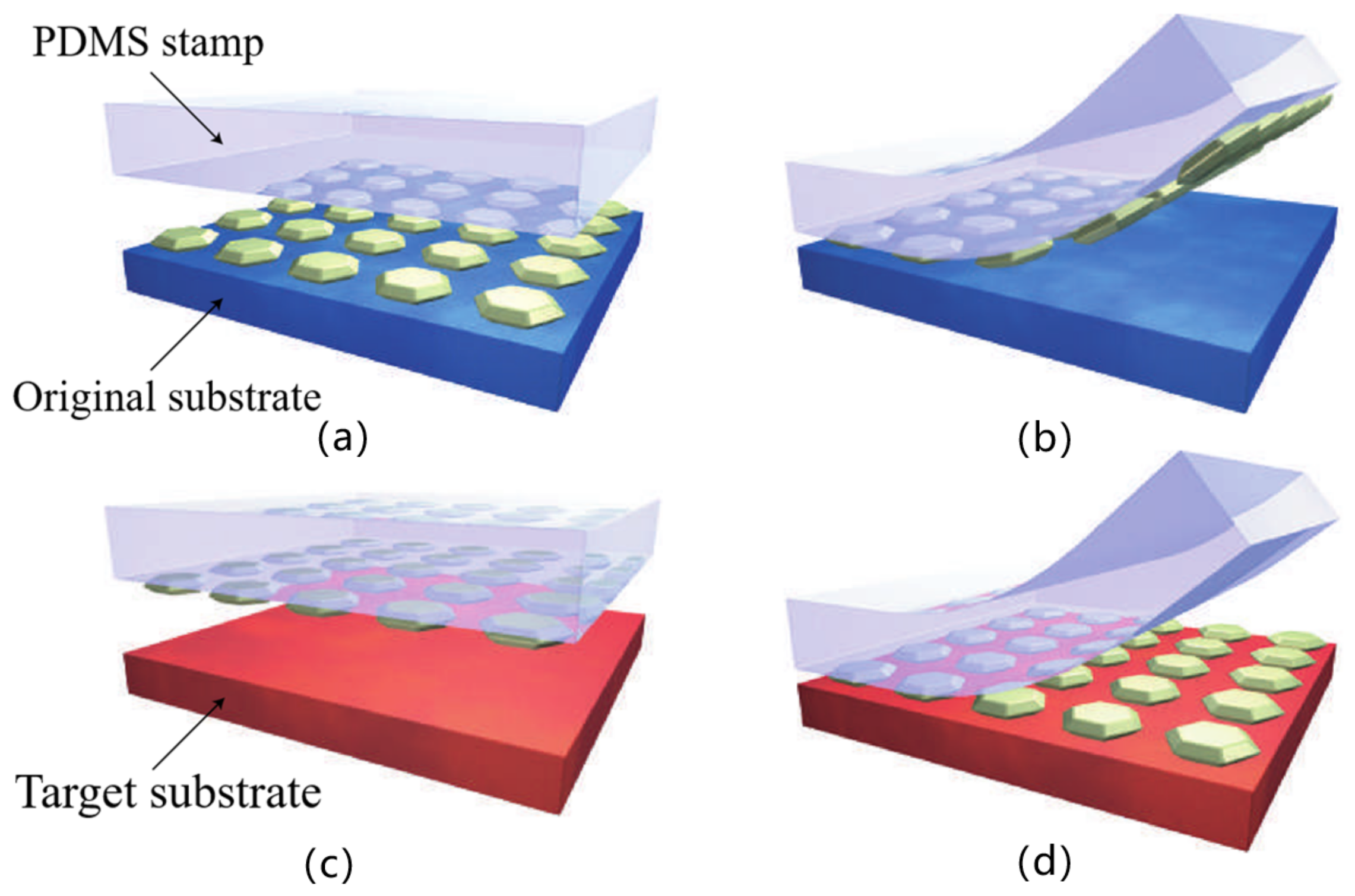
3.1.1. PDMS Stamp Transfer

As shown in Figure 5, the US X-Celeprint company uses PDMS stamp transfer technology to pick up and place Micro-LED chips [56]. Micro-LED chip is fabricated on a wafer with a sacrificial layer (such as graphene, boron nitride (BN), MoS2 and other two-dimensional materials [50,57,58,59]), and then a soft elastic stamp is used to contact the light-emitting chip. At a sufficiently high peeling rate, the chip and the stamp are bonded together due to van der Waals force. Then the chip is separated from the stamp by a sufficiently low peeling rate and adhered to the target substrate. The van der Waals force mainly utilizes the adhesion relationship between the PDMS stamp and other materials, and the adhesion relationship is related to the peeling rate. Therefore, the transfer can be achieved by changing the peeling rate [60].
PDMS stamp is non-toxic, stable, highly viscoelastic, transparent and can be optically aligned. PDMS stamp is made of flexible elastomer with rigid glass substrate, which is rigid in the horizontal x-y direction and can minimize the deformation in the printing device array; It is flexible in the vertical Z direction, so that it can make large-area contact even on an incomplete flat substrate [61]. PDMS stamp can transfer 82,863 chips of 75 μm × 90 μm with 99.99% yield in a single printing operation and can transfer chips of 3 μm in size [7]. In addition, PDMS stamp can be precisely customized according to the size of the target substrate, and it can still be used effectively after transferring tens of thousands of times [62]. For Micro-LED chips with specific arrangement and size, special PDMS stamps with structured microcolumns can also be made for selective batch transfer [63].
In addition to the above-mentioned contact transfer technology, there are also non-contact transfer technologies. Non-contact transfer technology can be independent of the properties and manufacturing process of the target substrate surface, and is not affected by the peeling rate of PDMS stamp, the cleanliness and smoothness of the material surface, but only related to the difference of thermo-mechanical response between microstructure devices and PDMS stamp. Some researchers have developed non-contact laser-driven transfer printing technology [64,65].
The process flow of non-contact laser micro-transfer printing used by Rogers et al., of the University of Illinois, USA, is shown in Figure 6 [64]. Since the PDMS stamp is transparent in the near-infrared range, the laser can transmit energy to the microstructure device through the stamp, and the microstructure device temperature rises to transfer heat to the stamp, and the temperature rise of both leads to thermal expansion, which further generates interfacial stress, and when the delamination energy release rate at the interface is greater than the adhesion force at the interface, the microstructure device will separate from the PDMS stamp.
PDMS stamps can not only adopt a flat structure, but also use a curved surface structure for transfer printing. This curved surface transfer technology is called roller transfer technology. Korea Institute of Machinery and Materials (KIMM) proposed the roller transfer technology, in which the chip was transferred to the roller with PDMS stamp, and then the Micro-LED was accurately transferred to the corresponding position of the Si-TFT on the target substrate through the microscope on the roller transfer machine. This process can reach the transmission rate of 10,000 chips per second, and also has the advantages of low cost, high yield and high efficiency [66].

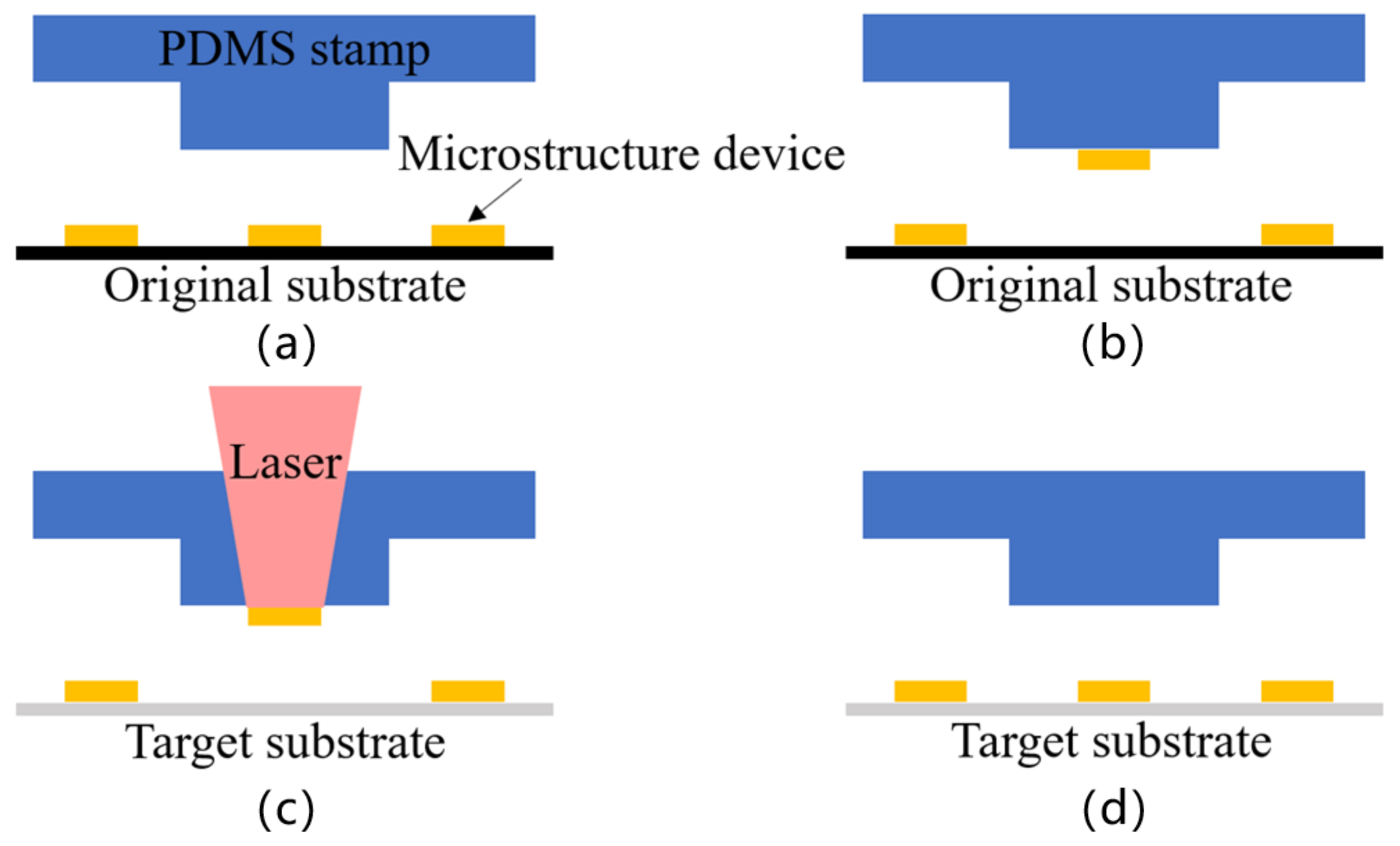
3.1.2. Laser Transfer

Laser transfer avoids the step of grasping the Micro-LED chip with PDMS stamp, and it uses the characteristics of different band gaps between different materials to complete the transfer [67,68,69,70]. The following introduces a laser selective release transfer technology demonstrated by Japan’s Sony Corporation [71]. Firstly, a semiconductor layer, a p-type electrode layer and a sacrificial layer are prepared on the original substrate, and resin or metal can be used as the sacrificial layer. The Micro-LED chips are then bonded to a temporary transfer substrate, both of which are transparent to the laser used. The laser is irradiated on the interface between the original substrate and the Micro-LED chip, and the semiconductor layer at the interface is decomposed due to high temperature, thereby separating the original substrate from the Micro-LED chip. Afterwards, the n-type electrode is prepared for the Micro-LED chip on the temporary transfer substrate, and the electrode and a separate Micro-LED chip are formed through photolithography and etching steps. Subsequently, the target substrate and the n-type electrode are bonded, and then the temporary transfer substrate is selectively laser-lifted, so that the chip is selectively transferred from the temporary transfer substrate to the target substrate.
Alternatively, the mass transfer process can be accomplished using laser-induced forward transfer, a transfer technique that can transfer about 1000 chips in one laser shot [72]. However, this technology may cause depressions and cracks on the surface of the chip, and the addition of an electroplated nickel support layer can reduce the stress generated during peeling and improve the peeling yield. As for the adhesive material, we can refer to the polyimide material used in OLED display, which will decompose when irradiated by laser, so it can also be used as a temporary transfer substrate for transfer [54]. The patterned LLO transfer technology used by Optovate in the UK can transfer blue Micro-LED chips from a sapphire wafer to a target substrate. The US Uniqarta company uses massively parallel laser enabled transfer (MPLET) technology to achieve a transfer rate of more than 100 million times per hour [73]. The US QMAT company uses the beam addressed release (BAR) mass transfer method, which transfers more than 100 to 250 million chips per hour. For a 65-inch UHD TV screen, the assembly time is about 10 min [74]. Laser transfer technology can transfer a large number of Micro-LED chips, but in order to ensure the goodness of chip transfer, the requirements for laser power, spot size, pulse width and GaN thickness are relatively high. In addition, compared with the laser spot with uniform energy density, the laser with Gaussian distribution can better avoid damage, because the laser with Gaussian distribution can make the temperature distribution at the edge of the laser irradiation area smaller, thus generating less nitrogen pressure and thermal stress. Besides using Gaussian laser to improve the transfer quality, we can also insert sacrificial layer or barrier layer between GaN and sapphire, such as inserting carbon nanotubes into the interface between GaN and sapphire, which can effectively increase the temperature of GaN, thus lowering the required energy threshold, and introduce femtosecond laser to avoid damage [75].

3.1.3. Self-Assembly Transfer

Fluid-based assembly is a cost-effective technology and can be used to transfer large-pitch Micro-LED. This technology can easily manage the microstructure on a large-area substrate with high yield. In addition, compared with other available transmission methods, the parasitic effect of interconnection is low [76]. Although this technology has some advantages, it is not mature enough such as low melting point alloy bonding, and it still needs to be further developed for commercial use [4].
The fluid assembly technology of US eLux Company uses carrier liquid to transfer Micro-LED chip to TFT backplane [77]. As shown in Figure 7, the TFT backplane has a hole structure, and each hole structure has two electrodes with solder on the electrodes. The liquid suspension loaded with Micro-LED chips flows through the TFT backplane, and then is captured by the holes and bonded with the solder at the bottom of the holes. Suspension used in fluid assembly can be acetone, isopropanol, distilled water, etc. The protrusions on the Micro-LED chip help to align and adjust the orientation of the device. If the Micro-LED chip is not oriented correctly, the flow of liquid will flip the chip to the correct orientation, or it may be squeezed out and flow into the next hole. After the positioning of the Micro-LED chip is completed, the integrated device will be annealed to melt the solder on the electrode to realize the connection between the chip and the electrode at the bottom of the hole. In addition, the use of photoluminescence (PL) and defect detection during chip processing can only collect good chips in the fluid. This method is a self-alignment process, and the pitch of Micro-LEDs is not limited by the accuracy of the transfer equipment.
For magnetic self-assembly, a thin strip of ferromagnetic materials (such as nickel, iron, etc.) is deposited in the center of the surface of the Micro-LED chip as a p-type contact, and the left and right adjacent metal pads are used as an n-type contact [78]. In the process of magnetic assembly, the Micro-LED chip is placed on the vibrating magnetic substrate. Magnets with opposite polarities are arranged next to each other on the workbench. The center between adjacent magnets becomes the node of maximum magnetic field strength. When magnetic Micro-LED chips are placed on a vibrating magnetic table, they can be randomly dispersed by vibration. With the help of the magnetic field, the chips are arranged parallel to each other at the node with the maximum magnetic field strength to realize the self-assembly process [75].For electrical self-assembly, O’Riordan et al., reported an assembly based on programmable field configuration, in which the electric field was configured by pre-constructing pattern receptors and specific addressing of counter electrode sites on the silicon substrate, and then drive the field assisted transport, positioning, and localization of mesoscale devices at selected receptor locations [79].

3.1.4. Other Transfer Techniques

The LuxVue company, a subsidiary of Apple, uses electrostatic transfer technology, and the electrostatic transfer head consists of an electrode layer and a dielectric layer with a substrate. The size of electrostatic transfer head array is closely related to the pitch of devices, and the pitch should be an integer multiple of the pitch of Micro-LED chips for accurate transfer. This transfer method uses the attraction and repulsion of static electricity to pick up and place, which can transfer a large number of Micro-LED chips at the same time [80].
Electromagnetic transfer is a technology similar to electrostatic transfer. The ITRI and other units evenly mix magnetic materials such as iron, cobalt and nickel into the Micro-LED chip to make it magnetic, and then use the electrified coil as the transmission head to transfer. The electromagnetic force can be controlled by using a programmable electromagnetic module [6]. The difficulty of this technology lies in the uniformity of magnetic material doping and the complexity of electromagnetic module design.

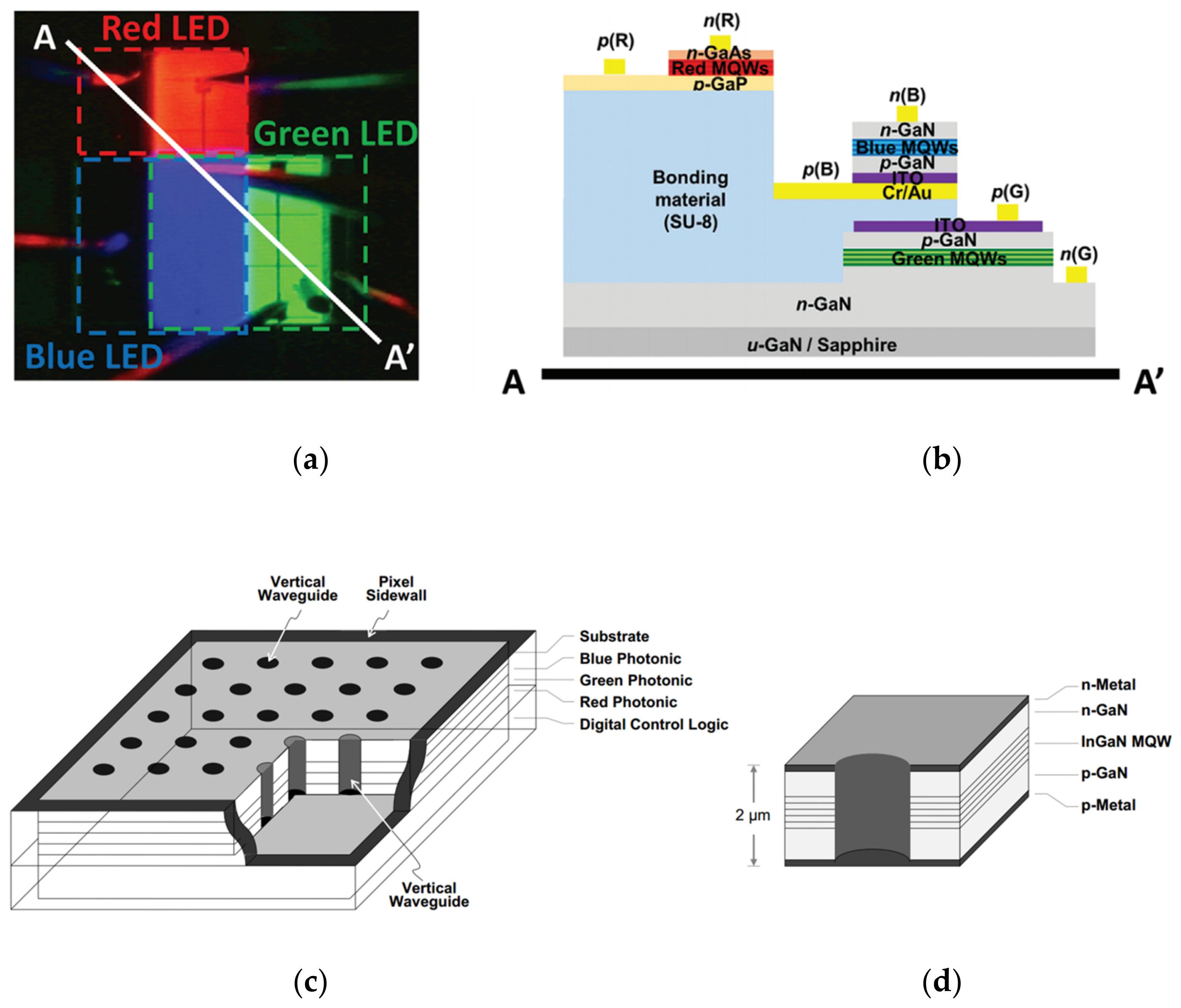
3.2. Monolithic Integration

Heterogeneous integration method makes it possible to manufacture wafer-level electronic system, which is composed of different materials with specific functions and uses a manufacturing process compatible with casting [81,82].
Some researchers have used InGaN/GaN LED chips and vertical metal oxide semiconductor field effect transistors (VMOSFET) or AlGaN/GaN heterojunction field effect transistors (HFET) to achieve monolithic integration [83,84], as shown in Figure 8. In addition, there is a lateral monolithic integration technology that selectively removes the HFET structure and then selectively grows the LED chip structure on the n-GaN buffer layer [85], and a lateral monolithic integration technology that selectively removes the LED chip structure and then selectively grows the MOSFET on the n-GaN layer [86].
Hwangbo et al., directly synthesized MoS2 thin films on GaN-based epitaxial wafers to form thin film transistor arrays. Subsequently, the MoS2 thin film transistor and the Micro-LED device are monolithically integrated to make the AM Micro-LED display. The experimental results show that MoS2 transistor is suitable for the reliable production of large-area Micro-LED display. Although its carrier mobility is relatively low compared with α-Si, low temperature polysilicon (LTPS) and oxide semiconductor, it provides convenience and scalability advantages for the integration process [82]. The University of Sheffield reported a monolithic integrated Micro-LED/high electron mobility transistors (HEMTs) display [87,88]. Firstly, SiO2 mask was grown on AlGaN/GaN heterogeneous crystal wafer by PECVD. Then, the SiO2 mask is selectively etched to the surface of the HEMT template by photolithography and dry etching process to form ordered micropores with a diameter of 20 μm. Next, the Micro-LED structure is selectively grown on the pattern template. Finally, 150 nm p-GaN was grown. Because of the dielectric mask, the growth of LED is limited in the prefabricated SiO2 micro-holes, and Micro-LED with regular arrangement is naturally formed. The growth integration scheme eliminates the dependence on heterogeneous integration to a certain extent, and makes Micro-LED and their drivers compatible on the same GaN platform, which provides an idea for realizing high-performance active matrix Micro-LED displays based on all gallium nitride [50].
In addition to the use of III-nitrides, which are excellent materials for LEDs and transistors, there are also monolithic integrations using Si-based semiconductors. Toyohashi University of Technology Tsuchiyama et al., used Si n-MOSFET and Micro-LED chips for monolithic integration. Si-SiO2-GaN LEDs were fabricated by the surface activated bonding (SAB) method, using a CMOS-compatible process to fabricate Si-MOSFETs on GaN-based LEDs with SiO2 [89]. Vincent Lee etc. of Lumiode company in the US integrated Micro-LED chip and Si TFT on a single chip, and the difficulty was to construct a high-performance low-temperature transistor process. They realized this process by using laser crystallization to convert amorphous silicon with low electron mobility into polysilicon with high mobility [55]. Due to the incompatibility between Micro-LED chip and driving IC process in monolithic integration, another integration method is to manufacture Micro-LED chip array based on group III nitride and CMOS driving matrix based on Si, and then integrate them to achieve separate addressing.

4. Full Color Display

Full-color display is crucial to the commercialization of Micro-LED display. At present, the main methods to realize full-color display include RGB three-color method, UV (ultraviolet)/Blue (blue) LED + luminescent medium method, lens synthesis method and the method of constructing special structure.

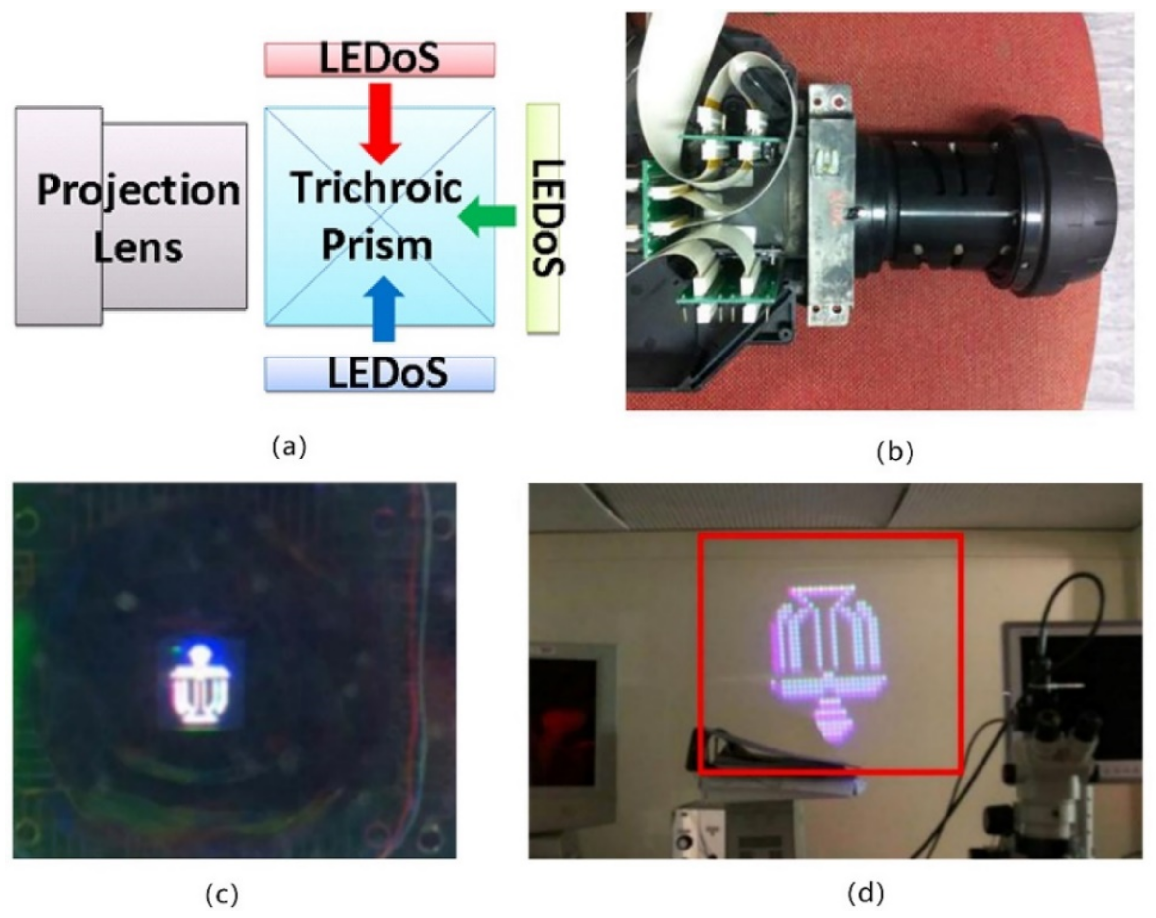
4.1. RGB Three-Color Method

Various colors can be synthesized by mixing RGB three primary colors in a certain proportion. For RGB three primary colors Micro-LED chips, different currents can be passed through to realize color display. The RGB three-primary color method refers to sub-pixels containing three colors of RGB in one pixel. Generally, RGB three-color Micro-LED chips are transferred from their respective growth substrates to the target substrate for assembly by mass transfer, and then full-color display is realized by changing the pulse current period and duty ratio.
It is an ideal implementation scheme to use the same material to form RGB Micro-LED display. Theoretically, these three emission colors can be achieved by changing the indium content in InGaN/GaN MQW LED chips. However, due to the lattice mismatch between the GaN buffer layer and the InGaN quantum well, the emission efficiency of red LED chips based on InGaN/GaN is relatively low. Therefore, red LED chips usually use AlInGaP quaternary materials or GaP/GaAs, but with the size reduced to micron level, the luminous efficiency is not high [90]. By combining blue/green Micro-LED and red OLED to achieve full color, it seems that they can compensate each other’s weaknesses in optical characteristics. However, organic and inorganic LED have different operating mechanisms and device structures, which increases the manufacturing complexity and reduces the scalability and reliability. In addition, the degradation rate between organic and inorganic LED is also different, which affects the reliability of products [3].
In order to improve the quality of color display, Even et al., of Université Grenoble Alpes, France developed a new substrate of InGaNOS. The substrate has a top relaxed InGaN layer, which can be used to grow full-color InGaN LED chips [91]. The process is to first grow an InGaN layer with an initial strain of 200 nm and an indium content of 1.5–8% on a gallium nitride/sapphire substrate. The InGaN layer is then transferred onto the compliant layer of the substrate. Then transfer the patterned InGaN layer to a substrate (sapphire, glass, silicon, etc.) with a size of 300 mm. Experiments show that the photoluminescence spectrum of InGaN structures grown on InGaNOS substrates can range from blue (482 nm) to red (617 nm). By using the substrate with mixed lattice parameters fabricated by this technique, light-emitting chips of different colors can be grown on the same substrate, avoiding mass transfer. In addition, a 100 × 100 μm2 red Micro-LED chip with a light emitting wavelength of 630 nm has also been developed.
Dong-Seon Lee and others developed a method of bonding with SU-8 [92]. Red, green and blue inorganic LED thin films are grown on their respective substrates. When the green LED array is finished, a layer of SU-8 is coated on the wafer and then bonded to the blue LED wafer. The growth substrate can be removed by wet etching. After the blue LED arrays compete, the same process can be used to integrate the red LED wafer. Figure 9a,b are respectively the emission photos of the final full-color sub-pixel and the schematic sectional view of the device structure. The Micro-LED display screen arranged in parallel has a wider color gamut and higher light extraction efficiency. At the same time, bonding integration enables Micro-LED chips to be directly formed on the wafer by photolithography, which is expected to realize Micro-LED display screen with ultra-small pixel size and ultra-high resolution. Although waveguide coupling can effectively eliminate the interference problem, it will reduce the area of the light-emitting active layer, and the limited waveguide cross-sectional area will also reduce the light extraction efficiency [50].
In addition to the method of parallel arrangement of RGB Micro-LED chips to realize full-color display, there is also the method of vertical arrangement. Ostendo uses a new type of spatial light modulator (SLM), namely Quantum Photonic Imager (QPI), Figure 9c,d are structural diagrams of a single QPI pixel and QPI emissive layer respectively. Each QPI pixel consists of a plurality of Micro-LED layers vertically stacked, and each layer generates light with different primary colors (R, G, B). The luminance and chrominance components of each pixel are simultaneously synthesized by digital control logic, which distributes the correct pulse width modulation (PWM) sequence to the Micro-LED chips in the pixel. Moreover, the light emission cone angle can be changed by using the vertical waveguide hole structure, and the emission angle of ±17° to ±45° can be achieved by changing the diameter, depth and spacing of the pixel waveguide [93]. Kang et al., of Gwangju Institute of Science and Technology, Korea, constructed a color-tunable display consisting of an array of blue and green passive Micro-LED chips using a vertical stacking method. The display consists of an 8 × 8 array of Micro-LED chips with chip size and pixel pitch of 75 μm and 100 μm, respectively, and the color of each pixel can be tunable from blue to green (450–540 nm) by applying PWM voltage [94]. The pixel structure based on vertical stacking can reduce the occupied area of the chip, improve the resolution of the display, and is extremely friendly to transparent display. However, this structure is difficult to address every pixel, and the manufacturing process is difficult, so it is necessary to overcome the difficulties of metallization, wiring, driving circuit et al.

4.2. UV/Blue LED + Luminescent Medium Method

Full-color can also be realized by using UV/Blue Micro-LED excitation source with color conversion material [95]. Using fluorescent powder or QDs on the monochromatic Micro-LED chip can realize RGB three primary colors. The resolution of the display prepared by this method is generally high. However, excitation efficiency, material cost and light leakage need to be considered. Compared with the blue light source, the ultraviolet light source has a shorter wavelength, higher luminous efficiency and avoids blue light interference, and is more suitable for use as an excitation source, but the cost of the ultraviolet light source is higher, and the problem of ultraviolet light leakage must be considered. For blue light source, the response time of exciting red light and green light is slower than that of blue light, which makes the response time of pixels different and the intensity of excited light inconsistent, which makes the color distribution uneven [25].
Using the method of color conversion to achieve full color avoids the mass transfer process, and there is no need to prepare the red Micro-LED chip based on AlGaInP, thus avoiding the problems such as brittleness, fast surface recombination and incompatibility with GaN technology [96].
Phosphor materials can excite light with specific wavelength under ultraviolet/blue light source, which has the advantages of high quantum yield, good thermal stability and stable chemical properties. However, due to the large phosphor particles and uneven phosphor layer, the color conversion efficiency and brightness uniformity will be reduced [97]. QD materials are in nanometer scale, which have the advantages of narrow emission spectrum, wide absorption spectrum and high fluorescence intensity, and different colors of emission light can be realized by changing the size of QDs [98]. After the development of CsPbX3 by Kovalenko et al., halide perovskite quantum dots (PQDs) have been widely studied. The band gap of PQDs can be adjusted by changing the composition of X and controlling its size. With the change of X in halogen group from Cl to Br and I, the emission wavelength increases, covering the whole visible light emission range [3]. However, the optical and chemical properties of QDs will change with time, so their stability needs to be improved. Compared with the two conversion materials, QDs materials have certain advantages in Micro-LED display applications.
In 2015, Kuo et al., combined the aerosol jet printing technology with QDs ink, and sprayed QDs of RGB colors on the ultraviolet excitation source, and made a full-color Micro-LED array with chip size of 35 μm and pixel spacing of 40 μm, as shown in Figure 10a. In order to improve the utilization rate of ultraviolet photons, a distributed Bragg reflector is also constructed on the top of the device to reflect the leaked photons to the QDs layer [25].
The uniformity and accuracy of QDs spraying affects the display effect, and to reduce the problem of color crosstalk, Kuo et al., in 2017 combined aerosol jet printing technology with patterned photoresist molds to improve the spraying accuracy of QDs and reduce the optical crosstalk generated between pixels, as shown in Figure 10b. The size of the mold is the same as that of the Micro-LED chip, and the mold can be aligned with the UV Micro-LED chip array. A barrier wall is formed between pixels, so that optical crosstalk is suppressed or eliminated [26]. The color conversion efficiency of Micro-LED displays using QDs is generally low. In order to improve conversion efficiency, contrast and color purity, various methods have been proposed to improve it. For example, Yang et al., of National Taiwan University used Ag nanoparticles to enhance the conversion efficiency of CdSe/ZnS QDs, which made the luminous efficiency of QDs exceed 20% [99]. Chen et al., of National Cheng Kung University in Taiwan spin-coated a patterned black matrix photoresist on the Micro-LED. The black photoresist can block the blue light emitted from the side of the blue Micro-LED excitation source. In order to improve the color purity of red light and green light, a distributed Bragg reflector (DBR) with high reflectivity for blue light and a hybrid Bragg reflector (HBR) that reflects three colors are fabricated on the top and bottom of the QDs Micro-LED chip array, respectively. Through these designs, the contrast ratio of the Micro-LED display has been doubled, and the output intensity of red and green light has also been improved [97]. Gou et al., of University of Central Florida, USA used a funnel tube structure to isolate the Micro-LED chip, which greatly improved the optical efficiency of the Micro-LED chip and eliminated the optical crosstalk. And the light intensity and ambient contrast ratio can be better improved by optimizing the funnel cone angle [100].
Besides aerosol jet printing, the mixture of original solution of QDs and photoresist (QDs-PR) can also be used, and the mixed QDs-PR can be patterned by photolithography process, so as to achieve efficient and large-scale manufacturing. Sharp Company used QDs-PR to convert the color of single blue Micro-LED excitation source, and realized a full-color display with 0.38-inch and 1053 PPI, and its color gamut can reach 120% of sRGB color standard [101]. Liu et al., and others prepared GaN epitaxial layer on Si substrate, and combined with QDs-PR color conversion technology, a full-color micro-display with RGGB color conversion layer with pixel pitch of 80 μm and resolution of 32 × 18 was realized, in which QDs-PR was made by mixing commercial red and green CdSe/ZnS QDs dispersed in toluene with highly transparent negative photoresist. They also added color filters to block unabsorbed blue light, and modified QDs-PR with mixed silica nanospheres to optimize the mixture [102].

4.3. Lens Synehesis Method

Lens synthesis method refers to a method of synthesizing three-color Micro-LED chips into full-color display by using three-way prism. Liu et al., of Hong Kong University of Science and Technology used this method to make a prototype of 3-LEDoS projector. Micro-LED chip array is combined with AM panel fabricated on monocrystalline silicon by flip-chip bonding technology, and red light-emitting chips based on AlGaInP and green and blue light-emitting chips based on GaN on Si substrate are designed and fabricated. Wired and bonded to individual packaging boards, which are connected to the control board, and mounted on the three-way prism to form a full-color projection source, as shown in Figure 11 [103].

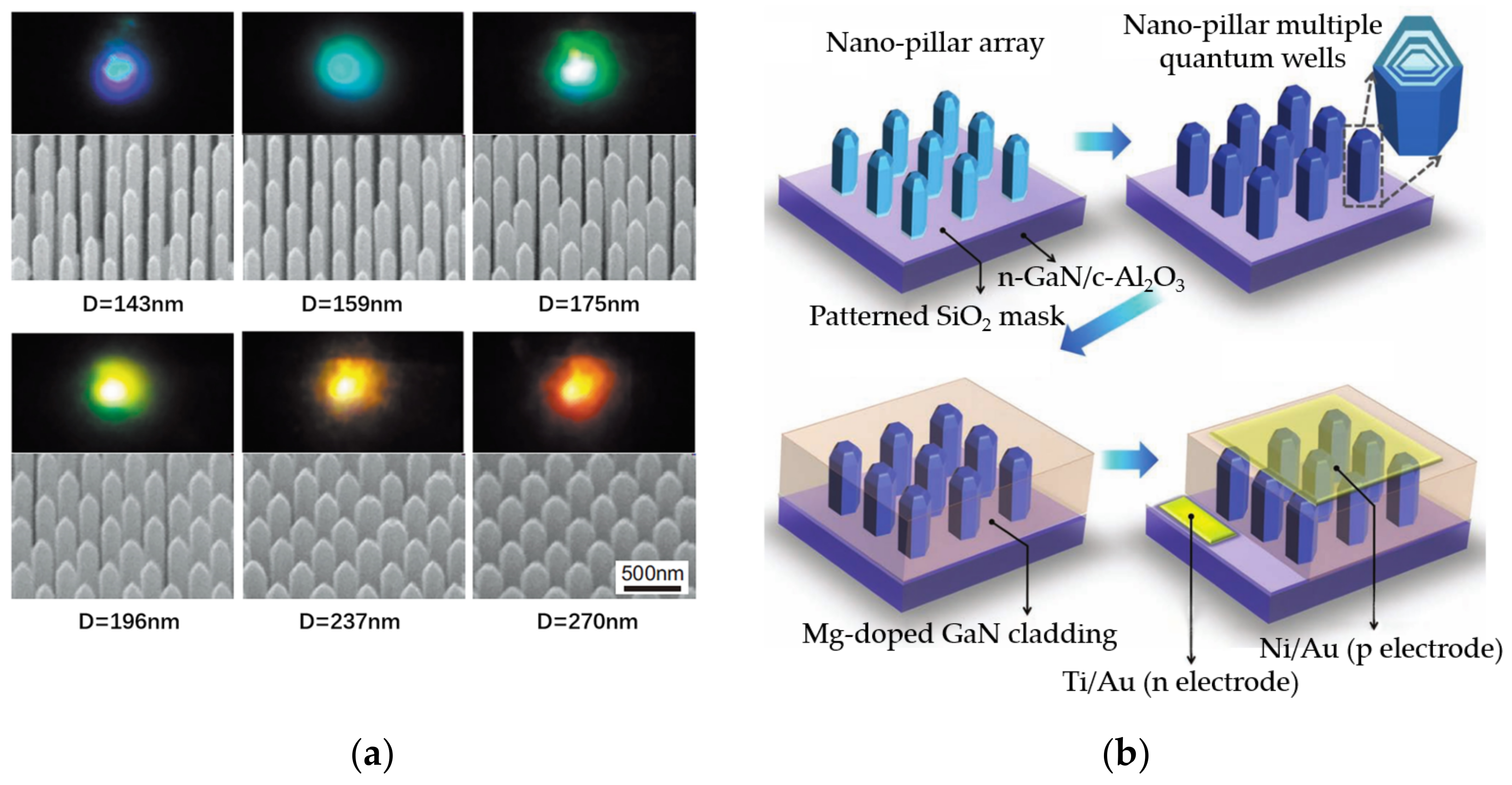
4.4. Special Structure Method

The LED chip structure is usually planar, but the nano-pillar LED chip is different, which has the advantages of small volume, low preparation cost and good luminous performance [104]. Moreover, the lateral restraint of nano-pillar LED chips is much smaller than that of traditional LED chips, which can effectively relax the stress, reduce the dislocation density of GaN and improve the luminous efficiency [105]. InGaN/GaN nano-pillars can be prepared by typical Ti mask selective growth technology, and nano-pillars with different structures correspond to different emitted light [106]. Hiroto et. of Japanese Sophia University used radio-frequency plasma-assisted molecular beam epitaxy (RF-MBE) to epitaxially grow an InGaN/GaN multi-quantum well nano-column array with a diameter of 137–270 nm on the same substrate, and realized the luminescence wavelength from blue to red (479–632 nm). By changing the diameter of the nano-pillars, the indium composition in InGaN is changed, thus changing the emission wavelength, as shown in Figure 12a, which shows the photoluminescence image and scanning electron microscope (SEM) bird’s eye view of the nano-pillar array with a diameter of 143–270 nm [107].
The emission wavelength usually depends on the specific quantum well structure, which is related to the thickness and composition of the quantum well. However, an LED chip structure composed of horizontal and vertical quantum wells proposed by Hong et al., of Seoul National University of Korea can change the emission wavelength by changing the applied bias voltage. Specifically, InxGa1-xN/GaN MQW is uniformly deposited on the tips and sidewalls of the prepared nano-pillars, and then a p-GaN layer is grown on the nano-pillar array, as shown in Figure 12b [108]. Dawson et al., used CMOS with field programmable gate array (FPGA) configuration to drive Micro-LED chip array based on InGaN MQW. The color development principle of this method is similar to that of Hong et al., by changing the bias voltage. The full-color realization principle of the CMOS driving device is to use the competition between piezoelectric field shielding and energy band filling effect to realize red light to green light adjustment by changing the duty ratio [109]. In addition to the above methods, the intermediate carrier barrier layer can be designed to control the current density, so that quantum wells with different in components can realize light emission with specific wavelengths [110], and structures such as hexagonal pyramids, donut-shaped and nano-ring can also be designed to realize different light emission wavelengths [111,112,113,114]. However, these structures are difficult to grow, and it is also a difficult problem to drive the chip. In addition, the luminous area, luminous intensity and color adjustable range need to be considered.

5. Bonding and Driving Technology of Micro-LED Backplane

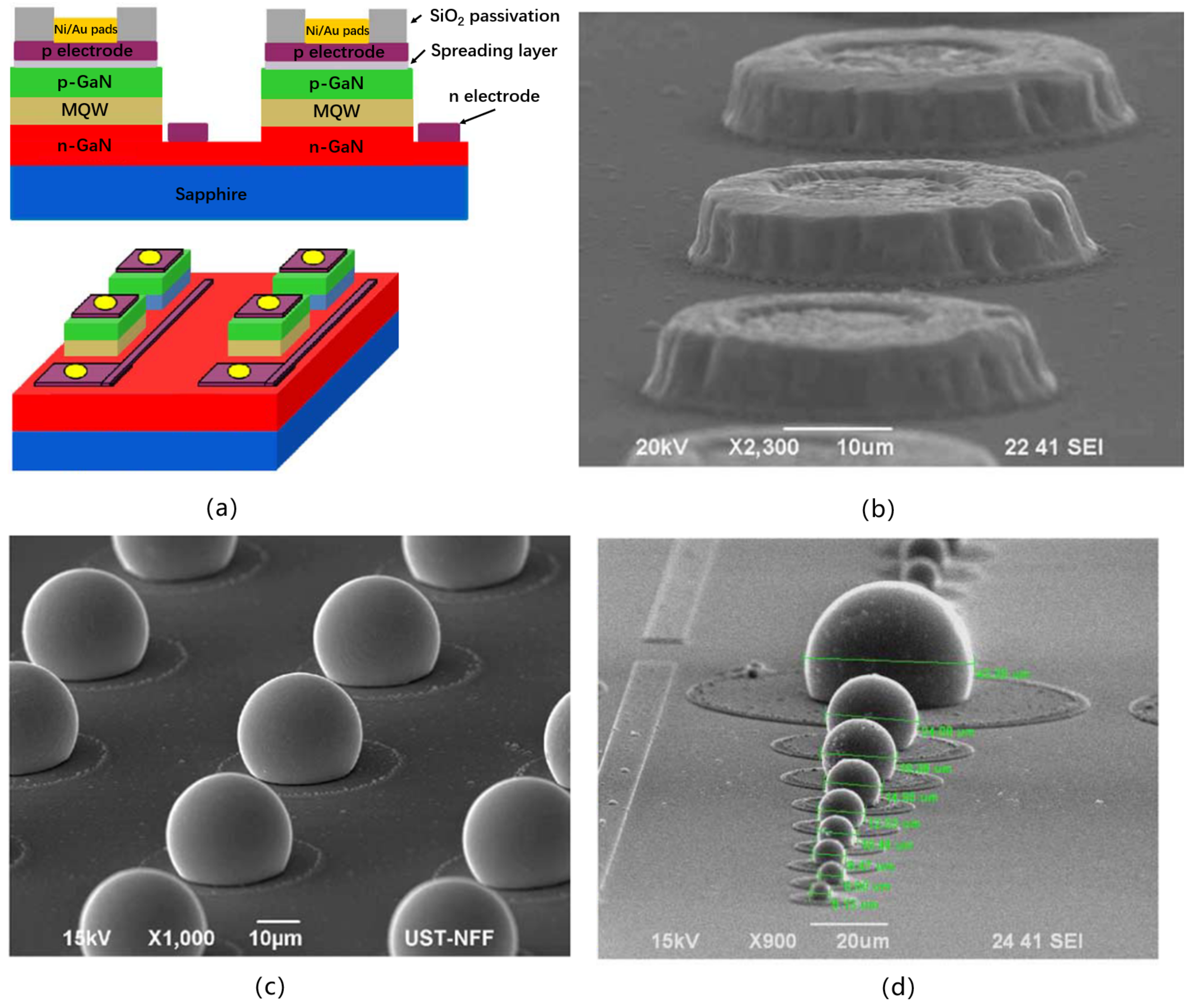
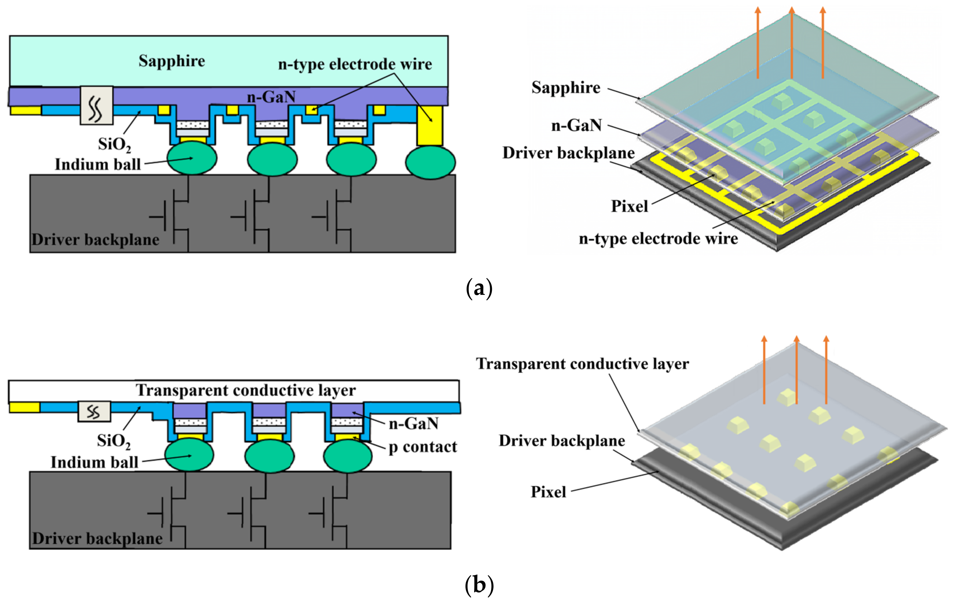
5.1. Bonding Technology

The combination method of driving backplane and Micro-LED chip or epitaxial wafer is mainly divided into chip-level flip-chip bonding and wafer-level combination. Wafer-level combination can be divided into the transfer of Micro-LED epitaxial wafer to Si CMOS and the integration of Micro-LED array and TFT [55,115]. The bonding between Micro-LED epitaxial wafer and Si CMOS backplane is introduced in detail below. Firstly, the Micro-LED epitaxial wafer with eutectic metal layer is combined with CMOS wafer, and the two layers of metal are combined by eutectic bonding process. Then the growth substrate of the epitaxial layer is removed to complete the integration of the Micro-LED epitaxial layer and the CMOS backplane. The next step is to form a Micro-LED array using semiconductor technology, and the metal layer needs to be removed or etched to achieve the isolation and correct connection between the Micro-LED chip and the CMOS chip [116].
For chip-level bonding methods, Micro-LED chips are integrated with CMOS mainly through indium flip-chip, gold flip-chip, microtube flip-chip and gold-free flip-chip bonding [13,23,117,118].
Indium, gold, and gold-free flip-chip bonding methods all belong to metal flip-chip bonding, but the bonding methods are different. For example, the gold bonding layer is generally formed by ultrasonically heating the gold wire, while the indium ball is formed by reflow heating. The following takes indium flip-chip bonding as an example to illustrate the bonding process [23]. The structure of the Micro-LED chip for flip-chip is shown in Figure 13a. First, the photoresist is spin-coated and patterned on the driver backplane, then a 100 nm Ni/Au layer is sputtered as an adhesive layer and a diffusion barrier layer for indium, followed by thermal evaporation to form a 6-μm-thick indium, and the pattern (disk indium) is formed by a photoresist stripping process, as shown in Figure 13b. The disk indium is transformed into spherical indium bumps after annealing in a reflow oven, as shown in Figure 13c. After reflowing, the indium is flip-bonded to the driver backplane using a flip-bonding machine to bond the Micro-LED chip array. Indium bumps of different diameters can be formed by the reflow process, as shown in Figure 13d, where the smallest bump is 5 μm in diameter, which provides a feasible bonding scheme for realizing ultra-high resolution display.
Microtube flip-chip bonding technology can be used to bond Micro-LED chip arrays with a pixel pitch of less than 10 μm. Therefore, this technology can be used to realize high-resolution displays. The technique begins with growing indium solder pads on the Micro-LED chip electrodes, which are fabricated using standard lift-off techniques. Then, a microtube is fabricated on the Si CMOS driving backplane. The fabrication process of the microtube is as follows: firstly, a sacrificial polymer (resin) layer is spin-coated on the driving chip, then the outer shell of the microtube is etched on the contact electrode, then a metal stack with a total thickness of 300 nm is sputtered, and then the inside of the microtube is filled. The metal layer between the filler and the polymer will be protected in the process of reactive ion etching (RIE), while the top metal layer will be etched, and the through hole will be removed by plasma cleaning, which realizes the preparation of microtubes. Align the Micro-LED chip array with Si CMOS, and then insert the microtubules on the electrodes of the Micro-LED chip array, thus completing the bonding process, as shown in Figure 14. The height and diameter of microtubules are determined by the initial polymer lithography step, and the thickness of microtubules is controlled by the parameters related to metal deposition [117].

5.2. Driving Technology
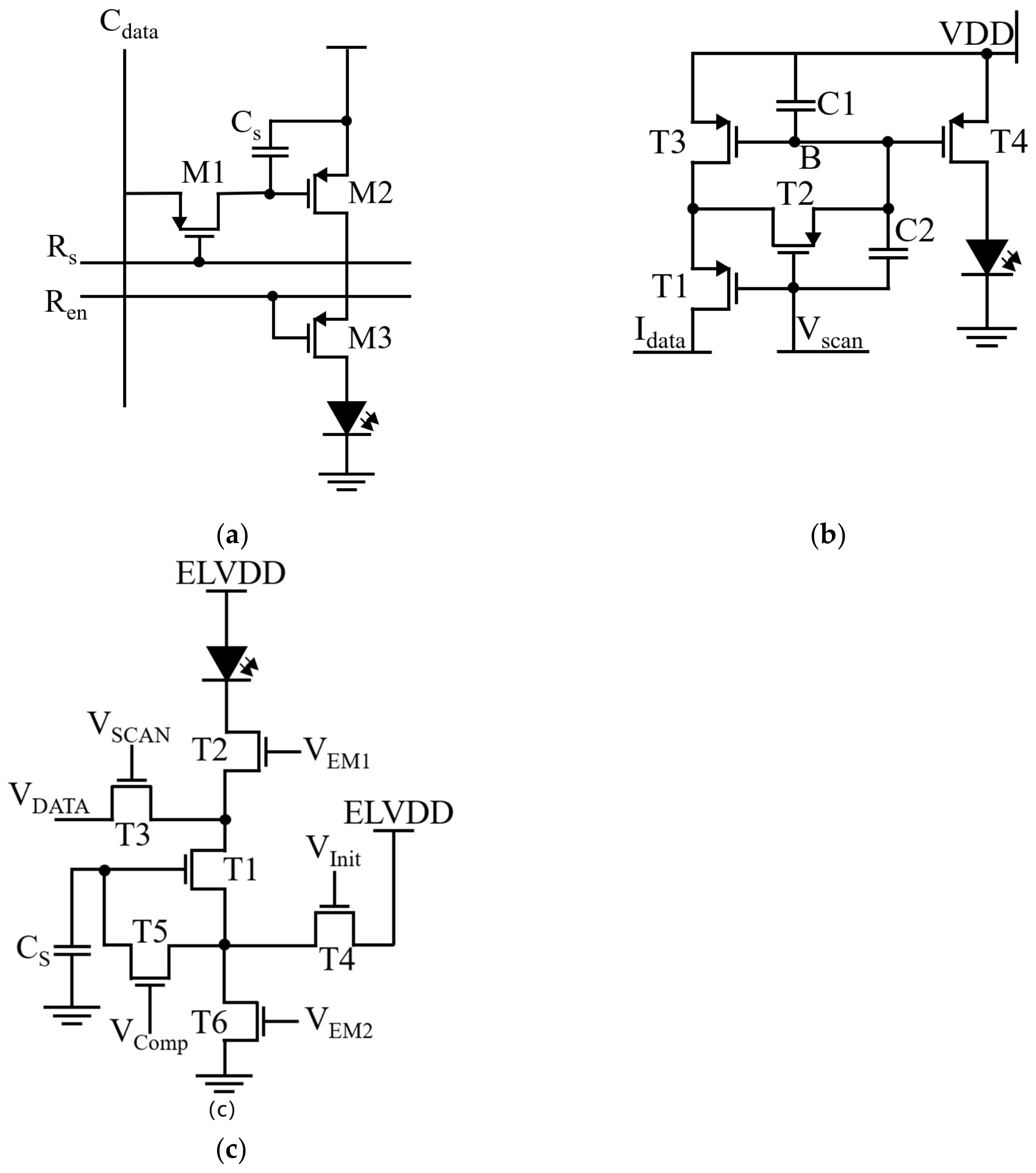
The methods of driving Micro-LED chip (pixel) array are mainly divided into passive matrix (PM) and active matrix (AM). The driving mode will be introduced in detail below.

5.2.1. PM Driving

In the passive driving mode, the pixel electrodes of each row and column are connected to their respective electrode lines, and the lighting is driven by scanning mode. Figure 15 shows the cross-sectional structure and 3D structure of the passive drive array. It can be seen from the figure that deep trenches need to be built between Micro-LED pixels to ensure the isolation of each pixel. However, electrode lines are prone to breakage in deep trenches, resulting in reduced device reliability, and the exposure of the photoresist in the trenches may be insufficient. Therefore, it is generally necessary to use a filler to fill the trench as an insulating layer [119,120].
The external circuit using this driving method is relatively complicated, especially for full-color arrays, because the driving voltages of the three sub-pixels in a pixel are different, so the external circuit will become more and more bulky [121]. In addition, there are obvious deficiencies in passive driving, such as it is not conducive to large-area preparation, the parasitic resistance and capacitance between lines are large, and the pixel gating signal cannot be saved.

5.2.2. AM Driving

In passive driving, the time to gate one line at a time is extremely short, and the pixels in other lines are in the off state, which is different in active driving. The pixels remain in the on state throughout the frame period until their values are updated. That is, in active driving, the on/off state and gray value of each pixel can be controlled independently. Therefore, the AM drive mode has faster refresh rate, higher brightness and less power consumption. Compared with passive driving, active driving is more suitable for large-size, high-resolution and high-performance displays.
Two commonly used structures of active driving are shown in Figure 16. (a) The monolithic integrated structure is shown in Figure 16. This structure only needs to etch the epitaxial moment to n-GaN. The whole Micro-LED chip array is n-GaN, and the current belongs to lateral expansion type, which has good heat dissipation. (b) The figure shows a mass transfer structure, which requires etching the epitaxial layer to the substrate, and then constructing a transparent conductive layer to form a common cathode. The current belongs to the vertical expansion type and has a better current injection effect [120].

CMOS Driving

Metal oxide semiconductor-field effect transistor (MOS-FET), as a technology for fabricating electronic integrated circuits on silicon wafers, is mainly divided into N-type MOS(NMOS) and P-type MOS(PMOS). The 2 transistor 1 capacitor(2T1C) driving circuit commonly used in AM driving has different driving effects for different MOS tubes. As shown in Figure 17, the driving circuits are composed of PMOS and NMOS respectively. Usually, the n contacts of the Micro-LED array are connected together to form a common cathode, and the p contacts are used as independent anodes, because the p layer is generally located on the top of the epitaxial layer, and p-doped GaN has low conductivity, and the Mg dopant has a memory effect. Based on the general structure of Micro-LED pixels, the configuration of common cathode and independent anode mainly supports PMOS active driving; While the independent cathode and common anode configurations support PMOS and NMOS drive circuits. Because the configuration of common cathode and independent anode is usually beneficial to realize aperture ratio, PMOS is widely used in Micro-LED pixel driving. For NMOS, it is more suitable for high-speed applications such as Visible Light Communication (VLC), because the electron mobility in NMOS is several times higher than that in PMOS, so NMOS is much faster. In addition, in the NMOS AM drive circuit, the gate capacitance of the drive transistor and the on-resistance of the transfer transistor are small, so the circuit has a lower RC time constant and a faster switching time [122]. Liou et al., from Taipei Medical University compared the AM drive circuits of PMOS and NMOS, and found that the resistance of PMOS is about three times higher than that of NMOS, so NMOS can be used to reduce the series resistance between Micro-LED pixels [123].

TFT Driving

TFT-driven Micro-LED array is similar to traditional AM-OLED technology, and bonding is usually used to integrate Micro-LED array and TFT-driven backplane. TFT driving technologies mainly include amorphous silicon (α-Si) TFT, LTPS TFT and oxide TFT. α-Si TFT has the advantages of low cost, simple and diverse manufacturing methods, but its carrier mobility is low when applied to high brightness display, and it will face the problems of threshold voltage drift and limited TFT area [124]; However, the carrier mobility of LTPS TFT is several times higher than that of amorphous silicon, so the response speed is faster and the integration degree is higher, and LTPS TFT also has the advantages of low power consumption; Oxide TFT has high carrier mobility, low leakage current, fast response speed and low production cost [125].
The cross-sectional view of a typical flip-chip Micro-LED chip on LTPS TFT is shown in Figure 18, the p electrode of the Micro-LED chip array is connected to the LTPS TFT by solder for independent control, while the n-GaN layer is connected to the common electrode. There is also a stress relief layer and a passivation layer between the Micro-LED chip and the TFT. In order to reduce the contact resistance between the TFT and the chip, the top layer of the chip is an Au layer, and solder is plated on the Au electrodes for bonding. This AM driver enables grayscale control and can be applied to large-scale displays [126].
The preparation process of LTPS TFT technology is mature, but the glass size is limited and the manufacturing cost is high. It is mainly used in small-size display applications, while oxide TFT is more suitable for medium and large-size display applications. Jae et al., of Kyung Hee University in Korea used flip-chip bonding technology to integrate Micro-LED chip array on oxide TFT backplane. Amorphous indium gallium zinc oxide (α-IGZO) TFT-driven backplane was fabricated on glass, and 128 × 384 blue Micro-LED chip array was fabricated on sapphire substrate with chip size of 90 × 50 μm2, while the pixel size of 2T1C driving circuit was 240 × 80 μm2. Figure 19 shows the schematic diagram of bonding between TFT backplane and flip-chip Micro-LED. Figure 19a,b show the cross-sectional views of alignment between n pad and p pad on TFT backplane and electrodes of Micro-LED chip, and the optical diagram of Micro-LED chip prepared on sapphire substrate. Figure 19c shows the process of bonding and lifting the substrate by laser, and the optical diagram of the device with the bonded backplane is shown in Figure 19d. Figure 19e,f are schematic diagrams of bonding the gate and source drivers on the TFT backplane and optical diagrams of bonding devices, respectively. Figure 19g shows the cross-sectional view of the driving pixel. The 2-inch display shown by Jae et al., can display good grayscale images, which shows that oxide TFTs can be used not only for medium and large-size displays, but also for small-size displays [127].

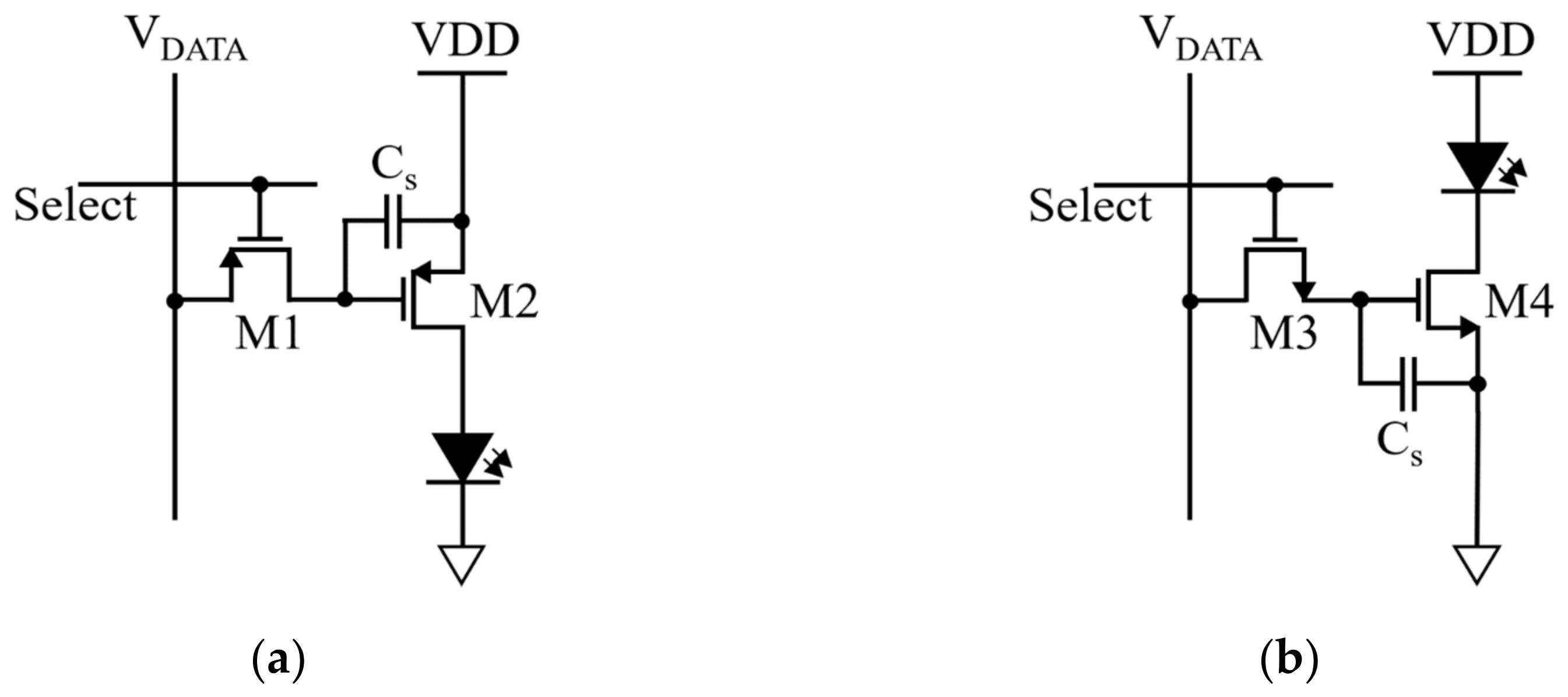
Pixel Driving Circuit

The Micro-LED chip is controlled by transistors, which are mainly divided into voltage drive and current drive. Voltage driving has the advantages of low power consumption and simple pixel driving circuit, but the direct voltage deviation between Micro-LED chips will lead to uneven brightness, and the voltage applied to Micro-LED chips is not linear, which will lead to difficult brightness control. The current drive can linearly control the brightness of the Micro-LED chip. Therefore, it is more suitable to use current driving method for Micro-LED display, but it requires the design and selection of pixel driving circuits. Here are several different pixel driving circuits.
In addition to the typical 2T1C driving circuits [122,127], there are 3T1C, 4T2C, 6T1C and other driving circuits that can drive Micro-LED chips [102,124,128]. Liu et al., used a CMOS backplane to drive a monolithic integrated full-color Micro-LED chip array with QDs-PR for color conversion. The backplane consists of a pixel driver, a scan driver, a data driver and a hybrid regulator. The specific pixel driving circuit includes three transistors and a capacitor, as shown in Figure 20a. Among them, M1 is the scanning switching transistor, M2 is the current source switching transistor, M3 is the row global enable switching transistor, and Cs is the data storage capacitor. When the row scanning signal Rs becomes 0 and the row global enable signal Ren becomes 1, the row scanning process begins: the transistor M1 is turned on, the column data Cdata is written into Cs, and the voltage across Cs is applied to the gate and source of the transistor M2, thus controlling the current applied to the Micro-LED chip. When all column data are sequentially written into the Cs of this row, Rs becomes 1, and the row scanning process moves to the next row. Repeatedly, when all pixels are loaded with display data, Ren is enabled to activate the display [102].
Liu et al., used 4 transistors and 2 capacitors to drive the Micro-LED chip. The specific structure is shown in Figure 20b. T1 and T2 are switching transistors, T3 is a mirror transistor, and T4 is a driving transistor. C1 and C2 are storage capacitors connected in series between the scanning line and VDD. When the scanning signal is applied, T1 and T2 are turned on to charge the capacitor. When the voltage at node B meets the threshold voltage (Vth) requirements of T3 and T4, T3 and T4 are turned on. According to the current mirror principle, the current flowing through the Micro-LED is proportional to Idata. When the scanning signal is applied again, T1 and T2 will be turned off, and the voltage stored in the capacitor will continue to keep T4 on, so that the Micro-LED chip can keep the desired brightness in the frame. This configuration belongs to current drive, the uniformity and display quality of Micro-LED display are better, and better gray scale can be achieved. In addition, two capacitors can adjust the Vth of T3 and T4 more precisely [128].
Shin et al., of Hanyang University in South Korea used the α-IGZO TFT backplane to drive the flip-chip Micro-LED chip array. The specific pixel drive circuit includes 6 transistors and 1 capacitor, as shown in Figure 20c. There are five phases in total, namely, initial phase, compensation phase, emission phase, reset phase and reverse-bias phase. In the first phase, VInit and VComp are at high level, while VSCAN, VEM1 and VEM2 are at low level. ELVDD supplies power to the gate of T1 through the turned-on T4 and T5. In the second phase, VEM1, VEM2, and VInit are at low level, while VComp and VSCAN are at high level. Because the gate of T1 is connected to the data line, the gate voltage of T1 becomes VDATA+Vth, T1. In the third phase, VEM1 and VEM2 are at high level, VInit, VComp and VSCAN are at low level, and the gate and source voltages of T1 are VDATA+Vth, T1 and VDS, T6 respectively, so the gate-source voltages of T1 become VDATA+Vth, T1-VDS, T6. After deduction by Shin et al., it is found that the current flowing through the chip has nothing to do with Vth and T1. In the fourth phase, VEM1, VEM2 and VComp are at high level, while VSCAN and VInit are at low level. The gate of T1 is discharged to ground through T5 and T6, and the drain voltage becomes ELVDD-Vth, LED. In the last phase, VEM1 and VInit are at high level, VSCAN, VEM2 and VComp are at low level, the gate of T1 remains grounded, and the source is charged to ELVDD through T4. At this time, T1 is in a reverse bias state, because the gate-source voltage of T1 is -ELVDD, and the gate-drain voltage is -ELVDD+Vth, LED. The drive circuit with this configuration compensates for the change of Vth and can improve the image quality of the display screen [124].

6. Micro-LED Detection and Repair Technology

Mass transfer technology has made great progress, but there are still some difficulties to overcome for the large-scale manufacturing of Micro-LED displays, such as the yield rate of pixels in the display. For a full-color, full-high-definition (FHD) display, in order to control the number of defective pixels to less than 5, the yield rate must be 99.9999%. However, the generation of bad pixels may occur in various stages of manufacturing, such as the monolithic PM drive array. When the Micro-LED chip array is bonded to the backplane, the uneven bonding between bumps may cause the pixel to be disconnected from the p electrode line, resulting in that the pixel cannot emit light [129]. The residue of photoresist will also affect the yield of the display. Without introducing O2-based plasma ashing step, the yield of Micro-LED chip array with 170 μm mesa gap is about 90%. For the array with 6 μm mesa gap, the yield is about 67%. This is because the photoresist residue leads to problems in the subsequent deposition of SiO2 layer, which makes the element short-circuited. However, after the ashing step is introduced to remove the residual photoresist, the array yield of 170 μm and 6 μm mesa gaps is increased to 100% and 95% respectively [130].
When Micro-LED chips are used for display, the number of chips will reach millions or even tens of millions. Even if the yield is very high, bad spots will exist. Therefore, it is very important for the detection and repair of bad chips. Detection technologies mainly include photoluminescence (PL) detection and electroluminescence (EL) detection. PL detection technology can obtain the brightness and emission wavelength of the chip without touching the chip, but it cannot detect the electrical characteristics of the chip. EL detection can detect the photoelectric characteristics of the chip by contact method, which is more reliable, but electroluminescent detection may damage the chip and the detection efficiency needs to be improved. Due to these shortcomings, the method of combining photoluminescence with other detection technologies is proposed, such as increasing the analysis of scattering spectrum, through which the dislocation density, carrier concentration and etching damage of the chip can be obtained [131,132,133]. A method of using a high-pixel digital camera combined with a microscope system to detect chip brightness has also been proposed. This method can measure the brightness of a single chip to detect defective chips [134]. However, the chip voltage, electrode defects, optical properties, etc. cannot be measured. Therefore, more mature and suitable microarray detection technology has yet to be developed.
For chip repair, the most direct method is to transfer redundant Micro-LED chips [8], as shown in Figure 21, this method will greatly increase the cost of the display. Alternatively, bad pixels can be repaired individually, but this method is also expensive and not suitable for monolithically fabricated displays [61]. Repair technology needs to comprehensively consider factors such as accuracy, repair rate, and cost, and the repair process is closely related to the yield rate during manufacturing. At present, the yield rate of each production link of Micro-LED display is still in the stage to be improved.

7. Commercial Application of Micro-LED

Since the birth of Micro-LED, many investors and companies are making great efforts to develop Micro-LED display technology [4]. In 2012, Sony Corporation of Japan demonstrated the first 55-inch full HD Micro-LED TV, containing more than 6 million Micro-LED chips. Compared with Sony LCD and plasma TVs of the same period, the Micro-LED TV has a contrast ratio 3.5 times higher, a color gamut 1.4 times wider, and a response speed 10 times faster. In 2014, Apple Inc. of the US acquired LuxVue to develop Micro-LED displays suitable for iWatch, iPhone and iMac in the future, which greatly enhanced the popularity and influence of Micro-LED display technology. In 2017, CEA-LETI, a French research institute, demonstrated a prototype of a 10 μm pixel pitch wide video graphics array micro-display based on a patterned Micro-LED array of monochromatic (blue or green) gallium nitride and integrated with CMOS circuits. In 2018, Sony released the giant stitched 16K Micro-LED display "CLEDIS". In the same year, PlayNitride, Taiwan, China, showed two full-color Micro-LED display panel prototypes, a 0.89-inch 64 × 64 resolution panel with a PPI of 105 and a 3.12-inch 256 × 256 resolution panel with a PPI of 116. AUO Corporation of Taiwan, China demonstrated a 12.1-inch full-color Micro-LED display with a pixel size of less than 30 μm, a PPI of 169, and a resolution of 1920 × 720. In 2018, X-Celeprint Company of the US introduced a 5.1-inch full-color Micro-LED display screen, which is composed of 8 × 15 μm red, green and blue LEDs, and a PPI of 70 [29]. In 2018, Samsung of South Korea launched "The Wall", a 146-inch Micro-LED display. In 2019 Ledman, Konka, Leyard and other companies in China launched 324-inch, 236-inch and 135-inch 8K Micro-LED display screens respectively. In 2022, Seoul Viosys of South Korea showed a 54-inch and an 81.5-inch Micro-LED display screen with pixel spacing of 625 μm and 937.5 μm, respectively. Based on the stacked Micro-LED structure, it can be used to manufacture 4K display screens of 100 to 200 inches. In 2023, many companies including Lumiode, Jade Bird Display and Plessey announced that they would launch their products soon.
These developments show that Micro-LED is the next-generation display technology that is generally optimistic. In the future, the application of Micro-LED can be extended from flat panel displays to space displays, wearable/implantable optoelectronic devices, visible light/deep-ultraviolet solar-blind communication, biomedical detection and many other fields [10,13,135,136,137,138,139,140,141,142].

8. Conclusions and Future Developments

This article introduces the research progress of Micro-LED display technology, including key issues such as chip technology, mass transfer and full-color display, and introduces the current targeted solutions. According to the characteristics of Micro-LED displays, the breakthrough for the commercialization of Micro-LED displays is the field of small-size and super-large-size displays, including high-PPI near-eye displays and low-PPI conference walls.
The crystal quality of the epitaxial wafer of Micro-LED chip is directly related to the display effect, and it needs to be optimized from the aspects of emission wavelength, current density and defect density. Miniaturization and thinning make the structure and photoelectric characteristics of Micro-LED chip different from traditional LED and Mini-LED chip. For Micro-LED displays of different sizes, miniaturization and integration methods are mainly divided into mass transfer and monolithic integration. In addition, in view of several mainstream colorization schemes at present, the mass transfer method needs to improve the transfer accuracy and transfer yield to meet the production demand; The emission medium method still needs to solve the problems of conversion efficiency, light leakage and material cost; Lens synthesis method is mainly used in the field of projection; The special structure method also faces the problems of difficult structure growth, high difficulty in driving chips, adjustable color range and so on. For bonding and driving technologies, there are different bonding technologies and driving methods to realize the connection and driving of substrates and Micro-LED chips. As for the bad point of the display, it is necessary to constantly update the detection and repair technology to achieve qualified finished products. In the near future, Micro-LED display technology will enter the public’s field of vision and occupy an essential position in the display field.

Author Contributions

Conceptualization, S.Z. (Shenghao Zhang), H.Z., G.Z., S.Z. (Shaoqiang Zhang), W.X., Z.G. (Zheng Gong), H.N., B.J. and H.L. (Han Lin); methodology, H.Z. and S.Z. (Shenghao Zhang); formal analysis, L.Z., H.L. (Huadan Li), Z.G. (Zhiwen Gao), Y.C. and C.W.; investigation, S.Z. (Shenghao Zhang), H.Z., L.Z., W.L., H.L. (Han Lin), B.J. and T.W.; data curation, W.X., B.J. and H.N.; writing—original draft preparation, S.Z. (Shenghao Zhang), H.Z., L.Z., W.L., H.L. (Han Lin) and B.J.; writing—review and editing, S.Z. (Shenghao Zhang), H.Z., L.Z., W.L., H.L. (Han Lin) and B.J.; visualization, H.Z.; supervision, H.L. (Huadan Li) and W.X.; project administration, H.Z., Z.G. (Zheng Gong) and S.Z. (Shaoqiang Zhang); funding acquisition, H.Z. and W.L. All authors have read and agreed to the published version of the manuscript.

Funding

This research was funded by GuangDong Basic and Applied Basic Research Foundation (grant number: 2020B1515120020), R&D project in key areas of Dongguan City (grant number: 20201200300102) and Dongguan Science and Technology Commissioner Project (grant number: 20221800500192).

Data Availability Statement

Not applicable.

Conflicts of Interest

The authors declare no conflict of interest.

References

  1. Virey, E.H.; Baron, N. 45–1: Status and Prospects of microLED Displays. SID Symp. Dig. Tech. Pap. 2018, 49, 593–596. [Google Scholar] [CrossRef]
  2. Zhou, X.; Tian, P.; Sher, C.-W.; Wu, J.; Liu, H.; Liu, R.; Kuo, H.-C. Growth, transfer printing and colour conversion techniques towards full-colour micro-LED display. Prog. Quantum Electron. 2020, 71, 100263. [Google Scholar] [CrossRef]
  3. Ryu, J.-E.; Park, S.; Park, Y.; Ryu, S.-W.; Hwang, K.; Jang, H.W. Technological Breakthroughs in Chip Fabrication, Transfer, and Color Conversion for High-Performance Micro-LED Displays. Adv. Mater. 2023, 2204947. [Google Scholar] [CrossRef] [PubMed]
  4. Anwar, A.R.; Sajjad, M.T.; Johar, M.A.; Hernández-Gutiérrez, C.A.; Usman, M.; Łepkowski, S.P. Recent Progress in Micro-LED-Based Display Technologies. Laser Photonics Rev. 2022, 16, 2100427. [Google Scholar] [CrossRef]
  5. Parbrook, P.J.; Corbett, B.; Han, J.; Seong, T.Y.; Amano, H. Micro-Light Emitting Diode: From Chips to Applications. Laser Photonics Rev. 2021, 15, 2000133. [Google Scholar] [CrossRef]
  6. Wu, T.; Sher, C.-W.; Lin, Y.; Lee, C.-F.; Liang, S.; Lu, Y.; Huang Chen, S.-W.; Guo, W.; Kuo, H.-C.; Chen, Z. Mini-LED and Micro-LED: Promising Candidates for the Next Generation Display Technology. Appl. Sci. 2018, 8, 1557. [Google Scholar] [CrossRef] [Green Version]
  7. Chen, Z.; Yan, S.; Danesh, C. MicroLED technologies and applications: Characteristics, fabrication, progress, and challenges. J. Phys. D Appl. Phys. 2021, 54, 123001. [Google Scholar] [CrossRef]
  8. Henry, W.; Percival, C. 55–2: Invited Paper: ILED Displays: Next Generation Display Technology. SID Symp. Dig. Tech. Pap. 2016, 47, 747–750. [Google Scholar] [CrossRef]
  9. Horng, R.; Chien, H.; Tarntair, F.; Wuu, D. Fabrication and Study on Red Light Micro-LED Displays. IEEE J. Electron Devices Soc. 2018, 6, 1064–1069. [Google Scholar] [CrossRef]
  10. Liu, Z.; Zhang, K.; Liu, Y.; Yan, S.; Kwok, H.S.; Deen, J.; Sun, X. Fully Multi-Functional GaN-based Micro-LEDs for 2500 PPI Micro-displays, Temperature Sensing, Light Energy Harvesting, and Light Detection. In Proceedings of the 2018 IEEE International Electron Devices Meeting (IEDM), San Francisco, CA, USA, 1–5 December 2018. [Google Scholar]
  11. Paranjpe, A.; Montgomery, J.; Lee, S.M.; Morath, C. 45–2: Invited Paper: Micro-LED Displays: Key Manufacturing Challenges and Solutions. SID Symp. Dig. Tech. Pap. 2018, 49, 597–600. [Google Scholar] [CrossRef]
  12. Zhang, K.; Peng, D.; Lau, K.M.; Liu, Z. Fully-integrated active matrix programmable UV and blue micro-LED display system-on-panel (SoP). J. Soc. Inf. Disp. 2017, 25, 240–248. [Google Scholar] [CrossRef]
  13. Zhang, X.; Li, P.; Zou, X.; Jiang, J.; Yuen, S.H.; Tang, C.W.; Lau, K.M. Active Matrix Monolithic LED Micro-Display Using GaN-on-Si Epilayers. IEEE Photonics Technol. Lett. 2019, 31, 865–868. [Google Scholar] [CrossRef]
  14. Adivarahan, V.; Wu, S.; Sun, W.H.; Mandavilli, V.; Shatalov, M.S.; Simin, G.; Yang, J.W.; Maruska, H.P.; Khan, M.A. High-power deep ultraviolet light-emitting diodes basedon a micro-pixel design. Appl. Phys. Lett. 2004, 85, 1838–1840. [Google Scholar] [CrossRef]
  15. Choi, H.W.; Jeon, C.W.; Dawson, M.D.; Edwards, P.R.; Martin, R.W.; Tripathy, S. Mechanism of enhanced light output efficiency in InGaN-based microlight emitting diodes. J. Appl. Phys. 2003, 93, 5978–5982. [Google Scholar] [CrossRef] [Green Version]
  16. Konoplev, S.S.; Bulashevich, K.A.; Karpov, S.Y. From Large-Size to Micro-LEDs: Scaling Trends Revealed by Modeling. Phys. Status Solidi A 2018, 215, 1700508. [Google Scholar] [CrossRef]
  17. Jin, S.X.; Li, J.; Li, J.Z.; Lin, J.Y.; Jiang, H.X. GaN microdisk light emitting diodes. Appl. Phys. Lett. 2000, 76, 631–633. [Google Scholar] [CrossRef] [Green Version]
  18. Jiang, H.X.; Jin, S.X.; Li, J.; Shakya, J.; Lin, J.Y. III-nitride blue microdisplays. Appl. Phys. Lett. 2001, 78, 1303–1305. [Google Scholar] [CrossRef] [Green Version]
  19. Chan-Wook, J.; Hoi Wai, C.; Gu, E.; Dawson, M.D. High-density matrix-addressable AlInGaN-based 368-nm microarray light-emitting diodes. IEEE Photonics Technol. Lett. 2004, 16, 2421–2423. [Google Scholar]
  20. Griffin, C.; Zhang, H.X.; Guilhabert, B.; Massoubre, D.; Gu, E.; Dawson, M.D. Micro-pixellated flip-chip InGaN and AlInGaN light-emitting diodes. In Proceedings of the Conference on Lasers and Electro-Optics/Quantum Electronics and Laser Science Conference and Photonic Applications Systems Technologies, Baltimore, MD, USA, 6–11 May 2007; Optica Publishing Group: Baltimore, MD, USA, 2007; p. CMF2. [Google Scholar]
  21. Poher, V.; Grossman, N.; Kennedy, G.T.; Nikolic, K.; Zhang, H.X.; Gong, Z.; Drakakis, E.M.; Gu, E.; Dawson, M.D.; French, P.M.W.; et al. Micro-LED arrays: A tool for two-dimensional neuron stimulation. J. Phys. D Appl. Phys. 2008, 41, 094014. [Google Scholar] [CrossRef]
  22. Day, J.; Li, J.; Lie, D.Y.C.; Bradford, C.; Lin, J.Y.; Jiang, H.X. III-Nitride full-scale high-resolution microdisplays. Appl. Phys. Lett. 2011, 99, 031116. [Google Scholar] [CrossRef]
  23. Liu, Z.J.; Chong, W.C.; Wong, K.M.; Lau, K.M. 360 PPI Flip-Chip Mounted Active Matrix Addressable Light Emitting Diode on Silicon (LEDoS) Micro-Displays. J. Disp. Technol. 2013, 9, 678–682. [Google Scholar]
  24. Chong, W.C.; Cho, W.K.; Liu, Z.J.; Wang, C.H.; Lau, K.M. 1700 Pixels Per Inch (PPI) Passive-Matrix Micro-LED Display Powered by ASIC. In Proceedings of the 2014 IEEE Compound Semiconductor Integrated Circuit Symposium (CSICS), La Jolla, CA, USA, 19–22 October 2014; pp. 1–4. [Google Scholar]
  25. Han, H.-V.; Lin, H.-Y.; Lin, C.-C.; Chong, W.-C.; Li, J.-R.; Chen, K.-J.; Yu, P.; Chen, T.-M.; Chen, H.-M.; Lau, K.-M.; et al. Resonant-enhanced full-color emission of quantum-dot-based micro LED display technology. Opt. Express 2015, 23, 32504–32515. [Google Scholar] [CrossRef] [Green Version]
  26. Lin, H.-Y.; Sher, C.-W.; Hsieh, D.-H.; Chen, X.-Y.; Chen, H.-M.P.; Chen, T.-M.; Lau, K.-M.; Chen, C.-H.; Lin, C.-C.; Kuo, H.-C. Optical cross-talk reduction in a quantum-dot-based full-color micro-light-emitting-diode display by a lithographic-fabricated photoresist mold. Photonics Res. 2017, 5, 411–416. [Google Scholar] [CrossRef]
  27. Bai, J.; Cai, Y.; Feng, P.; Fletcher, P.; Zhao, X.; Zhu, C.; Wang, T. A Direct Epitaxial Approach to Achieving Ultrasmall and Ultrabright InGaN Micro Light-Emitting Diodes (μLEDs). ACS Photonics 2020, 7, 411–415. [Google Scholar] [CrossRef] [Green Version]
  28. Shin, J.; Kim, H.; Sundaram, S.; Jeong, J.; Park, B.-I.; Chang, C.S.; Choi, J.; Kim, T.; Saravanapavanantham, M.; Lu, K.; et al. Vertical full-colour micro-LEDs via 2D materials-based layer transfer. Nature 2023, 614, 81–87. [Google Scholar] [CrossRef]
  29. Ding, K.; Avrutin, V.; Izyumskaya, N.; Özgür, Ü.; Morkoç, H. Micro-LEDs, a Manufacturability Perspective. Appl. Sci. 2019, 9, 1206. [Google Scholar] [CrossRef] [Green Version]
  30. Gong, Z.; Jin, S.; Chen, Y.; McKendry, J.; Massoubre, D.; Watson, I.M.; Gu, E.; Dawson, M.D. Size-dependent light output, spectral shift, and self-heating of 400 nm InGaN light-emitting diodes. J. Appl. Phys. 2010, 107, 013103. [Google Scholar] [CrossRef]
  31. Li, C.C.; Zhan, J.L.; Chen, Z.Z.; Jiao, F.; Chen, Y.F.; Chen, Y.Y.; Nie, J.X.; Kang, X.N.; Li, S.F.; Wang, Q.; et al. Operating behavior of micro-LEDs on a GaN substrate at ultrahigh injection current densities. Opt. Express 2019, 27, A1146–A1155. [Google Scholar] [CrossRef]
  32. Zhan, J.; Chen, Z.; Jiao, Q.; Feng, Y.; Li, C.; Chen, Y.; Chen, Y.; Jiao, F.; Kang, X.; Li, S.; et al. Investigation on strain relaxation distribution in GaN-based μLEDs by Kelvin probe force microscopy and micro-photoluminescence. Opt. Express 2018, 26, 5265–5274. [Google Scholar] [CrossRef]
  33. Wong, M.S.; Lee, C.; Myers, D.J.; Hwang, D.; Kearns, J.A.; Li, T.; Speck, J.S.; Nakamura, S.; DenBaars, S.P. Size-independent peak efficiency of III-nitride micro-light-emitting-diodes using chemical treatment and sidewall passivation. Appl. Phys. Express 2019, 12, 097004. [Google Scholar] [CrossRef]
  34. Yang, Y.; Cao, X.A. Removing plasma-induced sidewall damage in GaN-based light-emitting diodes by annealing and wet chemical treatments. J. Vac. Sci. Technol. B Microelectron. Nanometer Struct. Process. Meas. Phenom. 2009, 27, 2337–2341. [Google Scholar] [CrossRef]
  35. Horng, R.-H.; Ye, C.-X.; Chen, P.-W.; Iida, D.; Ohkawa, K.; Wu, Y.-R.; Wuu, D.-S. Study on the effect of size on InGaN red micro-LEDs. Sci. Rep. 2022, 12, 1324. [Google Scholar] [CrossRef] [PubMed]
  36. Yu, J.; Tao, T.; Liu, B.; Xu, F.; Zheng, Y.; Wang, X.; Sang, Y.; Yan, Y.; Xie, Z.; Liang, S.; et al. Investigations of Sidewall Passivation Technology on the Optical Performance for Smaller Size GaN-Based Micro-LEDs. Crystals 2021, 11, 403. [Google Scholar] [CrossRef]
  37. Zhu, J.; Takahashi, T.; Ohori, D.; Endo, K.; Samukawa, S.; Shimizu, M.; Wang, X.-L. Near-Complete Elimination of Size-Dependent Efficiency Decrease in GaN Micro-Light-Emitting Diodes. Phys. Status Solidi A 2019, 216, 1900380. [Google Scholar] [CrossRef]
  38. Usui, A.; Sunakawa, H.; Sakai, A.; Yamaguchi, A. Thick GaN Epitaxial Growth with Low Dislocation Density by Hydride Vapor Phase Epitaxy. Jpn. J. Appl. Phys. 1997, 36, L899–L902. [Google Scholar] [CrossRef] [Green Version]
  39. Templier, F.; Benaïssa, L.; Aventurier, B.; Nardo, C.D.; Charles, M.; Daami, A.; Henry, F.; Dupré, L. 19–6: Invited Paper: A Novel Process for Fabricating High-Resolution and Very Small Pixel-pitch GaN LED Microdisplays. SID Symp. Dig. Tech. Pap. 2017, 48, 268–271. [Google Scholar] [CrossRef]
  40. Chung, K.; Lee, K.; Tchoe, Y.; Oh, H.; Park, J.; Hyun, J.K.; Yi, G.-C. GaN microstructure light-emitting diodes directly fabricated on tungsten-metal electrodes using a micro-patterned graphene interlayer. Nano Energy 2019, 60, 82–86. [Google Scholar] [CrossRef]
  41. Sun, Y.; Yu, T.; Dai, J.; Wang, N.; Luo, R.; Liang, Z.; Zhang, N.; Li, C.; Kang, X.; Zhang, G. Nucleation mechanism of GaN growth on wet etched pattern sapphire substrates. CrystEngComm 2014, 16, 5458–5465. [Google Scholar] [CrossRef]
  42. Hammami, S.; Labchir, N.; Baril, K.; Coulon, P.M.; Alloing, B.; Zuniga Perez, J.; Gourgon, C.; Charles, M.; Dupré, L. Recent micro-LED technology for display applications based on GaN pendeo-epitaxy using SOI nanopillars. In Gallium Nitride Materials and Devices XVIII; SPIE: Bellingham, WA, USA, 2023; Volume PC12421. [Google Scholar]
  43. Aida, H.; Lee, D.S.; Belousov, M.; Sunakawa, K. Effect of Initial Bow of Sapphire Substrate on Substrate Curvature during InGaN Growth Stage of Light Emitting Diode Epitaxy. Jpn. J. Appl. Phys. 2011, 51, 012102. [Google Scholar] [CrossRef]
  44. Aida, H.; Aota, N.; Takeda, H.; Koyama, K. Control of initial bow of sapphire substrates for III-nitride epitaxy by internally focused laser processing. J. Cryst. Growth 2012, 361, 135–141. [Google Scholar] [CrossRef]
  45. Aida, H.; Takeda, H.; Aota, N.; Koyama, K. Reduction of Bowing in GaN-on-Sapphire and GaN-on-Silicon Substrates by Stress Implantation by Internally Focused Laser Processing. Jpn. J. Appl. Phys. 2011, 51, 016504. [Google Scholar] [CrossRef]
  46. Liu, J.; Zhang, J.; Mao, Q.; Wu, X.; Jiang, F. Effects of AlN interlayer on growth of GaN-based LED on patterned silicon substrate. CrystEngComm 2013, 15, 3372–3376. [Google Scholar] [CrossRef]
  47. Nishikawa, A.; Loesing, A.; Slischka, B. 55.1: Invited Paper: Achieving high uniformity of 200 mm GaN-on-Si LED epiwafers for micro LED applications. SID Symp. Dig. Tech. Pap. 2019, 50 (Suppl. S1), 591–594. [Google Scholar] [CrossRef]
  48. White, R.C.; Li, H.; Khoury, M.; Lynsky, C.; Iza, M.; Keller, S.; Sotta, D.; Nakamura, S.; DenBaars, S.P. InGaN-Based microLED Devices Approaching 1% EQE with Red 609 nm Electroluminescence on Semi-Relaxed Substrates. Crystals 2021, 11, 1364. [Google Scholar] [CrossRef]
  49. Beckers, A.; Fahle, D.; Mauder, C.; Kruecken, T.; Boyd, A.R.; Heuken, M. 45–3: Invited Paper: Enabling the Next Era of Display Technologies by Micro LED MOCVD Processing. SID Symp. Dig. Tech. Pap. 2018, 49, 601–603. [Google Scholar] [CrossRef]
  50. Chen, D.; Chen, Y.-C.; Zeng, G.; Zhang, D.W.; Lu, H.-L. Integration Technology of Micro-LED for Next-Generation Display. Research 2023, 6, 0047. [Google Scholar] [CrossRef]
  51. Chen, C.J.; Chen, H.C.; Liao, J.H.; Yu, C.J.; Wu, M.C. Fabrication and Characterization of Active-Matrix 960×540 Blue GaN-Based Micro-LED Display. IEEE J. Quantum Electron. 2019, 55, 3300106. [Google Scholar] [CrossRef]
  52. Soh, M.Y.; Teo, T.H.; Selvaraj, S.L.; Peng, L.; Disney, D.; Yeo, K.S. Heterogeneous Integration of GaN and BCD Technologies. Electronics 2019, 8, 351. [Google Scholar] [CrossRef] [Green Version]
  53. Mukai, T.; Yamada, M.; Nakamura, S. Characteristics of InGaN-Based UV/Blue/Green/Amber/Red Light-Emitting Diodes. Jpn. J. Appl. Phys. 1999, 38, 3976–3981. [Google Scholar] [CrossRef] [Green Version]
  54. Zhang, S.; Zhang, J.; Gao, J.; Wang, X.; Zheng, C.; Zhang, M.; Wu, X.; Xu, L.; Ding, J.; Quan, Z.; et al. Efficient emission of InGaN-based light-emitting diodes: Toward orange and red. Photon. Res. 2020, 8, 1671–1675. [Google Scholar] [CrossRef]
  55. Lee, V.W.; Twu, N.; Kymissis, I. Micro-LED Technologies and Applications. Inf. Disp. 2016, 32, 16–23. [Google Scholar] [CrossRef]
  56. Meitl, M.A.; Zhu, Z.-T.; Kumar, V.; Lee, K.J.; Feng, X.; Huang, Y.Y.; Adesida, I.; Nuzzo, R.G.; Rogers, J.A. Transfer printing by kinetic control of adhesion to an elastomeric stamp. Nat. Mater. 2006, 5, 33–38. [Google Scholar] [CrossRef]
  57. Meng, W.; Xu, F.; Yu, Z.; Tao, T.; Shao, L.; Liu, L.; Li, T.; Wen, K.; Wang, J.; He, L.; et al. Three-dimensional monolithic micro-LED display driven by atomically thin transistor matrix. Nat. Nanotechnol. 2021, 16, 1231–1236. [Google Scholar] [CrossRef]
  58. Makimoto, T.; Kumakura, K.; Kobayashi, Y.; Akasaka, T.; Yamamoto, H. A Vertical InGaN/GaN Light-Emitting Diode Fabricated on a Flexible Substrate by a Mechanical Transfer Method Using BN. Appl. Phys. Express 2012, 5, 072102. [Google Scholar] [CrossRef]
  59. Li, T.; Guo, W.; Ma, L.; Li, W.; Yu, Z.; Han, Z.; Gao, S.; Liu, L.; Fan, D.; Wang, Z.; et al. Epitaxial growth of wafer-scale molybdenum disulfide semiconductor single crystals on sapphire. Nat. Nanotechnol. 2021, 16, 1201–1207. [Google Scholar] [CrossRef]
  60. Feng, X.; Meitl, M.A.; Bowen, A.M.; Huang, Y.; Nuzzo, R.G.; Rogers, J.A. Competing Fracture in Kinetically Controlled Transfer Printing. Langmuir 2007, 23, 12555–12560. [Google Scholar] [CrossRef]
  61. Meitl, M.; Radauscher, E.; Bonafede, S.; Gomez, D.; Moore, T.; Prevatte, C.; Raymond, B.; Fisher, B.; Ghosal, K.; Fecioru, A.; et al. 55–1: Invited Paper: Passive Matrix Displays with Transfer-Printed Microscale Inorganic LEDs. SID Symp. Dig. Tech. Pap. 2016, 47, 743–746. [Google Scholar] [CrossRef]
  62. Cok, R.S.; Meitl, M.; Rotzoll, R.; Melnik, G.; Fecioru, A.; Trindade, A.J.; Raymond, B.; Bonafede, S.; Gomez, D.; Moore, T.; et al. Inorganic light-emitting diode displays using micro-transfer printing. J. Soc. Inf. Disp. 2017, 25, 589–609. [Google Scholar] [CrossRef]
  63. Lee, B.-J.; Khang, D.-Y. Non-deterministic transfer-printing of LED chips with controllable pitch using stretchable elastomeric stamps. Extreme Mech. Lett. 2021, 45, 101287. [Google Scholar] [CrossRef]
  64. Saeidpourazar, R.; Sangid, M.D.; Rogers, J.A.; Ferreira, P.M. A prototype printer for laser driven micro-transfer printing. J. Manuf. Process. 2012, 14, 416–424. [Google Scholar] [CrossRef]
  65. Wartena, R.; Curtright, A.E.; Arnold, C.B.; Piqué, A.; Swider-Lyons, K.E. Li-ion microbatteries generated by a laser direct-write method. J. Power Sources 2004, 126, 193–202. [Google Scholar] [CrossRef]
  66. Choi, M.; Jang, B.; Lee, W.; Lee, S.; Kim, T.W.; Lee, H.-J.; Kim, J.-H.; Ahn, J.-H. Stretchable Active Matrix Inorganic Light-Emitting Diode Display Enabled by Overlay-Aligned Roll-Transfer Printing. Adv. Funct. Mater. 2017, 27, 1606005. [Google Scholar] [CrossRef]
  67. Ezhilarasu, G.; Hanna, A.; Paranjpe, A.; Iyer, S.S. High Yield Precision Transfer and Assembly of GaN µLEDs Using Laser Assisted Micro Transfer Printing. In Proceedings of the 2019 IEEE 69th Electronic Components and Technology Conference (ECTC), Las Vegas, NV, USA, 28–31 May 2019; pp. 1470–1474. [Google Scholar]
  68. Guo, C.; Pan, Z.; Li, C.; Zou, S.; Pang, C.; Wang, J.; Hu, J.; Gong, Z. Large-scale programmable assembly of functional micro-components for advanced electronics via light-regulated adhesion and polymer growth. npj Flex. Electron. 2022, 6, 44. [Google Scholar] [CrossRef]
  69. Pan, Z.; Guo, C.; Wang, X.; Liu, J.; Cao, R.; Gong, Y.; Wang, J.; Liu, N.; Chen, Z.; Wang, L.; et al. Wafer-Scale Micro-LEDs Transferred onto an Adhesive Film for Planar and Flexible Displays. Adv. Mater. Technol. 2020, 5, 2000549. [Google Scholar] [CrossRef]
  70. Inoue, K.; Sugie, R.; Shibamori, T.; Naijo, T.; Endoh, R.; Ushiku, A.; Mori, E. Analysis of micro LED chip after laser transfer. In Proceedings of the 2022 International Conference on Electronics Packaging (ICEP), Sapporo, Japan, 11–14 May 2022; pp. 247–248. [Google Scholar]
  71. Tomoda, K.; Sony Corp. Method of Transferring A Device and Method of Manufacturing A Display Apparatus. US Patent 12/647,826, 29 July 2010. [Google Scholar]
  72. Delaporte, P.; Alloncle, A.-P. [INVITED] Laser-induced forward transfer: A high resolution additive manufacturing technology. Opt. Laser Technol. 2016, 78, 33–41. [Google Scholar] [CrossRef]
  73. Marinov, V.R. 52-4: Laser-Enabled Extremely-High Rate Technology for µLED Assembly. SID Symp. Dig. Tech. Pap. 2018, 49, 692–695. [Google Scholar] [CrossRef]
  74. Henley, F.J. 52-3: Invited Paper: Combining Engineered EPI Growth Substrate Materials with Novel Test and Mass-Transfer Equipment to Enable MicroLED Mass-Production. SID Symp. Dig. Tech. Pap. 2018, 49, 688–691. [Google Scholar] [CrossRef]
  75. Chen, F.; Bian, J.; Hu, J.; Sun, N.; Yang, B.; Ling, H.; Yu, H.; Wang, K.; Gai, M.; Ma, Y.; et al. Mass transfer techniques for large-scale and high-density microLED arrays. Int. J. Extreme Manuf. 2022, 4, 042005. [Google Scholar] [CrossRef]
  76. Wu, Y.; Ma, J.; Su, P.; Zhang, L.; Xia, B. Full-Color Realization of Micro-LED Displays. Nanomaterials 2020, 10, 2482. [Google Scholar] [CrossRef]
  77. Sasaki, K.; Schuele, P.J.; Ulmer, K.; Lee, J.J.; eLux Inc. System and Method for the Fluidic Assembly of Emissive Displays. US Patent 10,418,527, 17 September 2019. [Google Scholar]
  78. Durniak, M.T.; SelfArray Inc. Methods and Systems for Parallel Assembly, Transfer, and Bonding of Ferromagnetic Components. US Patent 15/916,982, 13 September 2018. [Google Scholar]
  79. O’Riordan, A.; Delaney, P.; Redmond, G. Field Configured Assembly: Programmed Manipulation and Self-assembly at the Mesoscale. Nano Lett. 2004, 4, 761–765. [Google Scholar] [CrossRef] [Green Version]
  80. Bibl, A.; Higginson, J.A.; Law, H.-F.S.; Hu, H.-H. Micro Device Transfer Head Heater Assembly and Method of Transferring a Micro Device. US Patent 16/117,414, 30 August 2018. [Google Scholar]
  81. Morikawa, S.; Ueno, K.; Kobayashi, A.; Fujioka, H. Pulsed Sputtering Preparation of InGaN Multi-Color Cascaded LED Stacks for Large-Area Monolithic Integration of RGB LED Pixels. Crystals 2022, 12, 499. [Google Scholar] [CrossRef]
  82. Hwangbo, S.; Hu, L.; Hoang, A.T.; Choi, J.Y.; Ahn, J.-H. Wafer-scale monolithic integration of full-colour micro-LED display using MoS2 transistor. Nat. Nanotechnol. 2022, 17, 500–506. [Google Scholar] [CrossRef]
  83. Lu, X.; Liu, C.; Jiang, H.; Zou, X.; Zhang, A.; Lau, K.M. Monolithic integration of enhancement-mode vertical driving transistorson a standard InGaN/GaN light emitting diode structure. Appl. Phys. Lett. 2016, 109, 053504. [Google Scholar] [CrossRef] [Green Version]
  84. Liu, Z.J.; Huang, T.; Ma, J.; Liu, C.; Lau, K.M. Monolithic Integration of AlGaN/GaN HEMT on LED by MOCVD. IEEE Electron Device Lett. 2014, 35, 330–332. [Google Scholar] [CrossRef]
  85. Liu, C.; Cai, Y.; Zou, X.; Lau, K.M. Low-Leakage High-Breakdown Laterally Integrated HEMT-LED via n-GaN Electrode. IEEE Photonics Technol. Lett. 2016, 28, 1130–1133. [Google Scholar] [CrossRef]
  86. Lee, Y.-J.; Yang, Z.-P.; Chen, P.-G.; Hsieh, Y.-A.; Yao, Y.-C.; Liao, M.-H.; Lee, M.-H.; Wang, M.-T.; Hwang, J.-M. Monolithic integration of GaN-based light-emitting diodes and metal-oxide-semiconductor field-effect transistors. Opt. Express 2014, 22 (Suppl. S6), A1589–A1595. [Google Scholar] [CrossRef] [Green Version]
  87. Cai, Y.; Zhu, C.; Zhong, W.; Feng, P.; Jiang, S.; Wang, T. Monolithically Integrated μLEDs/HEMTs Microdisplay on a Single Chip by a Direct Epitaxial Approach. Adv. Mater. Technol. 2021, 6, 2100214. [Google Scholar] [CrossRef]
  88. Cai, Y.; Haggar, J.I.H.; Zhu, C.; Feng, P.; Bai, J.; Wang, T. Direct Epitaxial Approach to Achieve a Monolithic On-Chip Integration of a HEMT and a Single Micro-LED with a High-Modulation Bandwidth. ACS Appl. Electron. Mater. 2021, 3, 445–450. [Google Scholar] [CrossRef]
  89. Tsuchiyama, K.; Yamane, K.; Sekiguchi, H.; Okada, H.; Wakahara, A. Fabrication of Si/SiO2/GaN structure by surface-activated bonding for monolithic integration of optoelectronic devices. Jpn. J. Appl. Phys. 2016, 55, 05FL01. [Google Scholar] [CrossRef]
  90. Hwang, D.; Mughal, A.; Pynn, C.D.; Nakamura, S.; DenBaars, S.P. Sustained high external quantum efficiency in ultrasmall blue III–nitride micro-LEDs. Appl. Phys. Express 2017, 10, 032101. [Google Scholar] [CrossRef]
  91. Even, A. In Incorporation Improvement in InGaN Based Active Region Using InGaN Pseudo Substrate for Monolithic White LED Application. Ph.D. Thesis, Université Grenoble Alpes, Grenoble, France, 2018. [Google Scholar]
  92. Mun, S.-H.; Kang, C.-M.; Min, J.-H.; Choi, S.-Y.; Jeong, W.-L.; Kim, G.-G.; Lee, J.-S.; Kim, K.-P.; Ko, H.C.; Lee, D.-S. Highly Efficient Full-Color Inorganic LEDs on a Single Wafer by Using Multiple Adhesive Bonding. Adv. Mater. Interfaces 2021, 8, 2100300. [Google Scholar] [CrossRef]
  93. El-Ghoroury, H.S.; Chuang, C.-L.; Alpaslan, Z.Y. 26.1: Invited Paper: Quantum Photonic Imager (QPI): A Novel Display Technology that Enables more than 3D Applications. SID Symp. Dig. Tech. Pap. 2015, 46, 371–374. [Google Scholar] [CrossRef]
  94. Kang, C.-M.; Kong, D.-J.; Shim, J.-P.; Kim, S.; Choi, S.-B.; Lee, J.-Y.; Min, J.-H.; Seo, D.-J.; Choi, S.-Y.; Lee, D.-S. Fabrication of a vertically-stacked passive-matrix micro-LED array structure for a dual color display. Opt. Express 2017, 25, 2489–2495. [Google Scholar] [CrossRef] [PubMed] [Green Version]
  95. Yang, X.; Lin, Y.; Wu, T.; Yan, Z.; Chen, Z.; Kuo, H.-C.; Zhang, R. An overview on the principle of inkjet printing technique and its application in micro-display for augmented/virtual realities. Opto Electron. Adv. 2022, 5, 210123. [Google Scholar] [CrossRef]
  96. Han, J.K.; Choi, J.I.; Piquette, A.; Hannah, M.; Anc, M.; Galvez, M.; Talbot, J.B.; McKittrick, J. Phosphor Development and Integration for Near-UV LED Solid State Lighting. ECS J. Solid State Sci. Technol. 2012, 2, R3138–R3147. [Google Scholar] [CrossRef]
  97. Chen, G.; Wei, B.; Lee, C.; Lee, H. Monolithic Red/Green/Blue Micro-LEDs With HBR and DBR Structures. IEEE Photonics Technol. Lett. 2018, 30, 262–265. [Google Scholar] [CrossRef]
  98. Lee, J.; Sundar, V.C.; Heine, J.R.; Bawendi, M.G.; Jensen, K.F. Full Color Emission from II–VI Semiconductor Quantum Dot–Polymer Composites. Adv. Mater. 2000, 12, 1102–1105. [Google Scholar] [CrossRef]
  99. Wang, Y.-T.; Liu, C.-W.; Chen, P.-Y.; Wu, R.-N.; Ni, C.-C.; Cai, C.-J.; Kiang, Y.-W.; Yang, C.C. Color conversion efficiency enhancement of colloidal quantum dot through its linkage with synthesized metal nanoparticle on a blue light-emitting diode. Opt. Lett. 2019, 44, 5691–5694. [Google Scholar] [CrossRef]
  100. Gou, F.; Hsiang, E.-L.; Tan, G.; Lan, Y.-F.; Tsai, C.-Y.; Wu, S.-T. Tripling the Optical Efficiency of Color-Converted Micro-LED Displays with Funnel-Tube Array. Crystals 2019, 9, 39. [Google Scholar] [CrossRef] [Green Version]
  101. Onuma, H.; Maegawa, M.; Kurisu, T.; Ono, T.; Akase, S.; Yamaguchi, S.; Momotani, N.; Fujita, Y.; Kondo, Y.; Kubota, K.; et al. 25–5: Late-News Paper: 1,053 ppi Full-Color “Silicon Display” based on Micro-LED Technology. SID Symp. Dig. Tech. Pap. 2019, 50, 353–355. [Google Scholar] [CrossRef]
  102. Zhang, X.; Qi, L.; Chong, W.C.; Li, P.; Tang, C.W.; Lau, K.M. Active matrix monolithic micro-LED full-color micro-display. J. Soc. Inf. Disp. 2021, 29, 47–56. [Google Scholar] [CrossRef]
  103. Chong, W.C.; Wong, K.M.; Liu, Z.J.; Lau, K.M. 60.4: A Novel Full-Color 3LED Projection System using R-G-B Light Emitting Diodes on Silicon (LEDoS) Micro-displays. SID Symp. Dig. Tech. Pap. 2013, 44, 838–841. [Google Scholar] [CrossRef]
  104. Kishino, K.; Sakakibara, N.; Narita, K.; Oto, T. Two-dimensional multicolor (RGBY) integrated nanocolumn micro-LEDs as a fundamental technology of micro-LED display. Appl. Phys. Express 2019, 13, 014003. [Google Scholar] [CrossRef]
  105. Guo, W.; Zhang, M.; Banerjee, A.; Bhattacharya, P. Catalyst-Free InGaN/GaN Nanowire Light Emitting Diodes Grown on (001) Silicon by Molecular Beam Epitaxy. Nano Lett. 2010, 10, 3355–3359. [Google Scholar] [CrossRef]
  106. Zhao, S.; Wang, R.; Chu, S.; Mi, Z. Molecular Beam Epitaxy of III-Nitride Nanowires: Emerging Applications from Deep-Ultraviolet Light Emitters and Micro-LEDs to Artificial Photosynthesis. IEEE Nanotechnol. Mag. 2019, 13, 6–16. [Google Scholar] [CrossRef]
  107. Sekiguchi, H.; Kishino, K.; Kikuchi, A. Emission color control from blue to red with nanocolumn diameter of InGaN/GaN nanocolumn arrays grown on same substrate. Appl. Phys. Lett. 2010, 96, 231104. [Google Scholar] [CrossRef]
  108. Hong, Y.J.; Lee, C.-H.; Yoon, A.; Kim, M.; Seong, H.-K.; Chung, H.J.; Sone, C.; Park, Y.J.; Yi, G.-C. Visible-Color-Tunable Light-Emitting Diodes. Adv. Mater. 2011, 23, 3284–3288. [Google Scholar] [CrossRef]
  109. Zhang, S.; Gong, Z.; McKendry, J.J.D.; Watson, S.; Cogman, A.; Xie, E.; Tian, P.; Gu, E.; Chen, Z.; Zhang, G.; et al. CMOS-Controlled Color-Tunable Smart Display. IEEE Photonics J. 2012, 4, 1639–1646. [Google Scholar] [CrossRef] [Green Version]
  110. El-Ghoroury, H.S.; Yeh, M.; Chen, J.C.; Li, X.; Chuang, C.-L. Growth of monolithic full-color GaN-based LED with intermediate carrier blocking layers. AIP Adv. 2016, 6, 075316. [Google Scholar] [CrossRef] [Green Version]
  111. Lee, M.-L.; Yeh, Y.-H.; Tu, S.-J.; Chen, P.C.; Lai, W.-C.; Sheu, J.-K. White emission from non-planar InGaN/GaN MQW LEDs grown on GaN template with truncated hexagonal pyramids. Opt. Express 2015, 23, A401–A412. [Google Scholar] [CrossRef]
  112. Tchoe, Y.; Jo, J.; Kim, M.; Heo, J.; Yoo, G.; Sone, C.; Yi, G.-C. Variable-Color Light-Emitting Diodes Using GaN Microdonut arrays. Adv. Mater. 2014, 26, 3019–3023. [Google Scholar] [CrossRef] [PubMed]
  113. Wang, S.-W.; Hong, K.-B.; Tsai, Y.-L.; Teng, C.-H.; Tzou, A.-J.; Chu, Y.-C.; Lee, P.-T.; Ku, P.-C.; Lin, C.-C.; Kuo, H.-C. Wavelength tunable InGaN/GaN nano-ring LEDs via nano-sphere lithography. Sci. Rep. 2017, 7, 42962. [Google Scholar] [CrossRef] [PubMed] [Green Version]
  114. Zhang, S.; Yan, Y.; Feng, T.; Yin, Y.; Ren, F.; Liang, M.; Wu, C.; Yi, X.; Wang, J.; Li, J.; et al. Wafer-Scale Semipolar Micro-Pyramid Lighting-Emitting Diode Array. Crystals 2021, 11, 686. [Google Scholar] [CrossRef]
  115. Bae, J.; Shin, Y.; Yoo, H.; Choi, Y.; Lim, J.; Jeon, D.; Kim, I.; Han, M.; Lee, S. Quantum dot-integrated GaN light-emitting diodes with resolution beyond the retinal limit. Nat. Commun. 2022, 13, 1862. [Google Scholar] [CrossRef] [PubMed]
  116. Liang, K.-L.; Kuo, W.-H.; Shen, H.-T.; Yu, P.-W.; Fang, Y.-H.; Lin, C.-C. Advances in color-converted micro-LED arrays. Jpn. J. Appl. Phys. 2020, 60, SA0802. [Google Scholar] [CrossRef]
  117. Marion, F.; Bisotto, S.; Berger, F.; Gueugnot, A.; Mathieu, L.; Henry, D.; Templier, F.; Catelain, T. A Room Temperature Flip-Chip Technology for High Pixel Count Micro-Displays and Imaging Arrays. In Proceedings of the 2016 IEEE 66th Electronic Components and Technology Conference (ECTC), Las Vegas, NV, USA, 31 May–3 June 2016; pp. 929–935. [Google Scholar]
  118. McKendry, J. Micro-Pixellated A1InGaN Light-Emitting Diode Arrays for Optical Communications and Time-Resolved Fluorescence Lifetime Measurements. Ph.D. Thesis, University of Strathclyde, Glasgow, UK, 2011. [Google Scholar]
  119. Jeon, C.W.; Choi, H.W.; Dawson, M.D. Fabrication of matrix-addressable InGaN-based microdisplays of high array density. IEEE Photonics Technol. Lett. 2003, 15, 1516–1518. [Google Scholar] [CrossRef]
  120. Guo, W.; Tai, J.; Liu, J.; Sun, J. Process Optimization of Passive Matrix GaN-Based Micro-LED Arrays for Display Applications. J. Electron. Mater. 2019, 48, 5195–5201. [Google Scholar] [CrossRef]
  121. Peng, D.; Zhang, K.; Chao, V.S.; Mo, W.; Lau, K.M.; Liu, Z. Full-Color Pixelated-Addressable Light Emitting Diode on Transparent Substrate (LEDoTS) Micro-Displays by CoB. J. Disp. Technol. 2016, 12, 742–746. [Google Scholar] [CrossRef]
  122. Yeo, K.S.; Ng, W.X.; Soh, M.Y.; Teo, T.H. Micro-LED arrays for display and communication: Device structure and driver architecture. In Proceedings of the 2017 IEEE 12th International Conference on ASIC (ASICON), Guiyang, China, 25–28 October 2017; pp. 993–996. [Google Scholar]
  123. Liou, J.-C.; Yang, C.-F. Design and fabrication of micro-LED array with application-specific integrated circuits (ASICs) light emitting display. Microsyst. Technol. 2018, 24, 4089–4099. [Google Scholar] [CrossRef]
  124. Shin, W.S.; Ahn, H.A.; Na, J.S.; Hong, S.K.; Kwon, O.K.; Lee, J.H.; Um, J.G.; Jang, J.; Kim, S.H.; Lee, J.S. A Driving Method of Pixel Circuit Using a-IGZO TFT for Suppression of Threshold Voltage Shift in AMLED Displays. IEEE Electron Device Lett. 2017, 38, 760–762. [Google Scholar] [CrossRef]
  125. Lin, C.-L.; Chen, F.-H.; Hung, C.-C.; Chen, P.-S.; Deng, M.-Y.; Lu, C.-M.; Huang, T.-H. New a-IGZO Pixel Circuit Composed of ThreeTransistors and One Capacitor for Use in High-Speed-Scan AMOLED Displays. J. Disp. Technol. 2015, 11, 1031–1034. [Google Scholar]
  126. Kim, H.-M.; Um, J.G.; Lee, S.; Jeong, D.Y.; Jung, Y.; Lee, S.H.; Jeong, T.; Joo, J.; Hur, J.; Choi, J.H.; et al. 66–4: High Brightness Active Matrix Micro-LEDs with LTPS TFT Backplane. SID Symp. Dig. Tech. Pap. 2018, 49, 880–883. [Google Scholar] [CrossRef]
  127. Um, J.G.; Jeong, D.Y.; Jung, Y.; Moon, J.K.; Jung, Y.H.; Kim, S.; Kim, S.H.; Lee, J.S.; Jang, J. Active-Matrix GaN µ-LED Display Using Oxide Thin-Film Transistor Backplane and Flip Chip LED Bonding. Adv. Electron. Mater. 2019, 5, 1800617. [Google Scholar] [CrossRef]
  128. Zhang, K.; Liu, Z.; Kwok, H.-S. 25.3: Current Driving Active Matrix Micro-LED Display. SID Symp. Dig. Tech. Pap. 2018, 49 (Suppl. S1), 272–275. [Google Scholar] [CrossRef]
  129. An, C.C.; Wu, M.H.; Huang, Y.W.; Chen, T.H.; Chao, C.H.; Yeh, W.Y. Study on flip chip assembly of high density micro-LED array. In Proceedings of the 2011 6th International Microsystems, Packaging, Assembly and Circuits Technology Conference (IMPACT), Taipei, Taiwan, 19–21 October 2011; pp. 336–338. [Google Scholar]
  130. Xie, E.; Stonehouse, M.; Ferreira, R.; McKendry, J.J.D.; Herrnsdorf, J.; He, X.; Rajbhandari, S.; Chun, H.; Jalajakumari, A.V.N.; Almer, O.; et al. Design, Fabrication, and Application of GaN-Based Micro-LED Arrays with Individual Addressing by N-Electrodes. IEEE Photonics J. 2017, 9, 7907811. [Google Scholar] [CrossRef]
  131. Cunningham, W.; Gouldwell, A.; Lamb, G.; Roy, P.; Scott, J.; Mathieson, K.; Bates, R.; Smith, K.M.; Cusco, R.; Watson, I.M.; et al. Probing bulk and surface damage in widegap semiconductors. J. Phys. D Appl. Phys. 2001, 34, 2748–2753. [Google Scholar] [CrossRef]
  132. Kokubo, N.; Tsunooka, Y.; Fujie, F.; Ohara, J.; Onda, S.; Yamada, H.; Shimizu, M.; Harada, S.; Tagawa, M.; Ujihara, T. Nondestructive visualization of threading dislocations in GaN by micro raman mapping. Jpn. J. Appl. Phys. 2019, 58, SCCB06. [Google Scholar] [CrossRef]
  133. Yamamoto, H.; Agui, K.; Uchida, Y.; Mochizuki, S.; Uruma, T.; Satoh, N.; Hashizume, T. Evaluation of carrier concentration reduction in GaN-on-GaN wafers by Raman spectroscopy and Kelvin force microscopy. Jpn. J. Appl. Phys. 2017, 56, 08LB07. [Google Scholar] [CrossRef] [Green Version]
  134. Zheng, L.; Guo, Z.; Yan, W.; Lin, Y.; Lu, Y.; Kuo, H.C.; Chen, Z.; Zhu, L.; Wu, T.; Gao, Y. Research on a Camera-Based Microscopic Imaging System to Inspect the Surface Luminance of the Micro-LED Array. IEEE Access 2018, 6, 51329–51336. [Google Scholar] [CrossRef]
  135. Herrnsdorf, J.; Wang, Y.; McKendry, J.J.D.; Gong, Z.; Massoubre, D.; Guilhabert, B.; Tsiminis, G.; Turnbull, G.A.; Samuel, I.D.W.; Laurand, N.; et al. Micro-LED pumped polymer laser: A discussion of future pump sources for organic lasers. Laser Photonics Rev. 2013, 7, 1065–1078. [Google Scholar] [CrossRef] [Green Version]
  136. Kim, J.; Gutruf, P.; Chiarelli, A.M.; Heo, S.Y.; Cho, K.; Xie, Z.; Banks, A.; Han, S.; Jang, K.-I.; Lee, J.W.; et al. Miniaturized Battery-Free Wireless Systems for Wearable Pulse Oximetry. Adv. Funct. Mater. 2017, 27, 1604373. [Google Scholar] [CrossRef] [PubMed] [Green Version]
  137. Lee, H.E.; Lee, S.H.; Jeong, M.; Shin, J.H.; Ahn, Y.; Kim, D.; Oh, S.H.; Yun, S.H.; Lee, K.J. Trichogenic Photostimulation Using Monolithic Flexible Vertical AlGaInP Light-Emitting Diodes. ACS Nano 2018, 12, 9587–9595. [Google Scholar] [CrossRef] [PubMed]
  138. Liu, X.; Tian, P.; Wei, Z.; Yi, S.; Huang, Y.; Zhou, X.; Qiu, Z.J.; Hu, L.; Fang, Z.; Cong, C.; et al. Gbps Long-Distance Real-Time Visible Light Communications Using a High-Bandwidth GaN-Based Micro-LED. IEEE Photonics J. 2017, 9, 7204909. [Google Scholar] [CrossRef]
  139. Li, D.; Liu, S.; Qian, Z.; Liu, Q.; Zhou, K.; Liu, D.; Sheng, S.; Sheng, B.; Liu, F.; Chen, Z.; et al. Deep-Ultraviolet Micro-LEDs Exhibiting High Output Power and High Modulation Bandwidth Simultaneously. Adv. Mater. 2022, 34, 2109765. [Google Scholar] [CrossRef]
  140. Ferreira, R.X.G.; Xie, E.; McKendry, J.J.D.; Rajbhandari, S.; Chun, H.; Faulkner, G.; Watson, S.; Kelly, A.E.; Gu, E.; Penty, R.V.; et al. High Bandwidth GaN-Based Micro-LEDs for Multi-Gb/s Visible Light Communications. IEEE Photonics Technol. Lett. 2016, 28, 2023–2026. [Google Scholar] [CrossRef] [Green Version]
  141. Lin, R.; Liu, X.; Zhou, G.; Qian, Z.; Cui, X.; Tian, P. InGaN Micro-LED Array Enabled Advanced Underwater Wireless Optical Communication and Underwater Charging. Adv. Opt. Mater. 2021, 9, 2002211. [Google Scholar] [CrossRef]
  142. Yu, T.-C.; Huang, W.-T.; Lee, W.-B.; Chow, C.-W.; Chang, S.-W.; Kuo, H.-C. Visible Light Communication System Technology Review: Devices, Architectures, and Applications. Crystals 2021, 11, 1098. [Google Scholar] [CrossRef]
Figure 1. The structure and technological process of AlInGaP red vertical Micro-LED array [9].
Crystals 13 01001 g001
Figure 2. Cross-sectional diagram of a flip InGaN Micro-LED bonded to CMOS drive backplane [51].
Crystals 13 01001 g002
Figure 3. 2 μm sidewall defects lead to a significant reduction in the available luminous area.
Crystals 13 01001 g003
Figure 4. Schematic diagram of two methods of mass transfer and monolithic integration [55].
Crystals 13 01001 g004
Figure 5. PDMS transfer process flow diagram. (a) Cover the PDMS on the substrate. (b) Quickly peel the PDMS to peel the chip from the substrate. (c) Print the PDMS with chip on the target substrate. (d) Slowly peel the PDMS to print the chip on the target substrate [56].
Crystals 13 01001 g005
Figure 6. Schematic diagram of non-contact laser micro transfer printing steps: (a) PDMS aligns with and is close to the microstructure devices on the substrate; (b) Microstructure devices transferred to PDMS; (c) Pulse laser heating microstructure device and PDMS interface; (d) Microstructure device transferred to target substrate [64].
Crystals 13 01001 g006
Figure 7. Schematic diagram of fluid transfer [77].
Crystals 13 01001 g007
Figure 8. (a) Schematic diagram of monolithic integrated LED with circular gate VMOSFET [83]; (b) Schematic diagram of monolithic integrated LED of high electron mobility transistor on sapphire substrate [84]. The illustration shows the equivalent circuit diagram of the device.
Crystals 13 01001 g008
Figure 9. (a) Light-emitting microscopic image of full-color sub-pixel; (b) Schematic diagram of device structure section [92]; (c) QPI pixel structure with stacked RGB active layers and vertical waveguides; (d) QPI emission layer structure [93].
Crystals 13 01001 g009
Figure 10. (a) Schematic diagram of aerosol jet printing technology [25]; (b) Schematic diagram of combination of photoresist mold and aerosol jet printing [26].
Crystals 13 01001 g010aCrystals 13 01001 g010b
Figure 11. (a) Schematic diagram of optical structure of projection system; (b) 3-LEDoS projector prototype; (c) White logo formed in prism; (d) 15-inch full color logo projected on the wall [103].
Crystals 13 01001 g011
Figure 12. (a) Photoluminescence images and SEM aerial view of nano-pillar arrays with diameters ranging from 143 nm to 270 nm [107]; (b) Fabrication and electron microscopic image of embedded nano-pillar LED [108].
Crystals 13 01001 g012
Figure 13. (a) Cross section and 3D view of Micro-LED pixels; (b) SEM image of discoid indium; (c) SEM image of indium bump after refluxing process; (d) Indium bumps with different diameters, with a minimum diameter of 5 μm [23].
Crystals 13 01001 g013
Figure 14. (ac) is the process flow of microtubule fabrication; (d) Schematic diagram of microtubule bonding [117].
Crystals 13 01001 g014
Figure 15. Cross-sectional view and 3D structural view of passive drive array [120].
Crystals 13 01001 g015
Figure 16. (a) Cross-sectional view and 3D structure view of monolithic integrated drive array; (b) Cross-sectional view and 3D structural view of the mass transfer drive array [120].
Crystals 13 01001 g016
Figure 17. (a) AM drive circuit configured by PMOS; (b) AM drive circuit configured by NMOS [122].
Crystals 13 01001 g017
Figure 18. Cross-sectional view of TFT driver realized by bump bonding method [126].
Crystals 13 01001 g018
Figure 19. (a) Cross sectional view of alignment between n pad, p pad and Micro-LED chip electrode on TFT backplane. (b) Optical diagram of Micro-LED chip prepared on sapphire substrate. (c) Process of bonding and lifting the substrate by laser. (d) Optical diagram of the device bonded to the backplane. (e,f) Schematic diagram of bonding gate and data driver to TFT backplane and optical diagram of bonding device. (g) Cross sectional view of driving pixels [127].
Crystals 13 01001 g019
Figure 20. (a) Pixel driving circuit of 3T1C [102]. (b) Pixel driving circuit of 4T2C [128]. (c) Pixel driving circuit of 6T1C [124].
Crystals 13 01001 g020
Figure 21. Schematic diagram of dual Micro-LED chip structure.
Crystals 13 01001 g021
Table 1. Comparison of LCD, OLED, and Micro-LED properties [3,5,7].
ItemLCDOLEDMicro-LED
MechanismBacklighting and color filterSelf-emissiveSelf-emissive
Pixel densityMax. 1000 PPIMax. 2500 PPIMax. 30,000 PPI
Brightness<7000 nits<5000 nits>1,000,000 nits
Contrast ratio5000:1>10,000:1>1,000,000:1
Pixel sizeMin. 32 µmMin. 18 µmMin. sub-micrometer
CompactnessLowMediumHigh
Operation temperature−20–80 °C−50–70 °C−100–120 °C
LifetimeLongMediumLong
Response timeLow (ms)Medium (µs)High (ns)
Environmental stabilityHighMediumHigh
Energy consumptionMediumMediumLow
Enhanced functionMediumMediumHigh
FlexibilityLowHighMedium
CostLowLowHigh
Disclaimer/Publisher’s Note: The statements, opinions and data contained in all publications are solely those of the individual author(s) and contributor(s) and not of MDPI and/or the editor(s). MDPI and/or the editor(s) disclaim responsibility for any injury to people or property resulting from any ideas, methods, instructions or products referred to in the content.

