Abstract
Double perovskites are an emerging class of functional materials with a great deal of durability perspective owing to their inherent flexibility in cation coordination selection. Here, we synthesized pristine and Cu2+-doped Ba2NiWO6 utilizing the solid-state reaction route to investigate their structural, morphological, and dielectric behavior. Structural examination revealed the development of a cubic crystal structure for both compositions, and Cu2+ integration in Ba2NiWO6 decreases the crystallite size. The spherical-shaped grains shrink in size and start agglomeration with Cu2+ incorporation. The incorporation of Cu2+ reduces the grain size, leads to accumulation of space charges at the grain boundaries, and thus, facilitates growth in the space charge polarization. This increases the dielectric constant of the material, thus making these compositions viable for advanced miniaturized electronic devices.
1. Introduction
The constantly growing population leads to high demands for energy utilization that are expanding enormously with time. The usage of non-renewable energy sources such as fossil fuels and coal generates CO2 which disrupts the biosphere. Therefore, there is a crucial requirement to develop other cost-effective, non-renewable, and environmentally friendly energy sources. Hydro, wind, nuclear and solar power are considered to be the better alternatives of renewable energy sources [1]. Among these sources, solar power technology has attracted extensive research interest across the globe owing to its eco-friendly nature and easy installation. In addition, it does not involve the emission of any hazardous gases. However, there is the fundamental issue with solar power generation that it cannot work at night time, triggering the need for energy storage devices [2]. At present, batteries, fuel cells, and electrostatic and electrochemical capacitors are commercially available energy storage devices with a limited storage capacity. A large part of ongoing research work is devoted to enhancing the energy storage capacity of these devices. In this regard, dielectric materials are the most promising class of materials that can enhance energy storage capacity, particularly in devices where energy is stored electrostatically [3]. Transition metal oxides in spinels, perovskites, and double perovskite oxides formulations have immense potential as a dielectric materials and have been extensively investigated in the recent past. If these materials possess a higher dielectric constant and lower dielectric loss, they can be utilized in resonators, capacitors, switches, and in all electrical appliances. The high values of dielectric constant and low values of loss are significant conditions for manufacturing elegant and miniaturized devices, provided that the fabricated parts show constant reliability under a wide range of operating temperatures [4].
Among the available potential candidates, double perovskite oxides are a very exciting class because of their wide compositional range and structural flexibility, which make them suitable for a wide spectrum of applications. Double perovskites, which have the general formula A2MM′O6, can accommodate a variety of cations at the A, M and M′ sites such that the overall composition is electrically neutral. They have been a strong focus of research because of their exciting structural and physical characteristics such as magnetic, electrical, photocatalytic, and optical properties. Therefore, materials with the structure of double perovskites possess properties consistent with applications in luminescent, photocatalytic, and dielectric materials [5]. Tungsten-based double perovskites have been the subject of scientific inquiry since 1950. The structural properties of double perovskites have been investigated experimentally using Raman spectroscopy and diffuse reflectance, and theoretically by density functional theory (DFT), and found to be stable. Moreover, the dielectric characteristics of the tungsten-based compositions have been calculated to regulate their capability for microwave and ceramic material applications [6].
In the recent past, researchers devoted their attention to examining the structural, magnetic electric, and multifunctional features of double perovskites in both experimental and theoretical areas. For instance, Hanif et al. studied the cubic double perovskites Sr2XNbO6 (X = La, Lu) using density functional theory (DFT) and investigated their structural, optical, elastic, thermoelectric, and electronic properties by the FP-LAPW approach. It was observed that these compounds are direct bandgap semiconductors with bandgap values of 4.02 eV for Sr2LaNbO6 and 3.7 eV for Sr2LuNbO6 [7]. Similarly, Diao et al. calculated the optical phonons of Ba2MgWO6 (BMWO) utilizing DFT with a local density approach as ab initio mode and presented the vibrational and eigenvector configuration of every mode. The Raman spectra were also analyzed and various modes were identified with the help of first-principle measurements: F2g (1), F2g (2) at 126 cm−1 and 441 cm−1, Eg(O) at 538 cm−1, and A1g(O) at 812 cm−1. FTIR spectra were calculated and fit utilizing three classical parameters and four model features. IR active modes were allocated as F1u (1) at 144 cm−1, F1u (2) at 284 cm−1, F1u (3) at 330 to 468 cm−1 and F1u (4) at 593 to 678 cm−1. The FTIR investigation specified that the F1u (2) mode directed by vibrations of Mg–O6 has a greater impact on the dielectric characteristics of double perovskites [8]. In addition to theoretical investigations, Dehury et al. experimentally studied the structural, morphological, and dielectric characteristics of BiHoCoTiO6 composition. The dielectric behavior exhibited first (Tc1) and second (Tc2) transition temperatures at 175 °C and 325 °C, respectively. The Nyquist plot was modeled with capacitance resistance (CR) equivalent circuit, and various parameters such as bulk or grain, grain boundary, capacitance, and resistance were investigated. The bulk resistance (Rb) reduces considerably when the temperature rises from RT to 300 °C [9]. Likewise, Das et al. examined the structural, dielectric, and magnetic properties of Pr2CoTiO6 material. According to this report, the magnetic calculations below 4 K exposed the antiferromagnetic response in the material, whereas at a Neel temperature (TN) of about 17 K, the value of magnetic moment (µeff) was 6.92 µB. The reported value of the dielectric constant was 45.5 and the loss tangent value was 1.2 [10]. In addition, Vilesh and Subodh synthesized BaBiLiTeO6 and SrBiLiTeO6 double perovskites through a solid-state reaction route and studied the structural, morphological, and dielectric characteristics. They observed that the grain size of the microstructure was 3 µm. At a frequency of 1 MHz, both compounds had porosity-modified dielectric constant. The value for BaBiLiTeO6 was 49.5 and that for SrBiLiTeO6 was 34.4, whereas the value of loss tangent for BaBiLiTeO6 was 0.029 and that for SrBiLiTeO6 was 0.028 [11]. In the report of Coskun et al., iridium (Ir)-substituted LaCrO3 (LCO) was fabricated utilizing a solid-state reaction approach to examine the influence of Ir substitution on ac-conductivity (σac) and dielectric characteristics. It was observed that the value of dielectric constant and conductivity was reduced with the substitution of Ir but with increasing temperature and frequency, the value was increased [12].
In the current study, we elaborate on the dielectric properties of Ba2NiWO6 and Ba2Ni0.5Cu0.5WO6 synthesized by the solid-state reaction method and investigate their structural, morphological and dielectric characteristics as a function of frequency to explore their suitability for energy storage and high-frequency miniaturized electronic devices.
2. Synthesis Method and Characterization Techniques
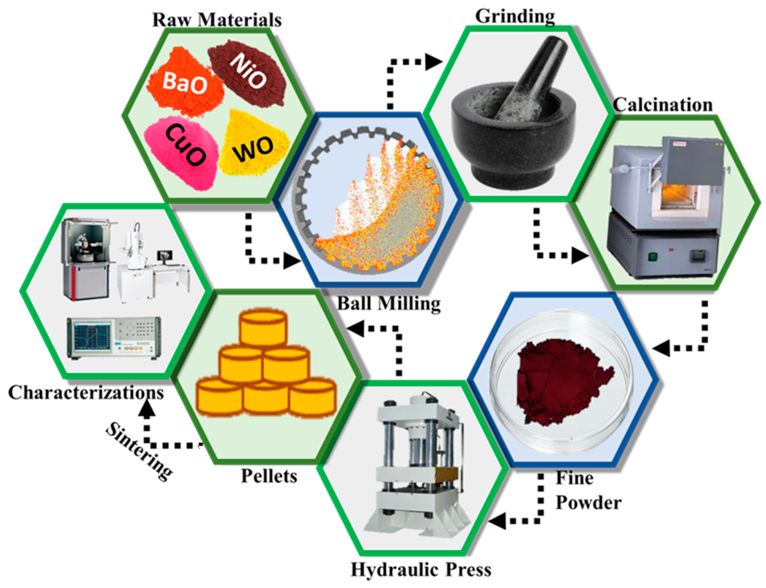
The solid-state reaction approach is versatile in chemical synthesis processes, particularly when the reaction involves oxides as precursors. It is usually assisted by an intermediate and repeated ball milling process. This approach gives high yield, a uniform particle size distribution, fewer impurities and high selectivity of the product. It has been extensively employed for the synthesis of variety of nanomaterials, including spinels, perovskites, and double perovskites. In the present study, this technique was used for the synthesis of Cu-substituted Ba2NiWO6. In this process, BaO (Reagentplus, 99.99%, Saint Louis, MO, USA), NiO (Nanochemazone, 99.99%, Saint Louis, MO, USA), CuO (Sigma Aldrich, 99.99%, Saint Louis, MO, USA), and WO (Sigma Aldrich, 99.99%, Saint Louis, MO, USA) were used as precursors. These precursors were measured according to stoichiometric ratios and mixed by the planetary ball-milling technique at a speed of 500 rev/min to form a homogenous mixture [13]. After that, these materials were ground followed by calcination at 1000 °C for 2 h to obtain the single phase BaNiWO6 and BaNi0.5Cu0.5WO6. Alsabah et al. synthesized A2YVO6 (A = Mg, Sr) double perovskites using solid-state route and investigated their optical behavior through UV-Vis spectroscopy [14]. Similarly, Bharti et al. fabricated Sr2CeSbO6 double perovskites using the same approach and explored the dielectric behavior. Based on the observed value of activation energy, they suggested that this type of behavior is associated with the hopping mechanism of electrons [15]. In addition, Chen et al. in their study, covered most of the chemical approaches which could be employed to synthesize oxides-based double perovskites and highlighted various aspects regarding their applications [16]. These calcined samples were again ground to obtain a fine powder and ultimately transformed to pellet form with a 10 mm diameter and 1.1 mm thickness for different characterizations [17]. Before characterizations, the samples were sintered at 400 °C for 2 h. The schematic of the solid-state reaction method is shown in Figure 1.
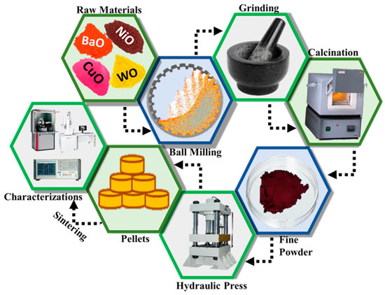
Figure 1.
Schematic of solid-state reaction method.
The structural examination was performed utilizing Rigaku XRD, and the morphological study was carried out using Field Emission Scanning Electron Microscope (FESEM JEOL FESEM (Tokyo, Japan) with Oxford EDX) operated at 5 kV. The dielectric behavior was evaluated using a Precision Impedance Analyzer (PIA).
3. Result and Discussion
3.1. Structural Analysis
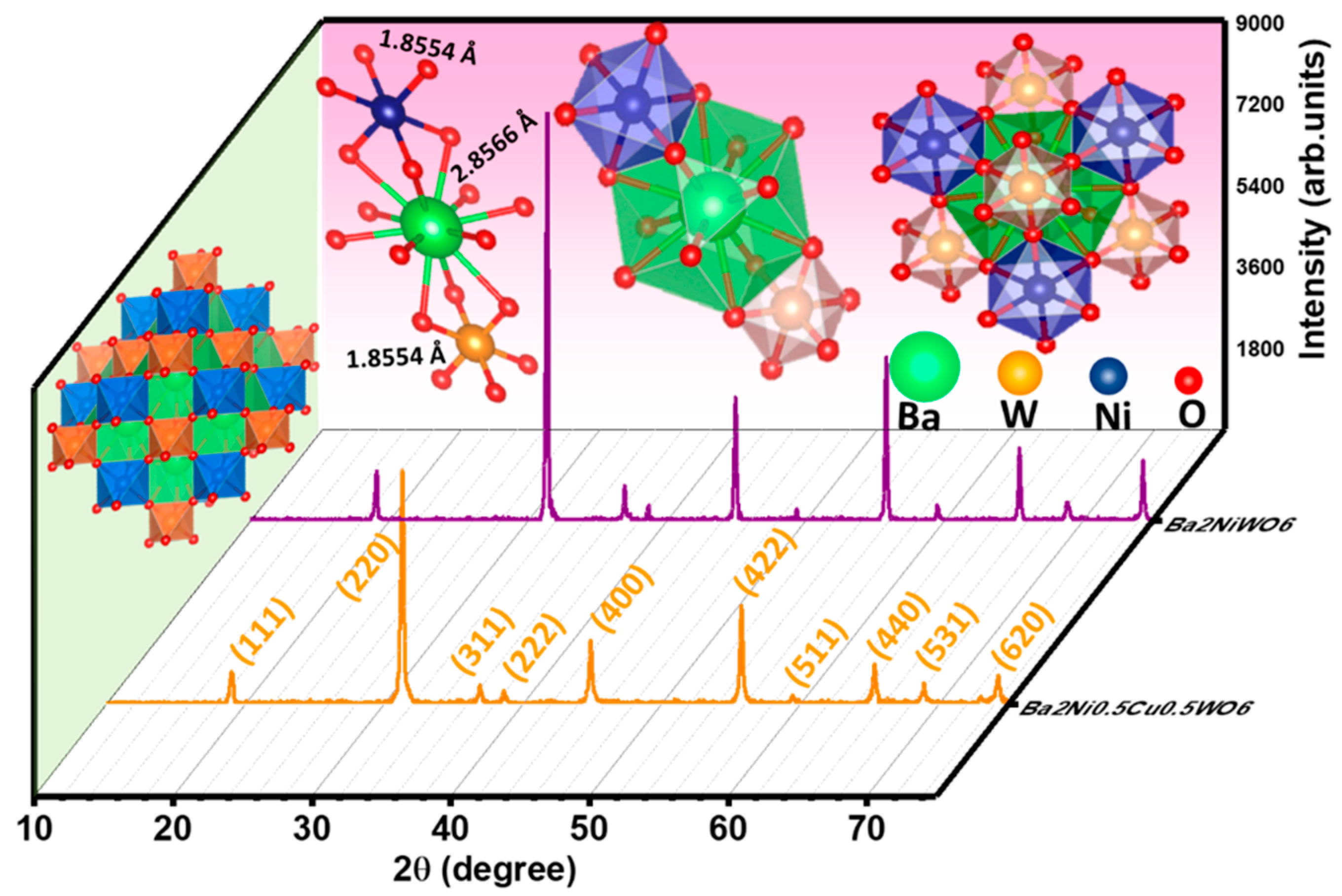
The X-ray diffractograms of the prepared samples of Ba2NiWO6 and Ba2Ni0.5Cu0.5WO6 were used to confirm the development of their cubic double perovskite phases. Figure 2 illustrates the XRD patterns of Ba2NiWO6 and Ba2Ni0.5Cu0.5WO6. It was found that peaks in the XRD pattern of Ba2NiWO6 emerged at 18.93°, 31.16°, 36.71°, 38.40°, 44.64°, 48.90°, 55.44°, 59.13°, 64.98°, 68.35° and 73.82° 2θ values, and these peaks were in good agreement with ICSD card no. 01-073-0135, indicating the formation of a cubic double perovskite phase with space group Fmm [18]. The value of lattice constant (a) calculated from the position of the peaks was determined to be 8.0850 Å. A small shift in the (220) peak towards a smaller 2θ with the incorporation of Cu2+ in the place of Ni2+ is attributed to the larger ionic radius of Cu2+ (0.73Å) as compared with Ni2+ (0.69Å) [19]. This shifting of peaks towards smaller 2θ values reflects the expansion of the unit cell and the value of the lattice parameter for Ba2Ni0.5Cu0.5WO6 to 8.1137 Å [20,21]. The crystallite size (D) was computed using Scherrer’s expression:
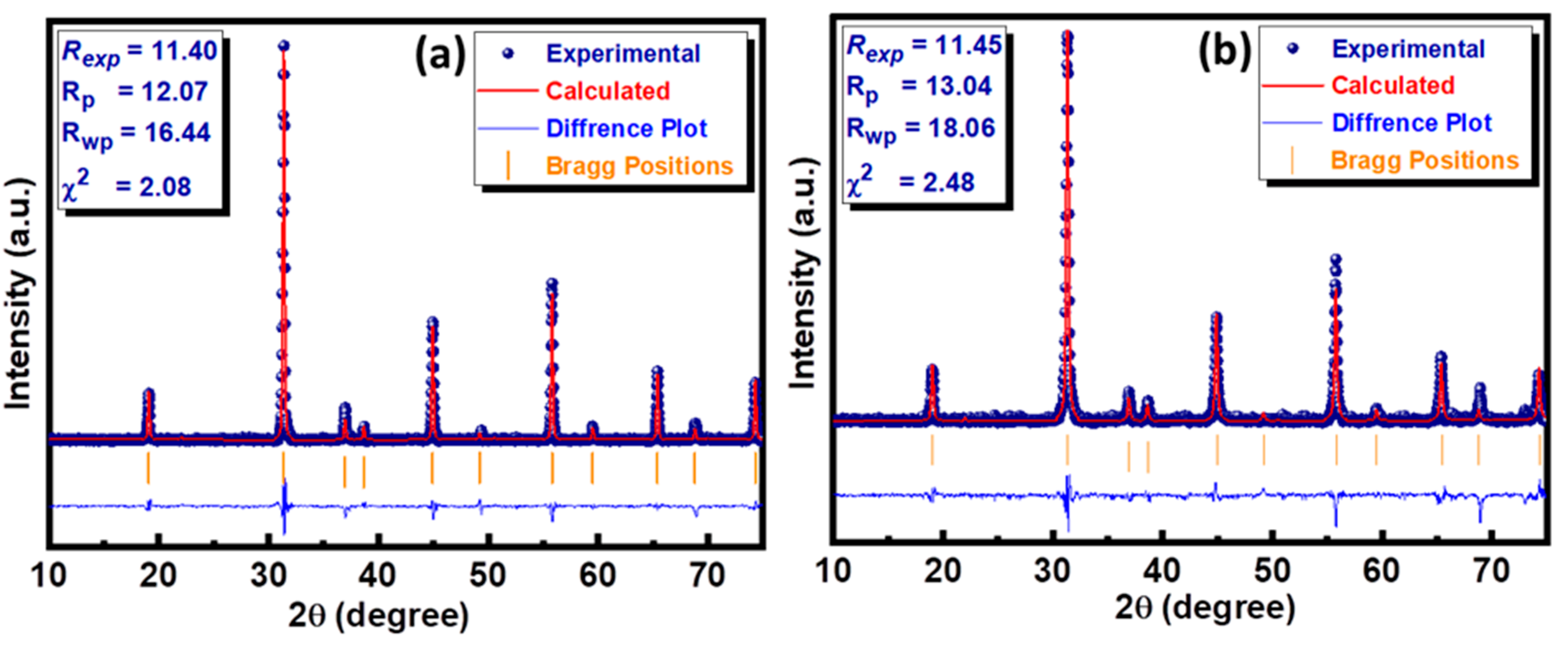
where k is 0.9, which is the shape factor, λ represents the wavelength of CuKα, β signifies the full width at half maximum (FWHM), and θB is the Bragg diffraction angle [22]. The reliability of the crystal structure data was further reinforced by performing the Rietveld refinement using HighScore Plus software. This technique provides a platform to compare the experimental data of the series under investigation with reference data available in the database. This comparison generates a difference plot between experimental and standard data based on the difference in peak position, peak shape, and peak height. This difference is quantified in terms of various residual factors, including the profile factor (Rp), weighted profile factor (Rwp), and expected profile factor (Rexp), to determine the most important factor, the so-called goodness of fit (GoF). The small value of χ2 (<10) indicates the goodness of fit to structural data. The Rietveld refined graphs of both compositions along with their residual factors are presented in Figure 3a,b.

Figure 2.
Indexed XRD patterns of Ba2NiWO6 and Ba2Ni0.5Cu0.5WO6.
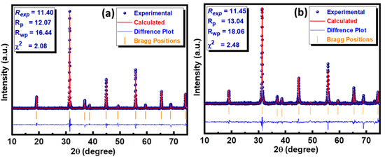
Figure 3.
Rietveld refinement plot of (a) Ba2NiWO6 and (b) Ba2Ni0.5Cu0.5WO6.
3.2. Morphological and Elemental Analysis
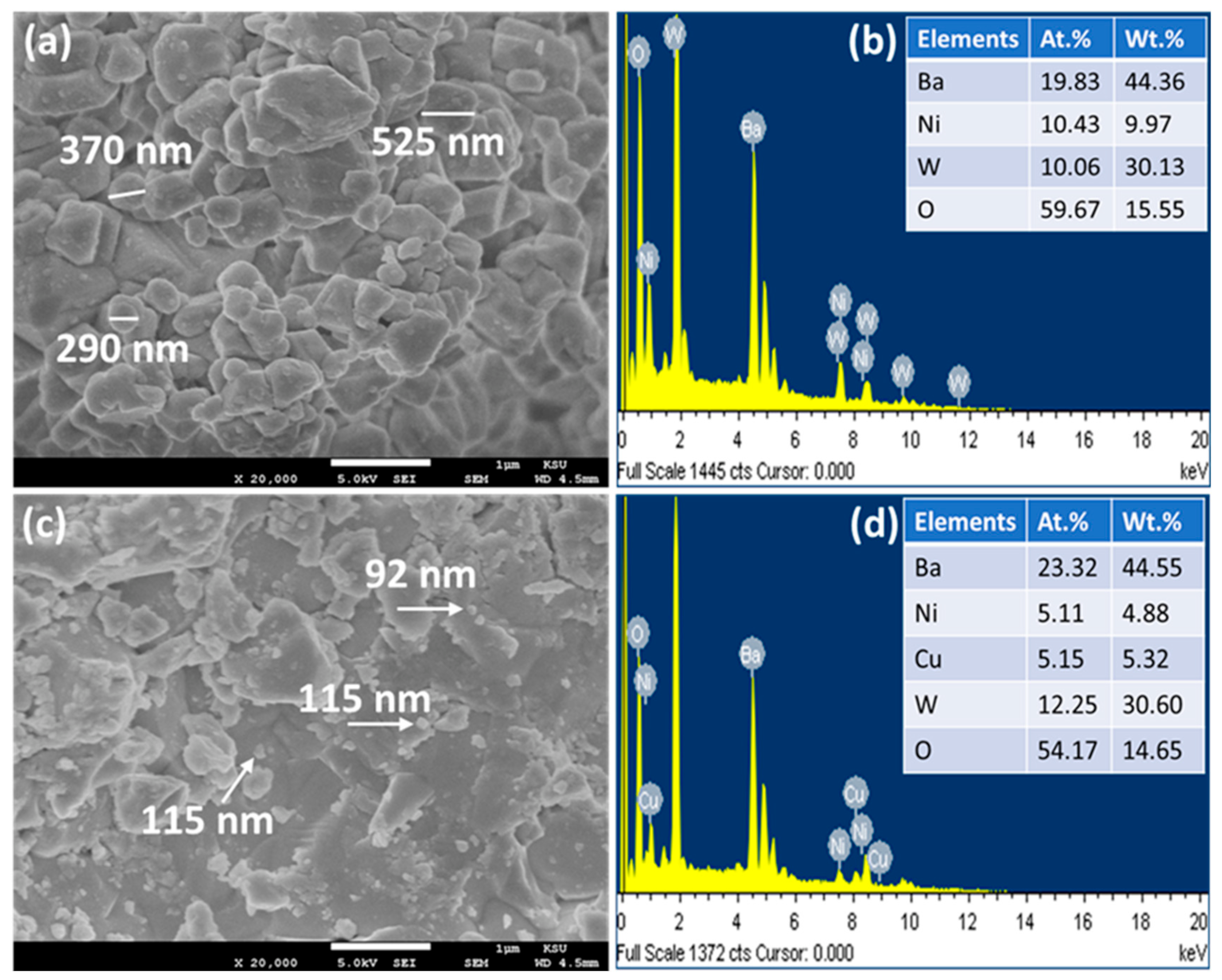
Figure 4a,c illustrate the FESEM images of the Ba2NiWO6 and Ba2Ni0.5Cu0.5WO6 compounds, respectively [23]. The FESEM image of undoped Ba2NiWO6 reveals the well-shaped grains of various sizes stacked over one another. The size of these particles lies in the range of 200–600 nm. The smaller grains are mostly spherical in shape; the medium-sized grains are of oval-shaped, and the larger grains (>400 nm) are of irregular shape. However, these particles are well-connected, leaving behind a very small space between them, which leads to the formation of a quite dense composition that is favorable for better dielectric materials. The incorporation of Cu2+ resulted in a reduction in average grain size owing to the difference in ionic radius of the host and dopant [24]. This mismatching of ionic radius may induce structural deformation, prevent crystal growth, and thus suppress the particle size [25].
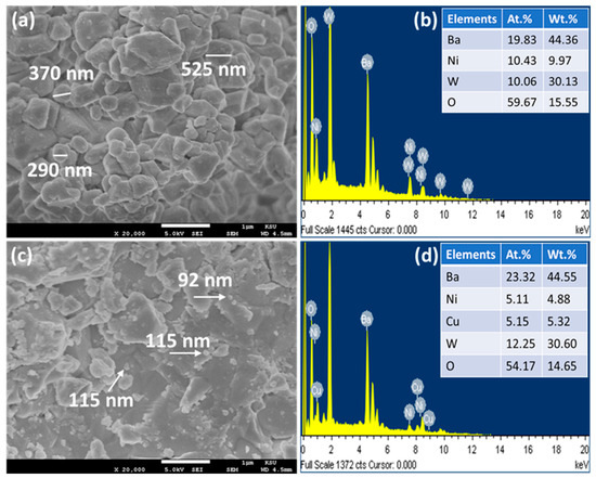
Figure 4.
(a) FESEM image of Ba2NiWO6, (b) EDX spectrum of Ba2NiWO6, (c) FESEM image of Ba2Ni0.5Cu0.5WO6, and (d) EDX spectrum of Ba2Ni0.5Cu0.5WO6.
EDX spectroscopy is a powerful approach and when used in conjunction with SEM, is capable of distinguishing the presence of different elements in any composition by detecting the X-rays emitted from those elements. In addition to the detection of elements, it also helps to quantify these elements. The EDX spectra of Ba2NiWO6 and Ba2Ni0.5Cu0.5WO6 are presented in Figure 4b,d. The presence of Ba, W, Ni, and O in the EDX spectrum of pure Ba2NiWO6 and the presence of Cu in addition to all other elements in the spectrum of Ba2Ni0.5Cu0.5WO6 indicate impurity-free compositions within the detection limit of EDX. The atomic and weight percentage of all involved elements are also incorporated in the EDX spectra and are in good agreement with their stoichiometric formula, thus confirming the formation of the exactly targeted compositions [26].
3.3. Dielectric Properties
The dielectric behaviors of Ba2NiWO6 and Ba2Ni0.5Cu0.5WO6 are controlled by various parameters, including the dispersion of cations, polarization process, and nano-structural configuration. The determined value of parallel capacitance (Cp) was used in relation ε′ = Cpd/Aε0 to compute the real part of the dielectric constant (ε′), where A, d and ε0 represent the area of the pellets, thickness, and permittivity of free space (ε0 = 8.85 × 10¹² F/m), respectively. The equation ε″ = ε′tan δ was used to estimate the imaginary part of the dielectric constant (ε″), where tan δ represents the loss tangent. Figure 5a,b depict the frequency-dependent variation of ε′ and ε″ for Ba2NiWO6 and Ba2Ni0.5Cu0.5WO6, respectively. The values of ε′ and ε″ are greater for Ba2Ni0.5Cu0.5WO6 because, as can be seen in the SEM image of Ba2Ni0.5Cu0.5WO6, the grain size is very small. According to Koop’s theory, the reported dielectric distribution is ascribed to Wagner and Maxwell’s type of interfacial polarization, as the cumulative results of ionic, interfacial, dipolar, and electronic polarizations determine the characteristics such as the dielectric constant [27]. The polarization of space charges at the heterogeneous dielectric structure and grain boundaries are associated with the large values of ε′ and ε″. This polarization is caused by the contaminants, sintering temperature, synthesis methods, grain structure, and pores [28]. The calculated value of ε′ for both compositions at various applied frequencies are presented in Table 1.

Figure 5.
Frequency-dependent variation in (a) real part, (b) imaginary part of dielectric constant, and (c) loss tangent.

Table 1.
Calculated values of the real part of the dielectric constant, imaginary part of the dielectric constant and the loss tangent at various frequencies.
Figure 5c shows how the loss tangent (tan δ) for Ba2NiWO6 and Ba2Ni0.5Cu0.5WO6 samples responds to the applied field with varying frequency. It was calculated using the relation tan δ = 1/2πfRpCp, where 2πf represents the angular frequency (ω), Rp stands for the parallel resistance, and Cp denotes the parallel capacitance. The polarization lags the electric field because of impurities, defects, and grain boundaries, which are linked to the loss tangent. The highest amount of electrical energy is transferred to ions when the vibrational frequency of charge carriers matches the frequency of the electric field; as a result, we can see a power loss peak in Figure 5c. The relation for higher loss in the sample is ωτ = 1, where τ represents relaxation time, which is related to τ = 1/2p as p is the jumping probability per unit time, so ωτ = 1 can also express as ωmax = 2p [29]. It was observed that Ba2NiWO6 and Ba2Ni0.5Cu0.5WO6 exhibited a rapid decrease at frequency 104 Hz, which indicates that at this frequency, the space charge polarization was no longer actively responding to the applied field [30,31].
The complex modulus graph provides significant information on the relaxation property of the material [32]. The following equations were used to calculate the electric modulus’s real part (M′) and imaginary part (M″):
M′ = ε′/(ε′2 + ε″2)
M″ = ε″/(ε′2 + ε″2)
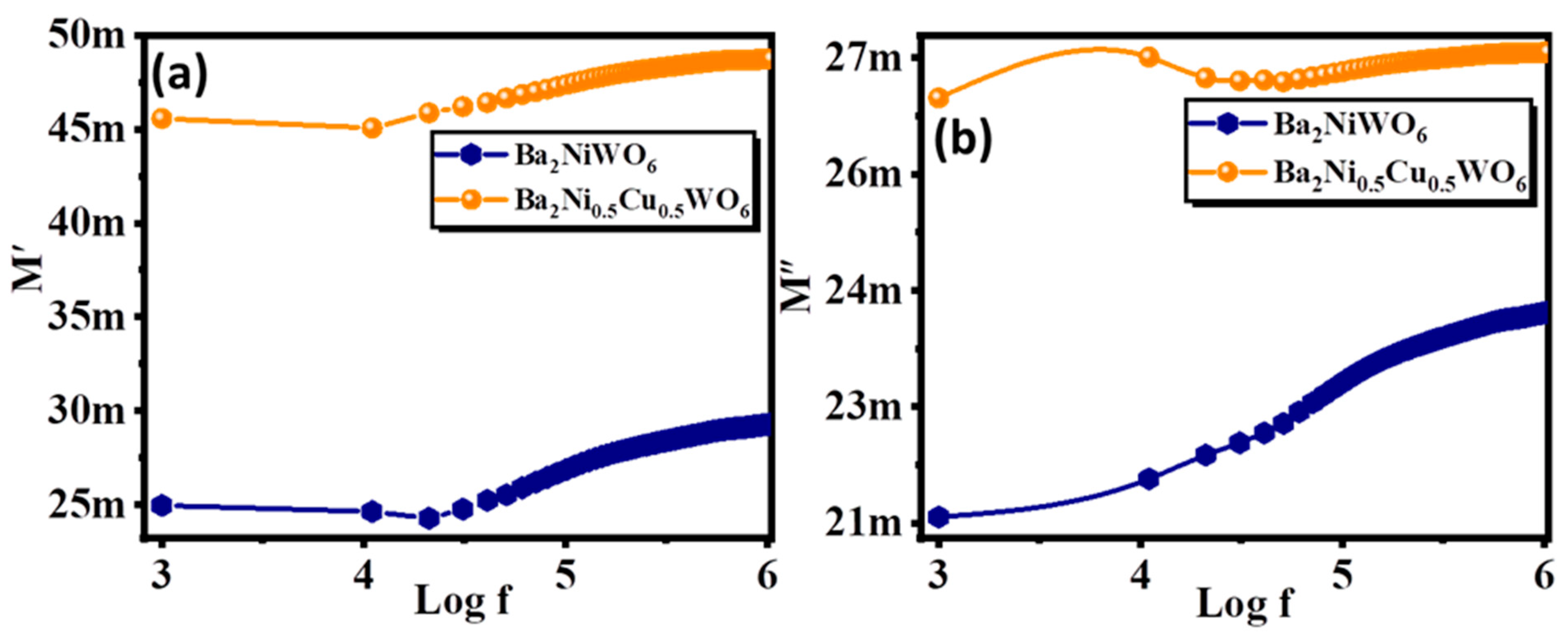
Here, ε′ and ε″ represent the real and imaginary parts of the dielectrics, respectively. The frequency-dependent values of M′ and M″ are displayed in Figure 6a,b. In Figure 6a, the lower values of M′ and M″ are shown in the low-frequency range. Initially, these values were small and started increasing with the increase in frequency, became maximum at a particular frequency and then started declining. Different values of M′ in different frequency ranges reveal the asymmetric behavior of these double perovskites. In addition, the position of the peak in the M″ graph helps to identify the regimes for long-range hopping and short-range hopping, which is a fundamental feature of polycrystalline ceramic material. In the low-frequency range, the charge carriers move over the long-range whereas, in the high-frequency range, charge carriers can only jump to the short-range [33].

Figure 6.
Variation in (a) real part, and (b) imaginary part of modulus with frequency for Ba2NiWO6 and Ba2Ni0.5Cu0.5WO6.
Complex impedance analysis is an interesting and exciting approach to investigating a material’s electrical response to the applied a.c. field in the given frequency range. The measurement of impedance is similar to sensing the material’s accumulative resistive and capacitive response originating from the different intergrain and intragrain nature. The reorientation of dipoles, charge transport, and generation of space charges all are influenced by the frequency of the applied field [34]. The variation of real (Z′) and imaginary (Z″) parts of impedance are presented in Figure 7a,b. The high value of Z′ at low frequency is associated with the accumulation of space charges at the grain boundaries giving rise to the large value of space charge polarization. The value of Z′ decreased with the increase in frequency, which is due to the enhanced conductivity of the materials. The value of Z′ is larger for Ba2Ni0.5Cu0.5WO6 compared with Ba2NiWO6, and this difference is more pronounced in the lower frequency region. This larger value of Z′ for Ba2Ni0.5Cu0.5WO6 is consistent with its morphology. The smaller-sized grains provide more intergrain area and thus provide more resistance to the charge flow. The imaginary part of the impedance is the capacitive reactance of the material, which has an inverse relationship with the frequency of the applied field; therefore, the value of Z″ decreases with an increase in frequency, as shown in Figure 7b.
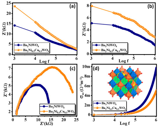
Figure 7.
Variation in (a) real part, (b) imaginary part of impedance with frequency, (c) Nyquist plot, and (d) variation in ac conductivity with frequency for Ba2NiWO6 and Ba2Ni0.5Cu0.5WO6.
Figure 7c illustrates a Nyquist plot, a graph which compares the Z′ and Z″ parts of impedance over a wide frequency range between 1 kHz and 1 MHz. This graph is typically used to explore the electrical characteristics of grain borders and grains. Ba2NiWO6 and Ba2Ni0.5Cu0.5WO6 exhibit non-Debye type relaxation and have a semicircular, curved pattern. Two different types of semicircles can be seen in the Nyquist plot based on the electrical properties of the composition. The first form of a semicircle, which appears at higher frequencies and illustrates the existence of resistance of grains, is also known as a bulk feature. The second semicircle, which appears in the low-frequency range, illustrates the grain boundaries effect [35,36]. The maximum value of Z″ from the topmost region of the semicircle can be used to calculate the capacitance of the respective electroactive regions of the material [37]. The value of resistance offered by these parts can be computed from the x-intercepts of these semicircles. The following relation couples the values of grain boundary resistance (Rgb) resistance and grain boundary capacitance (Cgb):
where ωmax signifies the maximum value of frequency.
ωmaxRgbCgb = 1
The peaks of semicircles are connected to relaxation frequency. At room temperature, the relaxation times (τ) for this composition can be determined by these peaks and can be calculated using the equation:
τ = RgbCgb
However, in the present analysis, we found only one semicircle which matched with the grain boundary, which was significantly affecting the electrical response of fabricated compounds. The maximum diameter of the semicircle of Ba2Ni0.5Cu0.5WO6 demonstrates its highly insulating performance in contrast to other compositions because the resistance parameter for this semicircle is its diameter. However, with Cu2+ substitution, a consistent increase in sample diameter was observed. Additionally, this increase in diameter demonstrates a rise in the resistance of the sample and a decrease in the conductivity [38].
The a.c. conductivity (σac) of Ba2NiWO6 and Ba2Ni0.5Cu0.5WO6 was studied using Josher’s power law. This law is stated as σ(ω) = σac + σo, where the total conductivity of the system is denoted by σ(ω), σac denotes the electrical conductivity which is frequency dependent, and σo indicates the frequency-independent part of the conductivity. Therefore, σac is formulated as σac = ε′ε0ωtan δ, where ε′ is the dielectric constant, ε0 signifies the permittivity of free space, ω denotes the angular frequency, and tan δ represents the loss tangent. Figure 7d displays the frequency-dependent σac responses of Ba2NiWO6 and Ba2Ni0.5Cu0.5WO6. The graphs can be understood on the basis of the polaron mechanism. Because of moving charge carriers, the nearby lattice becomes polarized when an electric field is employed, allowing polarons to originate [39]. Small polarons form when the lattice’s 3-D expansion of distortion or malformation is equal to the order of the lattice constant, and giant polarons appear when the growth of distortion in the 3-D lattice increases after the lattice constant. When σac decreases with an increase in frequency, large polaron transport is used to explain the phenomenon, whereas a small polaron mechanism describes the behavior when it increases with frequency, as in the present study. It is observed that electrical conductivity increases suddenly in the higher frequency range and is nearly constant in the lower frequency range. The small value of σac in the low-frequency range is because of the active nature of grain boundaries here, which results in the large impedance. As a result, it is found that at lower frequency ranges, a.c. conductivity is constant, and then there is a rapid increase observed at higher frequencies [40].
4. Conclusions
In the current report, we synthesized Cu2+-doped Ba2NiWO6 using the solid-state reaction technique. The structural parameters were studied utilizing X-ray diffraction, which confirmed the formation of a double perovskite structure with an expansion of the unit cell and incorporation of Cu at the Ni sites in Ba2NiWO6. The well-shaped distinct grains of pure Ba2NiWO6 with an average grain size of 400 nm were observed, and a considerable decrease in grain size was observed with the incorporation of Cu. The decrease in grain size was associated with an increase in the dielectric constant from 16.3 to 23.4 and an increase in the value of impedance from 14.1 kΩ to 23.5 kΩ at 1k Hz for Ba2NiWO6 and Ba2Ni0.5Cu0.5WO6, respectively. This increase in conductivity provides better control of electronic transport and increases the feasibility of these compositions to be utilized in miniaturized electronic devices. The significant involvement of grain boundaries, detection of the scale of frequency for short-range and long-range hopping mechanisms, and the involvement of small polaron provide a comprehensive understanding of the dielectric and electrical behavior of these compositions and demonstrate their suitability for multiple technological applications.
Author Contributions
S.M.R.; Conceptualization, Methodology, M.H.A.; Software, Data curation, G.M.M.; Visualization, Investigation, and graph plotting, S.S.; Data analysis, S.A. (Shahid Atiq); Supervision, Reviewing and Editing, S.A. (Sikandar Aftab); Final proof read, M.A.E.; Helping in preparing the revision. All authors have read and agreed to the published version of the manuscript.
Funding
The authors would like to acknowledge Researcher’s Supporting Project Number (RSP2023R71), King Saud University, Riyadh, Saudi Arabia.
Data Availability Statement
All data presented in this manuscript will be available on demand.
Acknowledgments
The authors would like to acknowledge Researcher’s Supporting Project Number (RSP2023R71), King Saud University, Riyadh, Saudi Arabia.
Conflicts of Interest
The authors declare that they have no known competing financial interests or personal relationships that could have appeared to influence the work reported in this paper.
References
- Albalawi, H.; Mustafa, G.M.; Saba, S.; Kattan, N.A.; Mahmood, Q.; Somaily, H.H.; Amin, M.A. Study of optical and thermoelectric properties of double perovskites Cs2KTlX6 (X= Cl, Br, I) for solar cell and energy harvesting. Mater. Today Commun. 2022, 32, 104083. [Google Scholar] [CrossRef]
- Najar, F.A.; Abass, S.; Sultan, K.; Kharadi, M.A.; Malik, G.F.A.; Samad, R. Comparative study of optical properties of substitutionally doped La2NiMnO6 double perovskite ceramic: A potential candidate for solar cells and dielectrics. Phys. B Condens. Matter 2021, 621, 413311. [Google Scholar] [CrossRef]
- Winiarski, M.J.; Kozieł, K.; Sadecka, K.; Dereń, P.J. The substitution effects on electronic structure of Ba2MgWO6 double perovskite oxide. Solid State Commun. 2020, 314, 113936. [Google Scholar] [CrossRef]
- Chen, J.W.; Chiou, K.R.; Hsueh, A.C.; Chang, C.R. Dielectric relaxation of the double perovskite oxide Ba2PrRuO6. RSC Adv. 2019, 9, 12319–12324. [Google Scholar] [CrossRef] [PubMed]
- Miniajluk, N.; Bondzior, B.; Stefańska, D.; Dereń, P.J. Eu3+ ions in the highly symmetrical octahedral site in Ba2MgWO6 double perovskite. J. Alloy. Compd. 2019, 802, 190–195. [Google Scholar] [CrossRef]
- Bugaris, D.E.; Hodges, J.P.; Huq, A.; Zur Loye, H.C. Crystal growth, structures, and optical properties of the cubic double perovskites Ba2MgWO6 and Ba2ZnWO6. J. Solid State Chem. 2011, 184, 2293–2298. [Google Scholar] [CrossRef]
- Hanif, A.; Aldaghfag, S.A.; Aziz, A.; Yaseen, M.; Murtaza, A. Theoretical investigation of physical properties of Sr2XNbO6 (X = La, Lu) double perovskite oxides for optoelectronic and thermoelectric applications. Int. J. Energy Res. 2022, 46, 10633–10643. [Google Scholar] [CrossRef]
- Diao, C.L.; Wang, C.H.; Luo, N.N.; Qi, Z.M.; Shao, T.; Wang, Y.Y.; Jing, X.P.; Lu, J.; Shi, F.; Jing, X.-P. First-Principle Calculation and Assignment for Vibrational Spectra of Ba(Mg1/2W1/2)O3 Microwave Dielectric Ceramic. J. Am. Ceram. Soc. 2013, 96, 2898–2905. [Google Scholar] [CrossRef]
- Dehury, S.K.; Achary, P.; Choudhary RN, P. Electrical and dielectric properties of bismuth holmium cobalt titanate (BiHoCoTiO6): A complex double perovskite. J. Mater. Sci. Mater. Electron. 2018, 29, 3682–3689. [Google Scholar] [CrossRef]
- Das, N.; Singh, R.; Das, A.; Gupta, L.C.; Ganguli, A.K. Structural, magnetic and dielectric properties of a new double perovskite Pr2CoTiO6. J. Solid State Chem. 2017, 253, 355–359. [Google Scholar] [CrossRef]
- Vilesh, V.L.; Subodh, G. Crystal structure, phonon modes and dielectric properties of B site ordered ABiLiTeO6 (A= Ba, Sr) double perovskites. Ceram. Int. 2018, 44, 12036–12041. [Google Scholar] [CrossRef]
- Coşkun, M.; Polat, Ö.; Coşkun, F.M.; Durmuş, Z.; Çağlar, M.; Türüt, A. Frequency and temperature dependent electrical and dielectric properties of LaCrO3 and Ir doped LaCrO3 perovskite compounds. J. Alloy. Compd. 2018, 740, 1012–1023. [Google Scholar] [CrossRef]
- Stefańska, D.; Bondzior, B.; Vu, T.H.Q.; Miniajluk-Gaweł, N.; Dereń, P.J. The influence of morphology and Eu3+ concentration on luminescence and temperature sensing behavior of Ba2MgWO6 double perovskite as a potential optical thermometer. J. Alloy. Compd. 2020, 842, 155742. [Google Scholar] [CrossRef]
- Alsabah, Y.A.; Elden, A.T.; AlSalhi, M.S.; Elbadawi, A.A.; Siddig, M.A. Structural and optical properties of A2YVO6 (A= Mg, Sr) double perovskite oxides. Results Phys. 2019, 15, 102589. [Google Scholar] [CrossRef]
- Bharti, C.; Sinha, T.P. Dielectric properties of rare earth double perovskite oxide Sr2CeSbO6. Solid State Sci. 2010, 12, 498–502. [Google Scholar] [CrossRef]
- Chen, X.; Xu, J.; Xu, Y.; Luo, F.; Du, Y. Rare earth double perovskites: A fertile soil in the field of perovskite oxides. Inorg. Chem. Front. 2019, 6, 2226–2238. [Google Scholar] [CrossRef]
- Bharti, C.; Das, M.K.; Sen, A.; Chanda, S.; Sinha, T.P. Rietveld refinement and dielectric relaxation of a new rare earth based double perovskite oxide: BaPrCoNbO6. J. Solid State Chem. 2014, 210, 219–223. [Google Scholar] [CrossRef]
- Huyen, N.T.; Van Minh, N. Properties of (x)CoFe2O4-(1-x)BiFeO3 multiferroic composites. VNU J. Sci. Math. Phys. 2011, 27, 212–218. [Google Scholar]
- Baloch, A.A.; Alqahtani, S.M.; Mumtaz, F.; Muqaibel, A.H.; Rashkeev, S.N.; Alharbi, F.H. Extending Shannon’s ionic radii database using machine learning. Phys. Rev. Mater. 2021, 5, 043804. [Google Scholar] [CrossRef]
- Das, A.; De, S.; Bandyopadhyay, S.; Chatterjee, S.; Das, D. Magnetic, dielectric and magnetoelectric properties of BiFeO3-CoFe2O4 nanocomposites. J. Alloy. Compd. 2017, 697, 353–360. [Google Scholar] [CrossRef]
- Suresh, P.; Babu, P.D.; Srinath, S. Role of (La, Gd) co-doping on the enhanced dielectric and magnetic properties of BiFeO3 ceramics. Ceram. Int. 2016, 42, 4176–4184. [Google Scholar] [CrossRef]
- Gaikwad, V.M.; Acharya, S.A. Exploration of magnetically stable BiFeO3-CoFe2O4 composites with significant dielectric ordering at room temperature. J. Alloy. Compd. 2018, 755, 168–176. [Google Scholar] [CrossRef]
- Rawat, M.; Yadav, K.L. Structural, dielectric, ferroelectric and magnetic properties of (x)CoFe2O4-(1-x)BaTiO3 composite. IEEE Trans. Dielectr. Electr. Insul. 2015, 22, 1462–1469. [Google Scholar]
- Balmuchu, S.P.; Dobbidi, P. The effect of La doping on multiferroic BiFeO3 ceramic through structural, dielectric, magnetic, ferroelectric, and optical studies. Phys. B Condens. Matter 2022, 638, 413937. [Google Scholar] [CrossRef]
- Rhaman, M.M.; Matin, M.A.; Hakim, M.A.; Islam, M.F. Dielectric, ferroelectric and ferromagnetic properties of samarium doped multiferroic bismuth ferrite. Mater. Res. Express 2019, 6, 125080. [Google Scholar] [CrossRef]
- Dash, S.; Choudhary RN, P.; Das, P.R.; Kumar, A. Structural, dielectric, and multiferroic properties of (Bi0.5K0.5)(Fe0.5Nb0.5)O3. Can. J. Phys. 2015, 93, 738–744. [Google Scholar] [CrossRef]
- Abbas, S.K.; Mustafa, G.M.; Saleem, M.; Mahmood, A.; Ramay, S.M.; Atiq, S.; Naseem, S. Morphologically controlled dielectric dispersion and energy density optimization in Co/Ni spinel ferrites. Ceram. Int. 2020, 46, 9765–9772. [Google Scholar] [CrossRef]
- Khalid, A.; Ali, M.; Mustafa, G.M.; Atiq, S.; Ramay, S.M.; Mahmood, A.; Naseem, S. Structural and dielectric properties of Sol–Gel synthesized (Mn, Cu) co-doped BiFeO3 ceramics. J. Sol Gel Sci. Technol. 2016, 80, 814–820. [Google Scholar] [CrossRef]
- Yadav, R.S.; Kuřitka, I.; Vilcakova, J.; Havlica, J.; Masilko, J.; Kalina, L.; Hajdúchová. Impact of grain size and structural changes on magnetic, dielectric, electrical, impedance and modulus spectroscopic characteristics of CoFe2O4 nanoparticles synthesized by honey mediated Sol-Gel combustion method. Adv. Nat. Sci. Nanosci. Nanotechnol. 2017, 8, 045002. [Google Scholar] [CrossRef]
- Sendhilnathan, S. Enhancement in dielectric and magnetic properties of Mg2+ substituted highly porous super paramagnetic nickel ferrite nanoparticles with Williamson-Hall plots mechanistic view. Ceram. Int. 2017, 43, 15447–15453. [Google Scholar]
- Ansar, M.T.; Ali, A.; Mustafa, G.M.; Afzal, F.; Ishaq, S.; Kanwal, F.; Atiq, S. Polypyrrole-based nanocomposites architecture as multifunctional material for futuristic energy storage applications. J. Alloy. Compd. 2021, 855, 157341. [Google Scholar] [CrossRef]
- Asandulesa, M.; Kostromin, S.; Podshivalov, A.; Tameev, A.; Bronnikov, S. Relaxation processes in a polymer composite for bulk heterojunction: A dielectric spectroscopy study. Polymer 2020, 203, 122785. [Google Scholar] [CrossRef]
- Arif, S.; Saba, S.; Mustafa, G.M.; Akhtar, M.; Saleem, M.; Riaz, S.; Atiq, S. Analysis of recoverable and energy loss density mediated by Ni/Cr co-doping in BiFeO3. J. Mater. Sci. Mater. Electron. 2020, 31, 14775–14783. [Google Scholar] [CrossRef]
- Atiq, S.; Fatima, A.; Khalid, M.; Hassan, A.; Mustafa, G.M.; Siddiqi, S.A.; Naseem, S. Multifunctionality of magnetoelectrically coupled Ni/Cr co-doped BiFeO3 multiferroics. J. Alloy. Compd. 2019, 789, 400–408. [Google Scholar] [CrossRef]
- Asandulesa, M.; Kostromin, S.; Tameev, A.; Aleksandrov, A.; Bronnikov, S. Molecular dynamics and conductivity of a PTB7: PC71BM photovoltaic polymer blend: A dielectric spectroscopy study. ACS Appl. Polym. Mater. 2021, 3, 4869–4878. [Google Scholar] [CrossRef]
- Asandulesa, M.; Chibac-Scutaru, A.L.; Culica, M.E.; Melinte, V.; Coseri, S. Cellulose-based films with enhanced load of nitrogen containing heterocycles: The impact on the surface morphology and proton conductivity. Appl. Surf. Sci. 2023, 607, 155077. [Google Scholar] [CrossRef]
- Liu, Y.; Gao, P.; Jiang, X.; Li, L.; Zhang, J.; Peng, W. Percolation mechanism through trapping/de-trapping process at defect states for resistive switching devices with structure of Ag/SixC1− x/p-Si. J. Appl. Phys. 2014, 116, 064505. [Google Scholar] [CrossRef]
- Riaz, A.; ul Ain, Q.; Kanwal, F.; Ishaq, S.; Khan, A.R.; Mustafa, G.M.; Atiq, S. Identification of frequency regimes for short and long range mobility of charge carriers in GO/MnFe2O4/PPy nanocomposites. Synth. Met. 2020, 263, 116336. [Google Scholar] [CrossRef]
- Sheoran, N.; Kumar, V.; Kumar, A. Comparative study of structural, magnetic and dielectric properties of CoFe2O4@ BiFeO3 and BiFeO3@ CoFe2O4 core-shell nanocomposites. J. Magn. Magn. Mater. 2019, 475, 30–37. [Google Scholar] [CrossRef]
- Raja; Alexander, A.; Sathyamoorthy, B.; Chandrasekaran, G. Structural, electrical and magnetic properties of Sr doped nickel ferrite using sol-gel auto combustion route. AIP Conf. Proc. 2019, 2162, 020075. [Google Scholar]
Disclaimer/Publisher’s Note: The statements, opinions and data contained in all publications are solely those of the individual author(s) and contributor(s) and not of MDPI and/or the editor(s). MDPI and/or the editor(s) disclaim responsibility for any injury to people or property resulting from any ideas, methods, instructions or products referred to in the content. |
© 2023 by the authors. Licensee MDPI, Basel, Switzerland. This article is an open access article distributed under the terms and conditions of the Creative Commons Attribution (CC BY) license (https://creativecommons.org/licenses/by/4.0/).

