Abstract
A high-performance temperature sensor based on a p-GaN/AlGaN/GaN hybrid anode diode (HPT-HAD) fabricated by hydrogen plasma treatment is demonstrated. The sensor exhibits accurate and stable temperature responses from 73 to 573 K. The forward anode voltage is linearly proportional to the temperature over the measured temperature range at a fixed current. At a forward current density of 10−7 mA/mm, the device achieves a maximum sensitivity of 1.93 mV/K. The long-time anode current stress measurement reveals that the HPT-HAD shows almost no degradation even at 573 K for 1 h at a current of 100 μA, and the anode voltage shifts only 120 mV at 573 K for 1000 s at 1 nA. This work shows that the HPT-HAD temperature sensor can be reliably operated over a wide temperature range from cryogenic to high temperatures, so can be used in a variety of extreme environments.
1. Introduction
Temperature is one of the most essential and fundamental physical quantities. Both direct and indirect methods can be utilized to obtain temperature parameters [1]. Commonly used direct temperature-sensing techniques include optical methods, physical contact methods, and electrical methods [2]. The utilization of a p-GaN high electron mobility transistor (HEMT) in power integrated circuits is already well-established in the commercial industry; however, detecting their operational status and promptly notifying of malfunctions in real-time has been an ongoing challenge [3]. An integratable temperature-sensing module for real-time temperature monitoring can help to detect and predict the failure of critical components in a timely manner [4,5]. GaN is a promising semiconductor material for extreme-environment-sensing applications due to its wide bandgap (3.4 eV) and performance stability [6,7]. GaN diodes have been previously demonstrated as viable temperature sensors [8,9,10,11,12,13,14,15]; however, there are very few reports on the design and fabrication of temperature sensors on the AlGaN/GaN platform [14,16]. In order to achieve real-time monitoring of the operating temperature of power integrated circuits, we require a compact device that can be easily integrated into a p-GaN HEMT. Our designed lateral hybrid anode diode (HAD) is substrate consistent with a conventional p-GaN HEMT for power integrated circuits and is manufactured with fully compatible processes. In our previous work, HAD temperature sensors on the commercial p-GaN HEMT platform were reported with a temperature range from room temperature to 473 K [17]. However, certain extreme applications necessitate the operation of these devices at cryogenic temperatures as low as that of liquid nitrogen (~77 K), such as aerospace, quantum computing, and extreme-environment exploration [18,19,20]. Therefore, temperature sensors that can reliably measure a wide temperature range from cryogenic to high temperature are highly beneficial for these applications.
In this paper, a high-performance temperature sensor based on a p-GaN/AlGaN/GaN hybrid anode diode (HPT-HAD) fabricated by self-aligned etching-free hydrogen plasma treatment is demonstrated and comprehensively characterized from 73 to 573 K. It should be noted that the temperature range is limited by the Janis Cryogenic Probe System, not by the device itself. The forward anode voltage below the zero-temperature coefficient (ZTC) point is linearly proportional to the temperature over the measured temperature range with a maximum sensitivity of 1.93 mV/K at a current density of 10−7 mA/mm. The HPT-HAD showed good long-time-stress reliability even at 573 K for 1 h.
2. Materials and Methods
2.1. Epitaxial Structure
The heterostructure epitaxy materials utilized in this study were grown on a 2-inch silicon (111) substrate using metal organic chemical vapor deposition (MOCVD).
The epitaxial structure on which the HPT-HAD device was based is illustrated in Figure 1a, as depicted. We first grew a layer of amorphous GaN nucleation sites on the Si substrate via MOCVD at a low temperature of 500 °C. Next, we performed a rapid annealing step at 1100 °C for five minutes, which facilitated the recrystallization of GaN along the crystalline phase of the Si substrate. We then grew a buffer layer of AlxGa1−xN at a higher temperature of 1050 °C, which was doped with carbon to minimize background carrier concentration and withstand stress. To increase device mobility and reduce scattering of 2DEG by the buffer layer, we grew a layer of high-quality intrinsic GaN crystals as a transport channel for the electrons. Additionally, we inserted a thin layer of AlN between the potential and channel layers to reduce the effect of alloy scattering from the AlGaN ternary material and improve electron mobility. To balance the concentration of 2DEG and reduce stress in the barrier layer, we grew an 18 nm thick Al0.2Ga0.8N layer with an Al fraction of 0.2. Finally, we grew a 70 nm thick p-GaN cap layer doped with Mg at approximately 4 × 1019 cm−3. Figure 2b demonstrates that p-GaN grown using this method possesses excellent surface roughness with an RMS value of 0.26 nm.
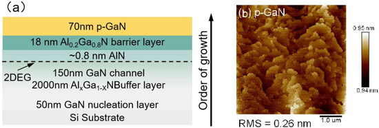
Figure 1.
(a) Cross-sectional schematic of epi-structure; (b) AFM image of p-GaN MOCVD growth.
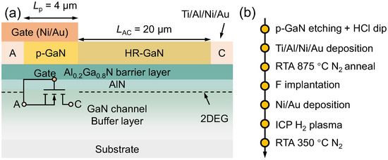
Figure 2.
(a) Cross-sectional schematic of the HPT-HAD; (b) fabrication process for the HPT-HAD.
2.2. Device Structure and Manufacturing Methods
Figure 2a illustrates the structure of the temperature sensor based on HPT-HAD. The p-GaN/AlGaN/AlN/GaN (70 nm/18 nm/~0.8 nm/~2 μm) epi-structure was grown on a 2-inch silicon substrate by metal-organic chemical vapor deposition, and the Mg-doping concentration of a p-GaN cap layer was about 4 × 1019 cm−3. The hybrid anode consists of the ohmic anode metal in contact with the two-dimensional electron gas (2DEG) and the p-GaN, and the gate metal connecting the p-GaN to the anode metal. Thus, the HPT-HAD is equivalent to a gate-to-source connected transistor.
The HPT-HAD was fabricated using traditional optical photolithography as shown in Figure 2b. It began with removing the p-GaN layer on the anode- and cathode-contact area by dry etching. Before the Ti/Al/Ni/Au metal stack deposition by electron beam evaporation, the sample was briefly dipped in diluted hydrochloric acid (HCl) to remove native surface oxides. The ohmic anode and cathode were formed after rapid thermal annealing (RTA) at 850 °C in N2 ambient. The device isolation was realized by fluorine implantation. The Ni/Au gate was evaporated on the p-GaN and ohmic anode. To form high-resistivity GaN (HR-GaN), the sample was load into the Oxford Plasmalab System 100 ICP 180 for H2 plasma treatments where the metal electrodes serve as hard masks, followed by thermal annealing by RTA at 623 K in N2 ambinet. The procedure of passivating H plasma is proficient in assuaging etching while transforming the processed GaN into a protective layer of high resistance. This modality engenders notable abatements in the deleterious impacts of etching, superficial state defects, and lattice fit defects, thereby amplifying the stability of devices and ameliorating the reverse leakage current. The treatment conditions were the same as the previous works [17,21]. Concomitantly, the Ni/Au metallic gate functions as a robust mask, preserving the p-type doping characteristics of the GaN beneath it from the H plasma processing. The minute segment of p-GaN that endures is able to exhaust the 2DEG below, adroitly regulating device turn-off. The reduced defects also mitigate the hot carrier effect at elevated temperatures, endowing our devices with improved thermal stability. The HPT-HADs had an p-GaN length (Lp) of 4 μm, an anode-to-cathode length (LAC) of 20 µm, and a width of p-GaN gate (WG) of 100 μm. No surface passivation was employed in the devices. The current-voltage (I–V) characteristics of the HPT-HAD temperature sensor were measured using Keysight B1500A semiconductor analyzer system and Janis Cryogenic Probe System from 73 to 573 K.
To validate the superior surface quality preservation achieved through H plasma as opposed to traditional ICP etching, we conducted separate H plasma and ICP etching procedures on a single p-GaN substrate. The stark contrast observed in Figure 3a,b provides compelling evidence that the H plasma treatment inflicts far less damage on the material surface compared to ICP etching.
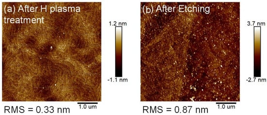
Figure 3.
AFM image of (a) after H plasma treatment, and (b) after ICP Etching.
3. Results
3.1. Performance and Principle
Figure 4a shows the temperature-dependent forward I–V characteristics of the HPT-HAD temperature sensor in a semi-log scale from 73 to 573 K. The HPT-HAD exhibited good rectifying behaviors at all measured temperatures. The current density of the device decreased as the temperature increased, which is due to the enhanced phonon scattering and thus reduced carrier mobility at high temperatures [22]. The OFF-state current density of the device was as low as 10 pA/mm, and the ION/IOFF ratio was 109~1011, which can be ascribed to the low surface damage by the etching-free plasma treatment technology. The HPT-HAD sensor showed a zero-temperature coefficient (ZTC) bias point of 1.6 V at which the device exhibited minimum temperature sensitivity, which is similar to reported devices [13,16].
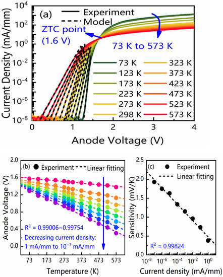
Figure 4.
(a) Forward I–V characteristics of the HPT-HAD temperature sensor in semi-log scale at different temperatures (73 to 573 K). (b) The forward anode voltage against with different fixed current density levels at all temperatures. (c)The sensitivity versus current density in semi-log scale.
Figure 4b presents the forward anode voltage (VA) across the HPT-HAD against temperature (T) at different fixed low current density (IA) levels. A highly linear relationship between the VA and T with a negative temperature coefficient from 73 to 573 K was observed, indicating that the HPT-HAD sensors can operate in a wide temperature range from cryogenic to high temperatures. This test is a step-by-step progression from the low temperature to the high temperature. The sensitivity (S) of the devices was defined as the temperature coefficient extracted from the linear fitting curves. Figure 4c depicts the device sensitivity at different current density levels. The device sensitivities at eight IA of 1, 10−1, 10−2, 10−3, 10−4, 10−5, 10−6, and 10−7 mA/mm were extracted as 0.38, 0.73, 0.96, 1.15, 1.34, 1.63, 1.75, and 1.93 mV/K, respectively. The relationship between the device sensitivity and the current density level can be expressed as follows: .
Based on the thermionic emission theory, the Schottky diode’s I–V relationship can be expressed as [23]
where A represents the Schottky junction’s area, A* is the effective Richardson constant, and the A* value for GaN is 26.3 A/(cm2∙K2) at 300 K. For AlGaN materials with Al compositions of 20%, the corresponding A value is 32.6 A/(cm2∙K2). Here, is the height of the Schottky barrier at zero bias, and IS represents the reverse saturation current.
When considering non-ideal effects such as image force, tunneling, recombination current of electron-hole pairs, hole injection effect, and series resistance, the IV equation can be expressed as [24,25]
In Equation (3), n represents the ideality factor, and RS is the equivalent series resistance of the current path. When V is greater than 3 kT/q, the equivalent series resistance RS is relatively small and can be simplified to
By taking the logarithm of both sides of Equations (3) and (4), we can obtain
The barrier height and ideality factor can be extracted from the slope and intercept of the lgI–V curve on a semi-logarithmic coordinate system, yielding:
Based on temperature-dependent testing results and the aforementioned calculation formula, we extracted the Schottky barrier and ideality factor of the device from 273 K to 523 K. As shown in Figure 5, the Schottky barrier of the device continues to rise while the ideality factor gradually approaches 1 as the temperature increases. This trend of the Schottky diode barrier and ideality factor variation with temperature is consistent with that reported in other articles [26].
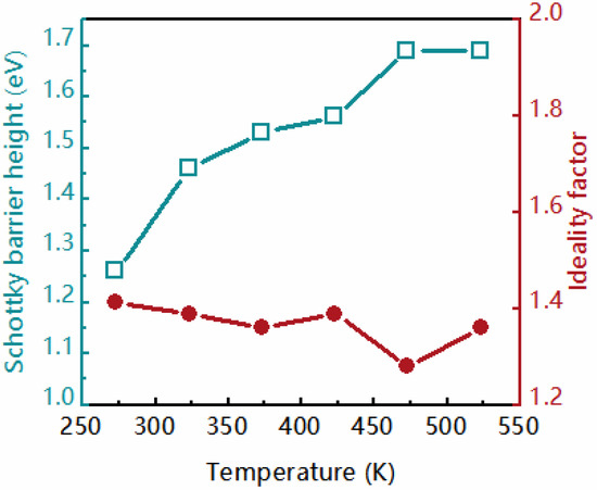
Figure 5.
The calculation results of the Schottky barrier and ideality factor of the device.
3.2. Reliability and Comparison
To evaluate the long-time reliability of the HPT-HAD temperature sensor, the device was measured under the anode current stress for a long time at high temperatures [27]. Figure 6 shows the changes in VA (ΔVA) at different temperatures for 1 h with the anode current density of 1 mA/mm. This suggests that the VA drifted negatively and more significantly with increasing temperature under the anode current stress and the highest ΔVA were only −1.60, −1.71, −2.87, and −2.89 mV at 298, 373, 473, and 573 K, respectively.
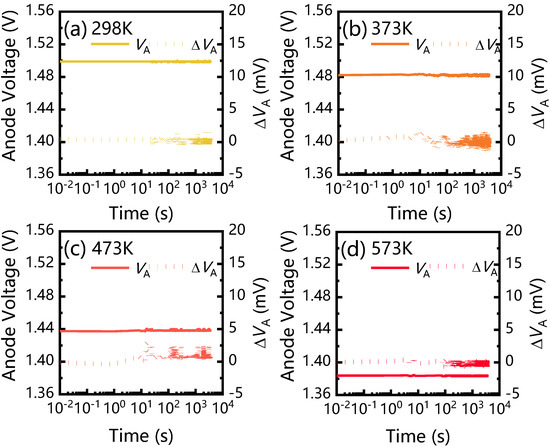
Figure 6.
Shift in Anode voltage during forward current densities of 1 mA/mm at (a) 298 K, (b)373 K, (c) 473 K, and (d) 573 K.
Figure 7 shows the ΔVA at different anode current stresses for 1000 s at 573, 298 and 73 K. At 573 K, the VA showed almost no change at high current density (10 μA/mm) and shifted negatively by about 120 mV at low current density (10 μA/mm). At 73 K, the device exhibited excellent long-term stability, with almost no performance drift observed. This may be because defects are frozen at 73 K, and the performance drift caused by carrier thermal effects cannot accumulate. At room temperature, this device also demonstrated impressive stability, which may be attributed to the reduction of defects. These results indicate the high reliability of the HPT-HAD temperature sensors.
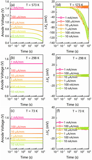
Figure 7.
Anode voltage over time measured during different forward current densities at (a) 573 K, (b) 298 K, (c) 73 K and shift in anode voltage measured during different forward current densities at (d) 573 K, (e) 298 K, (f) 73 K.
As shown in Figure 8, the performance of our device was benchmarked against some state-of-the-art temperature sensors based on AlGaN/GaN diodes [8,10,11,12,13,14,15,16,17]. Our HPT-HAD temperature sensor demonstrated sensitivity of 1.93 mV/K and a broad operating temperature range from 73 to 573 K. Moreover, the device showed remarkable stability at 73, 298, and 573 K. This desirable performance is mainly attributed to the H plasma treatment employed during the device fabrication process, which mitigates etching-induced damage and minimizes defects. Moreover, the H-treated p-GaN also serves to passivate and protect the device to some extent. Our previous work has confirmed the effectiveness of this approach [28].
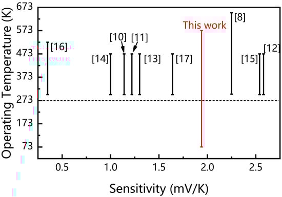
Figure 8.
Operating temperature vs. sensitivity for HPT-HAD temperature sensor compared with some reported state-of-the-art AlGaN/GaN diode temperature sensors.
4. Conclusions
In summary, we demonstrated a temperature sensor based on HPT-HAD that can operate from 73 to 573 K. The temperature sensor maintained a good linear relationship between forward anode voltage and temperature with a sensitivity of 1.93 mV/K. The experimental results were supported by an analytical model. Almost no forward anode voltage degradation during a long-time current stress test even at 573 K showed the high reliability of the HPT-HAD temperature sensors. These results indicate that the HPT-HAD is a promising candidate for temperature sensors in extreme environments.
Author Contributions
Conceptualization, A.Y. and B.Z.; methodology, A.Y.; software, X.W.; validation, W.S., Y.H. and T.C.; formal analysis, H.W.; investigation, J.Z.; resources, R.X.; data curation, X.Z.; writing—original draft preparation, A.Y.; writing—review and editing, G.Y.; visualization, Y.F.; supervision, Y.C.; project administration, Z.Z. All authors have read and agreed to the published version of the manuscript.
Funding
This work was supported in part by the National Key Research and Development Program of China (Grant No. 2021YFB3600202),the Fundamental Research Funds for the Central Universities (Grant No. WK5290000003), National Natural Science Foundation of China (Grant No. U1830112), Natural Science Foundation Key Project of Jiangxi Province, China (Grant No. 20202ACBL202001), Key Laboratory Construction Project of Nanchang (Grant No. 2020-NCZDSY-008), Jiangxi Province Double Thousand Plan (Grant No. S2019CQKJ2638). The authors would like to thank the Nano Fabrication Facility, the Platform for Characterization and Testing, Vacuum Interconnected Nanotech Workstation (NANO-X), and Suzhou Institute of Nano-Tech and Nano-Bionics, Chinese Academy of Sciences.
Conflicts of Interest
The authors declare no conflict of interest.
References
- Trung, T.Q.; Lee, N.-E. Flexible and Stretchable Physical Sensor Integrated Platforms for Wearable Human-Activity Monitoringand Personal Healthcare. Adv. Mater. 2016, 28, 4338–4372. [Google Scholar] [CrossRef]
- Blackburn, D. Temperature Measurements of Semiconductor Devices—A Review. In Proceedings of the 20th Annual IEEE Semiconductor Thermal Measurement and Management Symposium, San Jose, CA, USA, 9–11 March 2004; p. 70. [Google Scholar] [CrossRef]
- Udrea, F.; Santra, S.; Gardner, J.W. CMOS temperature sensors-Concepts, state-of-the-art and prospects. In Proceedings of the 31st International Semiconductor Conference, Sinaia, Romania, 13–15 October 2008; p. 31. [Google Scholar] [CrossRef]
- Kalker, S.; Ruppert, L.A.; van der Broeck, C.H.; Kuprat, J.; Andresen, M.; Polom, T.A.; Liserre, M.; De Doncker, R.W. Reviewing Thermal-Monitoring Techniques for Smart Power Modules. IEEE J. Emerg. Sel. Top. Power Electron. 2021, 10, 1326–1341. [Google Scholar] [CrossRef]
- Yang, F.; Pu, S.; Xu, C.; Akin, B. Turn-on Delay Based Real-Time Junction Temperature Measurement for SiC MOSFETs With Aging Compensation. IEEE Trans. Power Electron. 2020, 36, 1280–1294. [Google Scholar] [CrossRef]
- Chu, R. GaN power switches on the rise: Demonstrated benefits and unrealized potentials. Appl. Phys. Lett. 2020, 116, 090502. [Google Scholar] [CrossRef]
- Chen, K.J.; Haberlen, O.; Lidow, A.; Tsai, C.L.; Ueda, T.; Uemoto, Y.; Wu, Y. GaN-on-Si Power Technology: Devices and Applications. IEEE Trans. Electron Devices 2017, 64, 779–795. [Google Scholar] [CrossRef]
- Madhusoodhanan, S.; Sandoval, S.; Zhao, Y.; Ware, M.E.; Chen, Z. A Highly Linear Temperature Sensor Using GaN-on-SiC Heterojunction Diode for High Power Applications. IEEE Electron Device Lett. 2017, 38, 1105–1108. [Google Scholar] [CrossRef]
- Li, L.; Chen, J.; Gu, X.; Li, X.; Pu, T.; Ao, J.-P. Temperature sensor using thermally stable TiN anode GaN Schottky barrier diode for high power device application. Superlattices Microstruct. 2018, 123, 274–279. [Google Scholar] [CrossRef]
- Li, X.; Pu, T.; Li, L.; Ao, J.-P. Enhanced Sensitivity of GaN-Based Temperature Sensor by Using the Series Schottky Barrier Diode Structure. IEEE Electron Device Lett. 2020, 41, 601–604. [Google Scholar] [CrossRef]
- Li, X.; Pu, T.; Li, X.; Li, L.; Ao, J.-P. Correlation Between Anode Area and Sensitivity for the TiN/GaN Schottky Barrier Diode Temperature Sensor. IEEE Trans. Electron Devices 2020, 67, 1171–1175. [Google Scholar] [CrossRef]
- Li, X.; Pu, T.; Zhang, T.; Li, X.; Li, L.; Ao, J.-P. p-NiO/n-GaN Heterostructure Diode for Temperature Sensor Application. IEEE Sens. J. 2019, 20, 62–66. [Google Scholar] [CrossRef]
- Li, L.; Li, X.; Pu, T.; Cheng, S.; Li, H.; Ao, J.-P. Vertical GaN-Based Temperature Sensor by Using TiN Anode Schottky Barrier Diode. IEEE Sens. J. 2020, 21, 1273–1278. [Google Scholar] [CrossRef]
- Pu, T.; Li, X.; Wu, J.; Yang, J.; Lu, Y.; Liu, X.; Ao, J.-P. Recessed Anode AlGaN/GaN Schottky Barrier Diode for Temperature Sensor Application. IEEE Trans. Electron Devices 2021, 68, 5162–5166. [Google Scholar] [CrossRef]
- Li, L.; Pu, T.; Li, X.; Ao, J.-P. Effect of Anode Material on the Sensitivity of GaN Schottky Barrier Diode Temperature Sensor. IEEE Sens. J. 2021, 22, 1933–1938. [Google Scholar] [CrossRef]
- Kwan, A.M.H.; Guan, Y.; Liu, X.; Chen, K.J. A Highly Linear Integrated Temperature Sensor on a GaN Smart Power IC Platform. IEEE Trans. Electron Devices 2014, 61, 2970–2976. [Google Scholar] [CrossRef]
- Wei, X.; Zhang, X.; Zhou, X.; Ma, Y.; Tang, W.; Chen, T.; Liu, W.; Tang, W.; Yu, G.; Fan, Y.; et al. Dual Current and Voltage Sensitivity Temperature Sensor Based on Lateral p-GaN/AlGaN/GaN Hybrid Anode Diode. IEEE Sens. J. 2021, 21, 22459–22463. [Google Scholar] [CrossRef]
- Rajashekara, K.; Akin, B. A review of cryogenic power electronics—Status and applications. In Proceedings of the IEEE International Electric Machines and Drives Conference (IEMDC), Chicago, IL, USA, 12–15 May 2013; pp. 899–904. [Google Scholar] [CrossRef]
- Gui, H.; Chen, R.; Niu, J.; Zhang, Z.; Tolbert, L.M.; Wang, F.F.; Blalock, B.J.; Costinett, D.; Choi, B.B. Review of Power Electronics Components at Cryogenic Temperatures. IEEE Trans. Power Electron. 2019, 35, 5144–5156. [Google Scholar] [CrossRef]
- Nela, L.; Perera, N.; Erine, C.; Matioli, E. Performance of GaN Power Devices for Cryogenic Applications Down to 4.2 K. IEEE Trans. Power Electron. 2020, 36, 7412–7416. [Google Scholar] [CrossRef]
- Wei, X.; Shen, W.; Zhou, X.; Tang, W.; Ma, Y.; Chen, T.; Wang, D.; Fu, H.; Zhang, X.; Lin, W.; et al. 2.69 kV/2.11 mΩ∙cm2 and Low Leakage p-GaN Stripe Array Gated Hybrid Anode Diodes with Low Turn-on Voltage. IEEE Electron Device Lett. 2022, 44, 13–16. [Google Scholar] [CrossRef]
- Fu, H.; Fu, K.; Liu, H.; Alugubelli, S.R.; Huang, X.; Chen, H.; Montes, J.; Yang, T.-H.; Yang, C.; Zhou, J.; et al. Implantation-and etching-free high voltage vertical GaN p–n diodes terminated by plasma-hydrogenated p-GaN: Revealing the role of thermal annealing. Appl. Phys. Express 2019, 12, 051015. [Google Scholar] [CrossRef]
- Mansoor, M.; Haneef, I.; Akhtar, S.; De Luca, A.; Udrea, F. Silicon diode temperature sensors—A review of applications. Sens. Actuators A Phys. 2015, 232, 63–74. [Google Scholar] [CrossRef]
- Zhang, N.; Lin, C.-M.; Senesky, D.G.; Pisano, A.P. Temperature sensor based on 4H-silicon carbide pn diode operational from 20 °C to 600 °C. Appl. Phys. Lett. 2014, 104, 073504. [Google Scholar] [CrossRef]
- Schmitz, A.C.; Ping, A.T.; Khan, M.A.; Chen, Q.; Yang, J.W.; Adesida, I. Schottky barrier properties of various metals on n-type GaN. Semicond. Sci. Technol. 1996, 11, 1464–1467. [Google Scholar] [CrossRef]
- Bian, Z.; Su, K.; Zhang, J.; Zhao, S.; Zhou, H.; Zhang, W.; Zhang, Y.; Zhang, T.; Chen, J.; Dang, K.; et al. Gamma irradiation impact on GaN quasi-vertical Schottky barrier diodes. J. Phys. D Appl. Phys. 2019, 53, 045103. [Google Scholar] [CrossRef]
- De Luca, A.; Pathirana, V.; Ali, S.Z.; Udrea, F. Silicon on insulator thermodiode with extremely wide working temperature range. In Proceedings of the 2013 Transducers & Eurosensors XXVII: 17th International Conference on Solid-State Sensors, Actuators and Microsystems (Transducers & Eurosensors XXVII), Barcelona, Spain, 16–20 June 2013; p. 1911. [Google Scholar] [CrossRef]
- Wei, X.; Zhang, X.; Tang, W.; Liu, W.; Zhou, X.; Tang, W.; Ma, Y.; Chen, T.; Huang, X.; Qian, H.; et al. 2.0 kV/2.1 mΩ·cm2 Lateral p-GaN/AlGaN/GaN Hybrid Anode Diodes with Hydrogen Plasma Treatment. IEEE Electron Device Lett. 2022, 43, 693–696. [Google Scholar] [CrossRef]


Disclaimer/Publisher’s Note: The statements, opinions and data contained in all publications are solely those of the individual author(s) and contributor(s) and not of MDPI and/or the editor(s). MDPI and/or the editor(s) disclaim responsibility for any injury to people or property resulting from any ideas, methods, instructions or products referred to in the content. |
© 2023 by the authors. Licensee MDPI, Basel, Switzerland. This article is an open access article distributed under the terms and conditions of the Creative Commons Attribution (CC BY) license (https://creativecommons.org/licenses/by/4.0/).