Article

Effect of Annealing on the Structure of Composite Passivation Films Prepared by Magnetron Sputtering Deposition on the Surface of HgCdTe

1
Kunming Institute of Physics, No. 31, Jiaochang East Road, Kunming 650221, China
2
Faculty of Material Science and Engineering, Kunming University of Science and Technology, Kunming 650093, China
3
Research Center for Analysis and Measurement, Kunming University of Science and Technology, Kunming 650093, China
*
Authors to whom correspondence should be addressed.
Crystals 2022, 12(7), 983; https://doi.org/10.3390/cryst12070983
Submission received: 14 June 2022 / Revised: 10 July 2022 / Accepted: 13 July 2022 / Published: 15 July 2022

Abstract

:
In this study, the structural evolution of the CdTe/ZnS composite passivation films on the surface of infrared HgCdTe material before and after annealing was comparatively explored. The surface morphology and microstructure of the passive films before and after annealing were characterized by scanning electron microscope, X-ray diffraction, atomic force microscopy, and Raman and X-ray photoelectron spectroscopy to determine the effects of the annealing process on the surface crystal defects of the films. The results show that annealing at 320 °C for three hours can improve crystal quality, ameliorate the surface density, and reduce the dislocation density of grains, while the Hg grains inhibited by tellurium-rich growth during the annealing process return to the normal growth state, and the S signal can be detected near the surface after annealing. This finding indicates that high-temperature annealing promotes the inhibited grain growth and also causes diffusion of surface elements, thus smoothing the compositional gradient at the passivation interface of the films.

1. Introduction

Within the last decade, the transformation to production-based technology will be completed for ultra–large–scale, dual-color, very long wave, weak signal, and high–temperature working infrared focal plane technology; HgCdTe is the most commonly used material for the development of infrared focal plane devices [1,2]. HgTe is a mixture of HgTe with negative forbidden band and positive forbidden band CdTe, making it an (HgTe)1-x(CdTe)x binary material with a direct band gap, and its forbidden band width can be continuously adjusted in the range of 0 to 1.6 eV with the variation of x. It can be used to realize detection of the whole infrared band and is the most important infrared detector material at present [3,4]. In order to better combat the current COVID–19 epidemic, the demand for thermometers has increased greatly, and non-contact infrared thermometers can calculate the surface temperature of an object by measuring the intensity of infrared radiation emitted by the target, avoiding contact with the object throughout, which is more convenient and efficient. Moreover, thermal imaging cameras can produce thermal image images based on the infrared radiation emitted from the scene, thus playing an important role in geological disaster protection such as ground disaster notification, rock fall detection, and inspection of landslides and collapses.
The surface passivation process has affected device performance in the preparation of HgCdTe infrared devices. A good passivation layer can reduce damage to the device surface, decrease the device surface interface state, reduce the device surface leakage current, abate the device surface composite speed and 1/f noise, and improve the detector dynamic resistance and reverse its breakdown voltage to improve the detector chip performance, thus increasing the yield [5,6,7]. Much research has been performed to improve the quality of passivation films, and one of the most widely used methods is annealing. According to previous studies [8,9,10,11], Haakenaasen et al. found that annealing can smooth the compositional gradient at the film––passivation interface and can create a specified concentration of vacancies in the material; X. Wang et al. investigated the capacitance–voltage characteristics of metal–insulator semiconductor structures based on Hg1–xCdxTe (x = 0.218) with CdTe passivation before and after the passivation annealing process. They concluded that the annealing process propagates an equivalent electrical surface for CdTe/HgCdTe uniformly from the principal physical interface to the inside of the bulk material, thereby improving the characteristics of the CdTe passivation layer. Currently, CdTe/ZnS composite passivation films are widely used due to their better passivation effect and reliability and are the mainstream choice of film system for CdTe surface passivation today [12].
In this work, analytical techniques such as scanning electron microscopy, X-ray diffraction, atomic force microscopy, and Raman and X-ray photoelectron spectroscopy were adopted to study the structure of the CdTe/ZnS composite passivation films on the CdTe surface. The changes in the surface crystal structure, flatness, and element distribution before and after annealing were compared and analyzed to summarize the structural evolution of the passivation film surface before and after annealing.

2. Materials and Methods

The material preparation process is shown in Figure 1. The sample size is 20 mm × 25 mm, and the HgCdTe (MCT) film is grown on a 1 mm thickness CdZnTe (CZT) substrate with a thickness of 10 μm, and then the CdTe/ZnS composite passivation film layer is prepared on the HgCdTe film using RF magnetron, where the thickness of both CdTe and ZnS passivation films is 360 nm. The formed heterostructured film material is then subjected to 320 °C/3 h, nitrogen–protected annealing atmosphere.
The morphological characteristics of the film surface were analyzed using a high-resolution field emission scanning electron microscope (Nova NanoSEM450, FEI, Hillsboro, OR, USA) and an atomic force microscope (Dimension Icon, Bruker, Germany) with a resolution of 1.5 nm (10 Kv) in low vacuum mode for SEM, 0.1 A for AFM, and an operating voltage of 220 V; using an X-ray diffractometer (Empyrean, Malvern, The Netherlands), a laser confocal Raman spectrometer (LabRAM HR/HORIBA Jobin Yvon S.A.S.) and X-ray photoelectron spectrometer (Kalpha, ThermoFisher, Oxford, United Kingdom) were used to analyze the microstructure of the surface of the compliant passivated films, where the XRD radiation source was monochromatic Cu Kα (λ = 1.54056) with an operating voltage and current of 40 kV and 40 mA, respectively, a Raman spectrometer with a focal length of 800 mm and a resolution of 2 μm, and an XPS radiation source of Al Kα (energy 1486.6 eV at 10−7 Pa pressure) with a scan step of 0.05 eV/step.

3. Results and Discussion

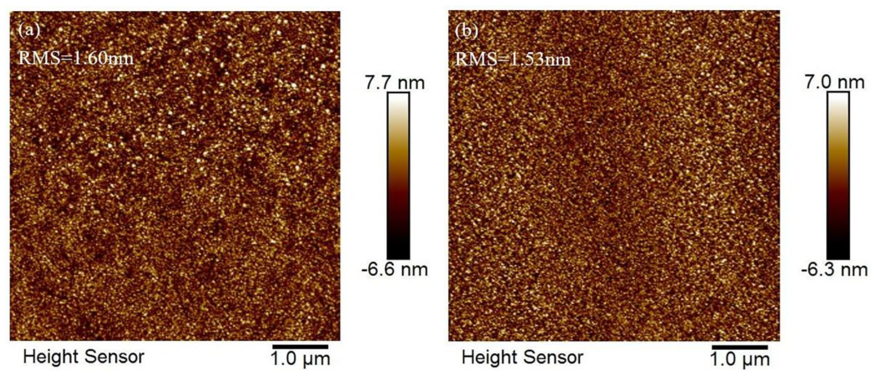
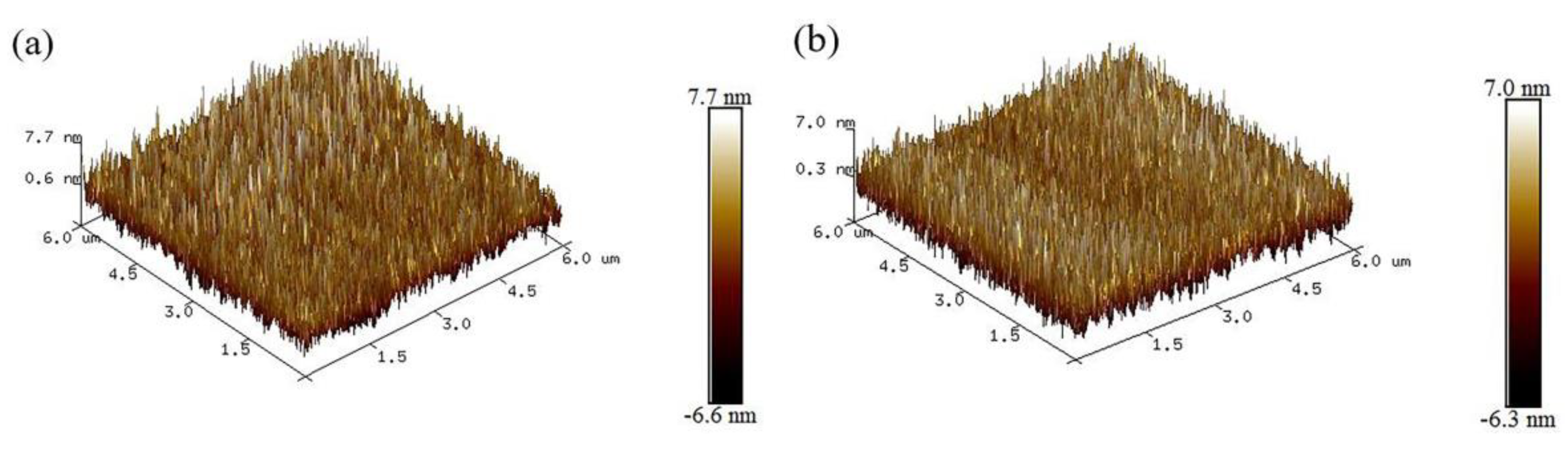
3.1. Surface Morphological Features

Figure 2a,b shows the SEM images of the surface of the heterogeneous film before and after annealing. The surface film distribution shown in Figure 2a has fine cracks and the film denseness is poor. Compared with before annealing, Figure 2b presents the dense surface of the sample after annealing with a more uniform particle distribution. When the ZnS passivation film was prepared by RF magnetron, the Zn particles and S particles failed to obtain enough energy to migrate to the proper position [13], and taking high–temperature annealing can re–energize the Zn particles and S particles within the film to migrate the atoms within the film to the proper position, which improves the meritocratic orientation of the crystal and releases the stress due to lattice mismatch or distortion to a certain extent, thus improving the film formation quality [14], and high–temperature annealing can improve the crystallinity of the crystals.
Figure 3 shows the two-dimensional AFM images of the passivated film surface before and after annealing. The surface roughness of the sample before and after annealing is less than 2 nm, which indicates that the surface of the passivated film is smooth before and after annealing. Figure 4a,b shows the 3D AFM images of the surface of the passivated film before and after annealing. The surface size undulation of the sample before annealing is about 14.3 nm and after annealing is about 13.3 nm, which indicates that the surface of the film is flatter after annealing. It can be seen from Figure 3a that before annealing, the particles on the surface of the film were irregularly arranged and poorly dense; after annealing, as shown in Figure 3b and Figure 4b, the film became flat and dense, and the uniformity was significantly improved.
The reason for the significant changes in the surface morphology of the films is mainly due to the fact that, on the one hand, the crystallinity of the particles in the films is improved during the annealing process, which makes the films shrink denser and flat; on the other hand, the annealing treatment of the films releases the surface stresses, which helps the sub-stable particles to be able to recrystallize [15]. This shows that annealing is an effective means to improve the quality of films.

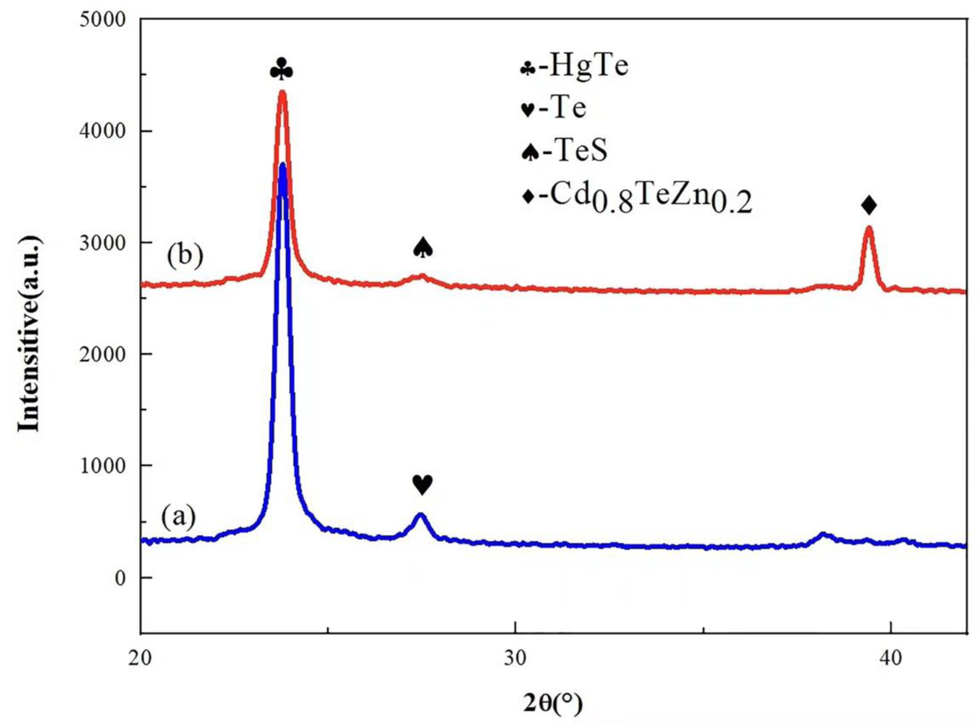
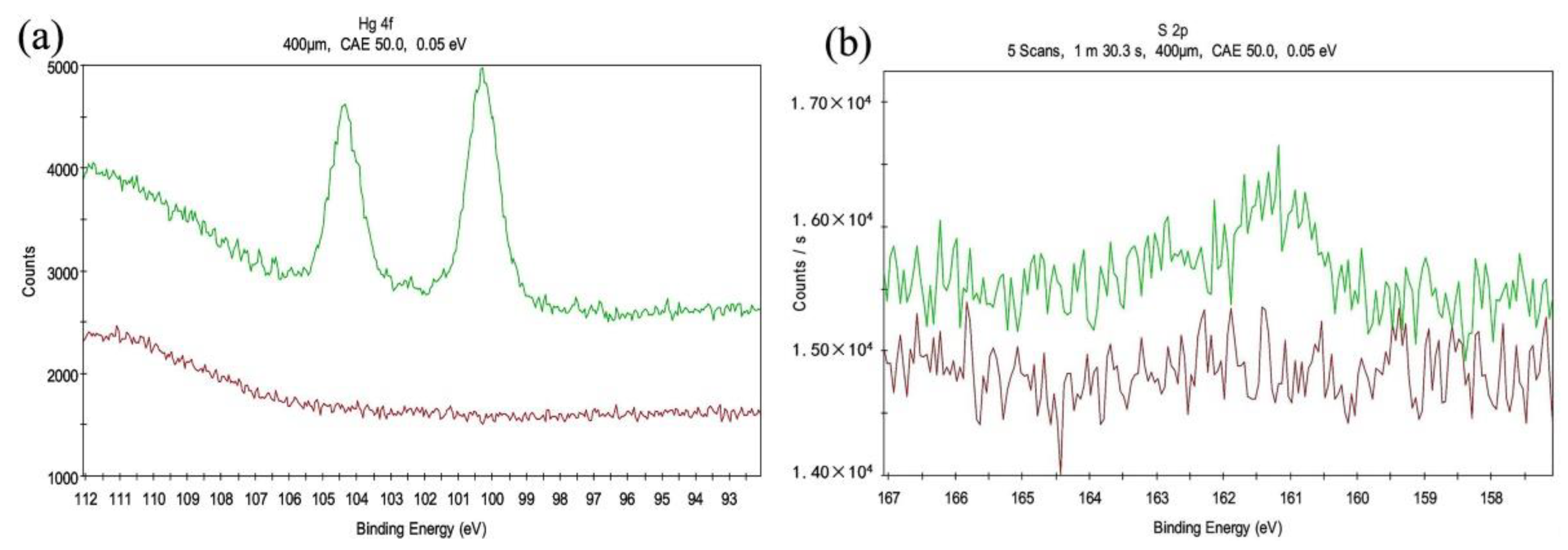
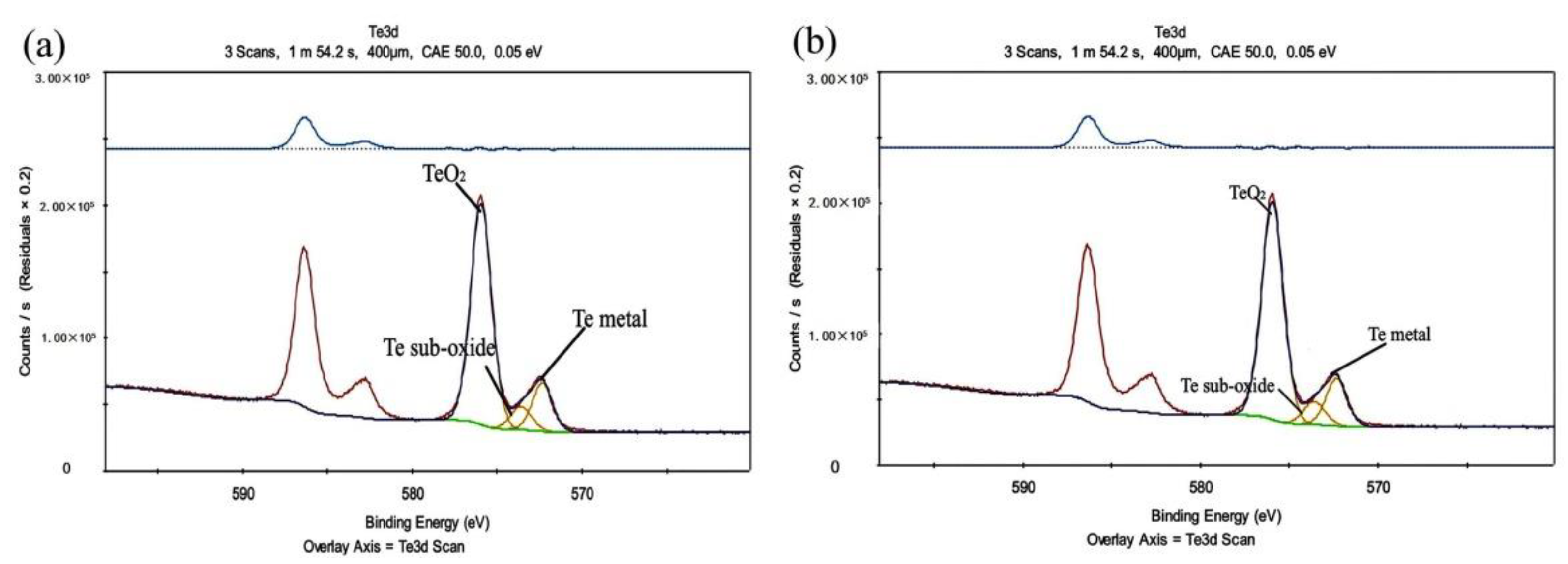
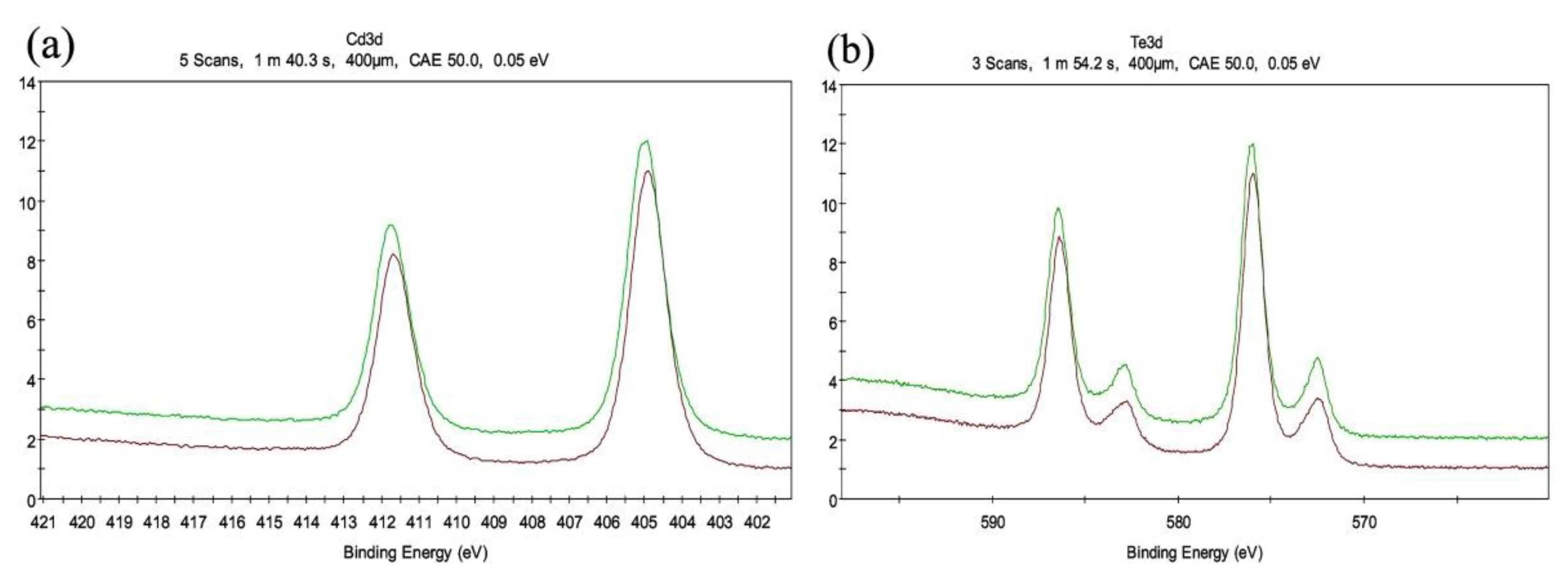
3.2. Structural Analysis of Composite Passivation Films

The XRD spectra of the surfaces of the heterogeneous structured films before and after annealing are shown in Figure 5. Comparing Figure 5a,b, HgTe grains are present both before and after annealing, but after annealing the Te disappears, and a small amount of TeS and a large amount of CdTeZn grains are generated. Grain size (D) and dislocation density (ρ) are determined by the following two equations:
  D = 0.9 λ β cos θ
  ρ = 3 2 π ε 2 1 2 Db
From the above equation, the grain size of HgTe before annealing is 0.2839 nm and the dislocation density is 34.2784 nm−2, and the grain size of HgTe after annealing is 0.3060 nm and the dislocation density is 29.5077 nm−2. The grain size of HgTe increases and the dislocation density decreases after annealing, and the HgTe defects are partially eliminated during the annealing process. Moreover, the FWHM of HgTe before and after annealing is 0.499 nm and 0.463 nm, respectively, and the crystal quality is improved after annealing.
The Cd0.8TeZn0.2 tissue appears after annealing, and the defect is analyzed; because the edges of the CdZnTe substrate are loose, the particles at the edges of the CdZnTe substrate are easily dislodged during the processing of the substrate before growth, and some of the particles will adhere to the surface of the substrate. During the growth epitaxy process, the attached particles are encapsulated by the growth melt to form a raised spot. Since this particle is a small single crystal, an epitaxial process also occurs on its crystalline surface [16]; during the annealing process the single crystal grows, so the Cd0.8TeZn0.2 absorption peak increases and the content increases after annealing.
The liquid–phase epitaxial growth environment is in a Te–rich state, the sample surface is Te rich, and there are some regions with 100% Te defects in the components [17]; after annealing, some of the defects in these regions are eliminated owing to the re–melting effect of the mother liquor, and some of them are combined with S particles to form TeS.
The Raman spectra before and after annealing largely overlap, but in the specific data, as shown in the inset to Figure 6, a significant strong peak is found at a Raman shift of 132.774 cm−1, and the Raman peaks after annealing are smaller than those of the unannealed specimens. As can be judged from the above, the intensity of the defect pattern decreases after annealing, indicating an improvement in surface finish compared to the unannealed state; however, from the overall macroscopic point of view, the characteristic peaks do not show significant broadening and shifting, implying that the degree of component partitioning between the solid and liquid phases during the annealing process is small [18].
As shown in Table 1 and Table 2, the content of Hg on the surface of the passive film is 0.12% before annealing and 3.10% after annealing. The atomic weight of Hg on the surface is increased by 210% after annealing compared with that before annealing, and the S signal could be detected on the surface of the sample after annealing. Figure 7a,b also demonstrate that Hg and S signals were detected on the surface of the sample after annealing, with a binding energy of 100.3 eV for Hg 4f7/2 and 161.5 eV for S 2p3/2 (corresponding to metal sulfides). The XRD analysis shows that the metal sulfide fraction corresponding to the surface of the film is TeS.
These data show that the content of Hg near the surface increases significantly after annealing because this experiment is undertaken under tellurium-rich conditions, the Hg/Te beam is relatively low, so most of the defects formed on the surface during the growth process involve a significant lack of mercury. However, it is not the absence of Hg, but the preferential growth of Te in the surface under these experimental conditions nucleates to form crystals and the growth of these crystals is disordered, and this disordered nucleation growth of crystalline surfaces further hinders the normal growth of Hg [19]. During the annealing process, Hg gradually returns to its normal growth state, and thus an increase in near–surface Hg content will be detected.
As shown in Figure 8, XPS patterns before and after annealing, Te is bimodal before and after annealing, where the peak at 572 eV represents metallic Te and that at 576 eV denotes Te4+. After annealing, the TeO2 peak weakens, indicating that part of Te4+ is reduced during the annealing process. From the split–peak fitted images of Te elements (Figure 9), there are sub–oxidized particles of Te on the surface of the films before and after annealing: combined with data in Table 3 and Table 4, it can be seen that not only Te4+, but also some sub–oxidized inclusions of Te are reduced during the annealing process. The quantitative regression showed that the metal Te content increased from 16.02% to 18.73% before and after annealing.
As shown in Figure 10, the XPS scan step is 0.05 eV per step, and the comparison after correction with C1s = 284.8 eV indicates that the binding energy is shifted by 0.1 eV towards the high–energy end for both Cd and Te after annealing.

4. Conclusions

(1) The annealing treatment releases the stress on the surface of the passive film to a certain extent, improving the crystallinity of the crystals on the surface of the film, making the surface of the passive film more dense, flat, and uniform, thus improving the quality of the film and resulting in a more ideal surface morphology of the passive film.
(2) After high-temperature annealing, the grain size of the film surface increases and the dislocation density decreases, while some of the defects caused by the tellurium–rich liquid–phase epitaxial growth are eliminated due to the re–melting effect of the mother liquor, but the degree of solid–liquid–phase component partitioning is not significant.
(3) Significant signals of Hg and S can be detected near the surface after annealing, indicating that high–temperature annealing causes diffusion of surface elements and promotes the growth of suppressed grains, smoothing the composition gradient at the interface of passivation films, thus optimizing the surface structure of the composite passivation films.

Author Contributions

Conceptualization, J.J. and Y.H.; methodology, X.W. (Xiangqian Wang) and J.C.; validation, X.W. (Xiao Wang) and P.Z.; investigation, L.L. and S.Y.; data curation, Q.Q.; writing—original draft preparation, Y.L.; writing—review and editing, Y.L. All authors have read and agreed to the published version of the manuscript.

Funding

Yunnan Provincial Science and technology project grant number 202104AR040008; Science and Technology Innovation Base Construction Project Fund grant number 202207AB110003; Key Research and Development Project of Yunnan Province and International Science and Technology Cooperation Project grant number 202103AF140004; Applied Basic Research project of Yunnan Province grant number 202101AT070123 and Ten Thousand Talent Program of Yunnan Province grant number YNWR-QNBJ-2019-106.

Institutional Review Board Statement

Not applicable.

Informed Consent Statement

Not applicable.

Data Availability Statement

All data are fully available without restriction. The datasets used and/or analyzed during the current study are available from the corresponding author on reasonable request.

Conflicts of Interest

The authors declare no conflict of interest.

References

  1. Lei, W.; Antoszewski, J.; Faraone, L. Progress, challenges, and opportunities for HgCdTe infrared materials and detectors. Appl. Phys. Rev. 2015, 2, 041303. [Google Scholar] [CrossRef]
  2. Rogalski, A. Progress in focal plane array technologies. Prog. Quantum Electron. 2012, 36, 342–473. [Google Scholar] [CrossRef]
  3. Wang, H.; Hong, J.; Yue, F.G.; Jing, C.B.; Chu, J.H. Optical homogeneity analysis of Hg1–xCdxTe epitaxial layers: How to circumvent the influence of impurity absorption bands. Infrared Phys. Technol. 2017, 82, 1–7. [Google Scholar] [CrossRef]
  4. Sun, C.H.; Zhang, P.T.; Zhang, N.; Chen, X.; Chen, Y.Y.; Ye, Z.H. ZnS thin films grown by atomic layer deposition on GaAs and HgCdTe substrates at very low temperature. Infrared Phys. Technol. 2017, 85, 280–286. [Google Scholar] [CrossRef]
  5. Li, X.J.; Han, F.Z.; Li, D.S.; Li, L.H.; Hu, Y.B.; Kong, J.C.; Zhao, J.; Zhu, Y.F.; Zhuang, J.S.; Gi, R.B. Variable-area diodes with LW HgCdTe. J. Infrared Millim. Waves 2016, 35, 412–417. [Google Scholar]
  6. Sheng, F.F.; Zhou, C.H.; Sun, S.W.; Yang, J.R. Influences of Te-Rich and Cd-Rich precipitates of CdZnTe substrates on the surface defects of HgCdTe liquid-phase epitaxy materials. J. Electron. Mater. 2014, 43, 1397–1402. [Google Scholar] [CrossRef]
  7. Li, Q.; He, J.L.; Hu, W.D.; Chen, L.; Chen, X.S.; Lu, W. Influencing Sources for Dark Current Transport and Avalanche Mechanisms in Planar and Mesa HgCdTe p-i-n Electron-Avalanche Photodiodes. IEEE Trans. Electron Devices 2018, 865, 572–576. [Google Scholar] [CrossRef]
  8. Wang, X.; Zhou, S.M.; Sun, C.H.; Wei, Y.F.; Shen, H.; Lin, C. Annealing of au doped HgCdTe covered by electron beam evaporated CdTe. J. Infrared Millim. Waves 2018, 37, 399–402. [Google Scholar]
  9. Haakenaasen, R.; Selvig, E.; Heier, A.C.; Lorentzen, T.; Trosdahl-Iversen, L. Improved passivation effect due to controlled smoothing of the CdTe-HgCdTe interface gradient by thermal annealing. J. Electron. Mater. 2019, 48, 6099–6107. [Google Scholar] [CrossRef]
  10. Wang, X.; He, K.; Chen, X.; Li, Y.; Lin, C.; Zhang, Q.Y.; Ye, Z.H.; Xin, L.W.; Gao, G.L.; Yan, X.; et al. Effect of annealing on the electrophysical properties of CdTe/HgCdTe passivation interface by the capacitance–voltage characteristics of the metal—Insulator-semiconductor structures. AIP Adv. 2020, 10, 105102. [Google Scholar] [CrossRef]
  11. Lu, Q.; Wang, X.; Wei, Y.F.; Sun, Q.Z.; Lin, C. Investigation of the influence of graded-gap layer formed by annealing on the electrical properties of the near-surface of LPE HgCdTe using MIS structure. Mater. Res. Express 2021, 8, 015903. [Google Scholar] [CrossRef]
  12. White, J.K.; Antoszewski, J.; Pal, R.; Musca, C.A.; Dell, J.M.; Faraone, L.; Piotrowski, J. Passivation Effects on Reactive Ion Etch Formed n-on-p Junctions In HgCdTe. J. Electron. Mater. 2002, 31, 743–748. [Google Scholar] [CrossRef]
  13. Subrina, R.; Han, L.; Neal, A.T.; Shin, M.; John, B.; Zhao, H.P. Towards High-Mobility Heteroepitaxial β-Ga2O3 on Sapphire—Dependence on The Substrate Off-Axis Angle. Phys. Status Solidi A 2018, 215, 1700467. [Google Scholar]
  14. Wang, Y.; Pu, T.F.; Li, X.B.; Li, L.A.; Ao, J.P. Application of p-type NiO deposited by magnetron reactive sputtering on GaN vertical diodes. Mater. Sci. Semicond. Process. 2021, 125, 105628. [Google Scholar] [CrossRef]
  15. Zhang, X.L.; Li, Z.Z.; Fan, J.J. An effect of rapid post-annealing temperature on the properties of cupric oxide thin films deposited by a remote plasma sputtering technique. Mater. Sci. Semicond. Process. 2022, 137, 106227. [Google Scholar] [CrossRef]
  16. Wei, Y.F.; Xu, Q.Q.; Chen, X.J.; Zhang, C.J.; Sun, S.W.; Fang, W.Z.; Yang, J.R. Control of surface defects in HgCdTe film grown by liquid phase epitaxy. J. Infrared Millim. Waves 2009, 28, 246–248. [Google Scholar] [CrossRef]
  17. Zhang, Y.; Wu, J.; Mu, S.; Zuo, D.F.; Li, D.S. Surface defects of Liquid Phase Epitaxial growth of HgCdTe film induced by Te-rich precipitates in CdZnTe substrates. J. Infrared Millim. Waves 2018, 37, 728–733. [Google Scholar]
  18. Yu, W.; He, J.; Sun, Y.T.; Zhu, H.F.; Han, L.; Fu, G.S. Raman Spectra of Nano-SiC Thin Film Prepared by Plllse Laser Crystallization. Chin. J. Iasers 2004, 31, 513–515. [Google Scholar]
  19. Aoki, T.; Chang, Y.; Badano, G.; Zhao, J.; Grein, C.; Sivananthan, S.; David, J.S. Electron Microscopy of Surface-Crater Defects on HgCdTe/CdZnTe(211)B Epilayers Grown by Molecular-Beam Epitaxy. J. Electron. Mater. 2003, 32, 703–709. [Google Scholar] [CrossRef]
Figure 1. (a) Structure of the three-layer heterogeneous films with prepared CdTe passivation films; (b) schematic diagram of the process of ZnS passivation films prepared by RF magnetron; (c) annealing process of the four-layer heterogeneous films.
Crystals 12 00983 g001
Figure 2. SEM images of the surface of heterogeneous films: (a) without annealing and (b) after annealing.
Crystals 12 00983 g002
Figure 3. AFM 2-d scan images of heterogeneous films: (a) without annealing; (b) after annealing.
Crystals 12 00983 g003
Figure 4. AFM 3D scan image of heterogeneous films: (a) without annealing and (b) after annealing.
Crystals 12 00983 g004
Figure 5. XRD spectra of heterogeneous films before and after annealing: (a) without annealing and (b) after annealing.
Crystals 12 00983 g005
Figure 6. Raman spectra of heterogeneous films before and after annealing. (Inset) Raman spectra of the region near the Raman shift of 132.774 cm−1 magnified.
Crystals 12 00983 g006
Figure 7. XPS patterns of Hg and S elements before (red) and after (green) annealing of the passive film surface: (a) Hg4f and (b) S2p.
Crystals 12 00983 g007
Figure 8. XPS pattern of Te elements before (red) and after (green) annealing of the passive film surface.
Crystals 12 00983 g008
Figure 9. Fractional peak fit images of Te elements on the surface before and after annealing: (a) without annealing and (b) after annealing.
Crystals 12 00983 g009
Figure 10. Images of Cd3d and Te3d core energy level shifts before (red) and after (green) annealing after correction: (a) Cd3d and (b) Te3d.
Crystals 12 00983 g010
Table 1. Elemental identification and quantification before annealing.
NameStart BEPeak BEEnd BEHeight CPSFWHM eVArea (P) CPS.eVAtomic %Q
Cd3d421.03404.90401.13104,645.231.12231,266.5532.861
Te3d598.03575.96560.13170,974.041.36604,372.7067.021
Hg4f105.98101.2698.18597.210.00768.100.121
Table 2. Elemental identification and quantification after annealing.
NameStart BEPeak BEEnd BEHeight CPSFWHM eVArea (P) CPS.eVAtomic %Q
Hg4f107.08100.2796.588738.661.0418,417.983.101
S2p164.53161.39158.63887.550.691903.533.731
Cd3d421.03404.98401.13103,100.641.13226,192.0433.621
Te3d598.03576.04560.13144,604.551.35513,247.9859.541
Table 3. Te elemental identification and quantification before annealing.
NameStart BEPeak BEEnd BEHeight CPSFWHM eVArea (P) CPS.eVAtomic %Q
Te metal598.03572.34560.1336,497.421.3854,862.1716.021
Te sub–oxide598.03573.60560.1317,660.141.4427,553.868.051
TeO2598.03575.94560.13166,164.481.44259,254.5675.931
Table 4. Te elemental identification and quantification after annealing.
NameStart BEPeak BEEnd BEHeight CPSFWHM eVArea (P) CPS.eVAtomic %Q
Te metal598.03572.49560.1336,104.671.3854,386.6418.731
Te sub–oxide598.03573.79560.1311,222.341.4517,524.556.041
TeO2598.03576.03560.13139,482.671.45217,812.9275.231
Publisher’s Note: MDPI stays neutral with regard to jurisdictional claims in published maps and institutional affiliations.

