Article

The Influence of Argon Plasma on Organic Perovskite MAPbI3 Film Doped with Inorganic Perovskite CsPbI3 Quantum Dots (QDs)

1
Department of Opto-Electronic and Communication Engineering, Xiamen University of Technology, Xiamen 361024, China
2
Department of Materials Science and Engineering, Da-Yeh University, Changhua 51591, Taiwan
3
Fujian Key Laboratory of Optoelectronic Technology and Devices, Xiamen University of Technology, Xiamen 361024, China
4
Department of Applied Physics, National University of Kaohsiung, Kaohsiung University Rd., Kaohsiung 81148, Taiwan
5
Department of Electronic Engineering, National Formosa University, Wenhua Rd., Yunlin 632301, Taiwan
6
Department of Mechatronic Engineering, National Taiwan Normal University, Heping East Rd., Taipei 10610, Taiwan
7
Department of Electrical Engineering, Kao Yuan University, Zhongshan Rd., Kaohsiung 82151, Taiwan
8
Department of Electronic Engineering, Center for Environmental Toxin and Emerging–Contaminant Research, Super Micro Mass Research & Technology Center, Cheng Shiu University, Chengcing Rd., Kaohsiung 82146, Taiwan
*
Authors to whom correspondence should be addressed.
Crystals 2022, 12(6), 799; https://doi.org/10.3390/cryst12060799
Submission received: 22 April 2022 / Revised: 21 May 2022 / Accepted: 27 May 2022 / Published: 6 June 2022
(This article belongs to the Special Issue Solution-Based Processes in Semiconductors and Electronic Devices)

Abstract

:
In this study, the inorganic perovskite cesium lead triiodide (CsPbI3) quantum dots (QDs) produced by hot-injection method were added into the hybrid perovskite methylamine lead triiodide (CH3NH3PbI3; MAPbI3) to form composite perovskite film. It is not easy for argon (Ar) to react with perovskite. Therefore, argon plasma was used to optimize the properties of the surface. However, methylamine lead triiodide molecular will be degraded by excessive wattage. Therefore, the influence of plasma power acting on composite perovskite film was investigated. The experimental results show that the light absorption capacity can be increased by argon plasma power of 140 watt (W) acting on the surface of films because organic impurities are removed and surface morphology of film is changed.

1. Introduction

To find the main source of clean and sustainable energy on the earth, researchers have long sought to convert solar into electricity through the photovoltaic effect of light-absorbing semiconductors. As the absorber layer material of solar cells, monocrystalline silicon, polycrystalline silicon, and amorphous silicon have attracted much attention due to their high efficiency and stability. However, there are some disadvantages for silicon, such as high-temperature process and vacuum process. Based on the above statements, perovskite methylamine lead triiodide (CH3NH3PbI3; MAPbI3) has been greatly studied due to its excellent power conversion efficiency, high quantum yield, low-cost manufacturing, and significant absorbance performance [1,2,3]. Needless to say, it has been widely used in solar cells, light-emitting diodes (LED), and photodetectors [4]. Nevertheless, MAPbI3 is easily degraded into PbI2 under long-term exposure to moisture, heat, and air, and it will affect the efficiency of the perovskite solar cell [5,6]. Thus, improving the properties of hybrid perovskite MAPbI3 films has been the main direction of research in recent years. Some literature has reported that doping can improve the quality of the film. For example, Yating Zhang et al., used doped graphene oxide to enhance the photoelectric conversion efficiency of MAPbI3 [7]; Feng Hao et al., used doped Cl-HOBT to improve the crystallinity and reduce the trap density of MAPbI3 [8]. The addition of inorganic perovskite cesium lead iodide (CsPbI3) quantum dots (QDs) to organic MAPbI3 during the production process is a potential way to improve perovskite film, due to the interaction of organic and inorganic functional groups decreasing the degradation of perovskite films [9]. Furthermore, the surface morphology of the perovskite film is also a key factor that affects the performance of the perovskite solar cell; surface modification techniques have been tested to optimize the surface properties of the perovskite film—including vacuum flash-assisted [10], gas-assisted [11], and plasma-assisted solution processes [12]—because MAPbI3 is easily degraded into PbI2 in high-temperature conditions. Therefore, plasma-assisted solution processes that do not require a high-temperature environment are the first choice. There are different gases used in plasma treatment, such as oxygen [9], nitrogen [13] and argon [14]. However, both oxygen and nitrogen will undergo a chemical reaction with perovskite.
Thus, argon plasma treatment (APT) is the preferred method to remove organic contaminants from the surface of the film and to optimize the surface morphology. In addition, there are many studies which show that small surface holes are beneficial to the film [15]. However, excess argon ion bombardment will lead to degraded MAPbI3 to PbI2, so the wattage of APT is an important factor. In this article, we describe composite perovskite films based on doping of CsPbI3 QDs into MAPbI3. This innovative film, proposed as a potential material, is optimized by APT at different powers, and its formation mechanism and structural properties are presented.

2. Materials and Methods

2.1. Materials

All materials contain cesium carbonate (Cs2CO3, 99.9%), lead (II) iodide (PbI2, 99.9985%), oleic acid (C18H34O2, analytical reagent 90%), oleyl amine (C18H35NH2, 90%), 1-octadecene (ODE, technical grade 90%), toluene (anhydrous, 99.8%), hexane (analytical reagent, 97%), methyl acetate (MeOAc, anhydrous 99.5%), methylammonium iodide (CH3NH3I, 99%), dimethyl sulfoxide ((CH3)2SO, 99%), and gamma-butyrolactone (C4H6O2, 99.9%), as shown in Table 1. All chemicals in this work were used without further treatment.

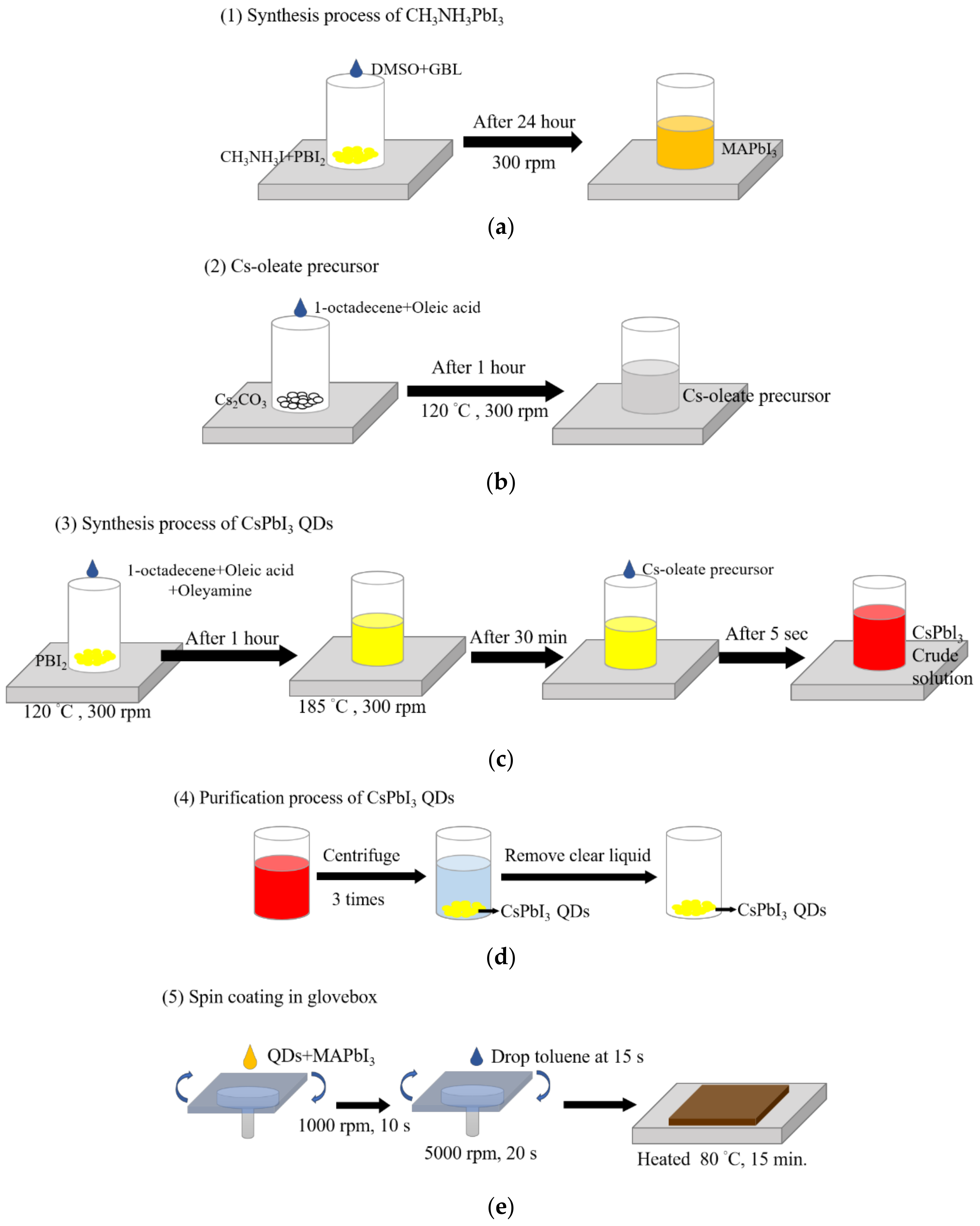
2.2. Solution Preparation and Synthesis for Cs-Oleate Precursor, CsPbI3 QDs, and CH3NH3PbI3

All the experiments were performed in a glove box filled with nitrogen, H2O < 1 ppm and O2 < 1 ppm. The schematic diagram of the experiment is shown in Figure 1.

2.3. Synthesis Process of CH3NH3PbI3

CH3NH3I and PbI2 were mixed into the 50 mL sample bottle, then DMSO and GBL were added into the mixture powder in nitrogen atmosphere and stirred at 300 rpm for 24 h.

2.4. Synthesis Process of Cs-Oleate Precursor

Cs2CO3, OA, and ODE were poured into a 50 mL sample bottle and stirred for 1 h at 120 °C. Then, the Cs-oleate precursor was stored at 100 °C to avoid precipitation.

2.5. Synthesis Process of CsPbI3 QDs

Both 1-octadecene and PbI2 were added into a 50 mL sample bottle and were dried at 120 °C for 1 h. Then, oleic acid and oleyamine were poured. The Cs-oleate precursor was swiftly injected into the solution when the solution was heated to 185 °C. After 5 s, the reaction solution was cooled by ice bath.

2.6. Purification Process of CsPbI3 QDs

MeOAc (the volume ratio of crude solution/Meoac is 1:3) was poured in CsPbI3 crude solution to separate CsPbI3 QDs before centrifuge at 8000 rpm for 5 min. The supernatant solution was removed, and the precipitate was dissolved in 3 mL of hexane. Then, MeOAc (the volume ratio of crude solution/Meoac is 1:1) was added to precipitate CsPbI3 QDs again and centrifuge at 8000 rpm for 2 min. Finally, the QDs were dispersed in 3 mL of hexane and centrifuged at 4000 rpm for 5 min to remove excess PbI2 and precursors. CsPbI3 QDs can be separated after centrifugation to remove the transparent liquid.

2.7. Fabrication of Thin Films

MAPbI3 (50 μL) and CsPbI3 QDs (1 mg) were mixed and spin-coated on a glass substrate in a glove box. The composite perovskite film was annealed at 80 °C for 15 min, then the films were treated by APT for different powers for 2 s, as shown in Table 2.

2.8. Characteristic Measurements

The absorption spectrum of the thin film is measured by ultraviolet/visible (UV/vis) absorption spectroscopy (HITACHI, U-3900, Tokyo, Japan). The crystalline of the thin film is measured by grazing incidence X-ray diffraction (GIXRD; Bruker, D8 Discover, Billerica, MA, USA). The surface roughness of films was measured by atomic force microscopy (AFM; Park Systems, XE-70, Suwon, South Korea). The surface morphology of the thin film is measured by scanning electron microscope (SEM; JEOL, 6330, Tokyo, Japan).

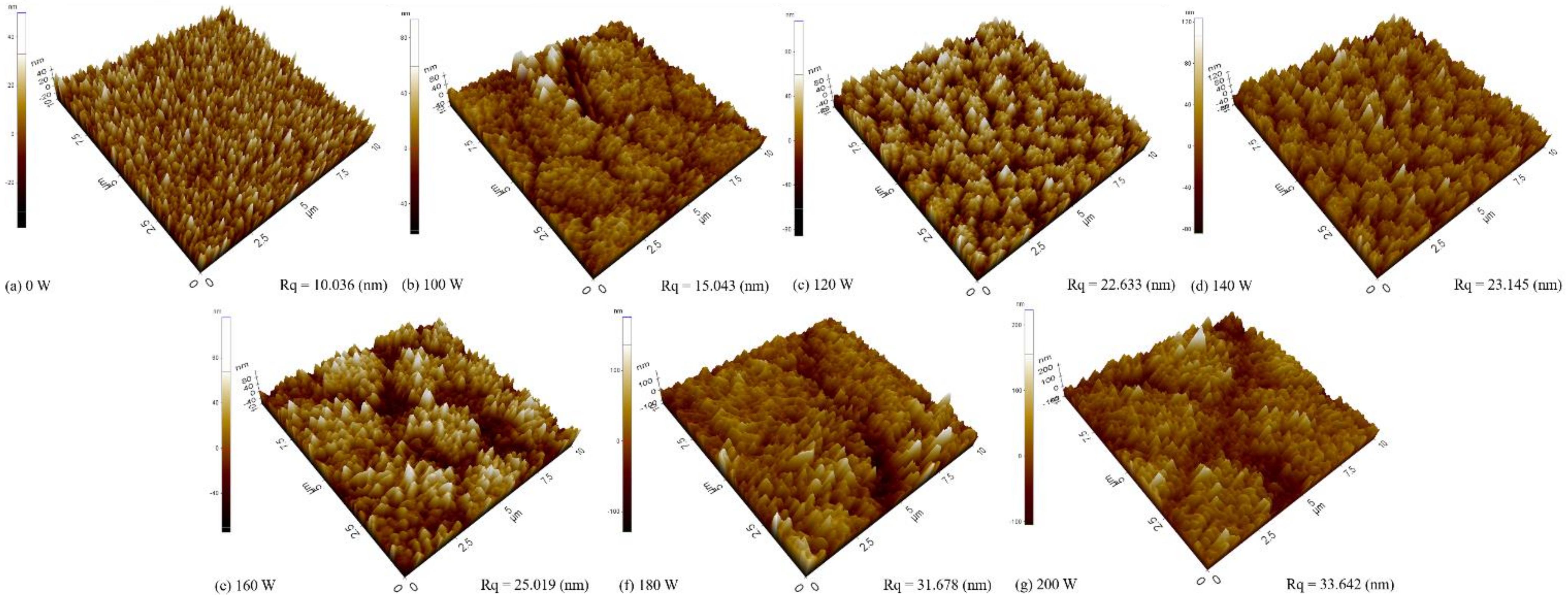
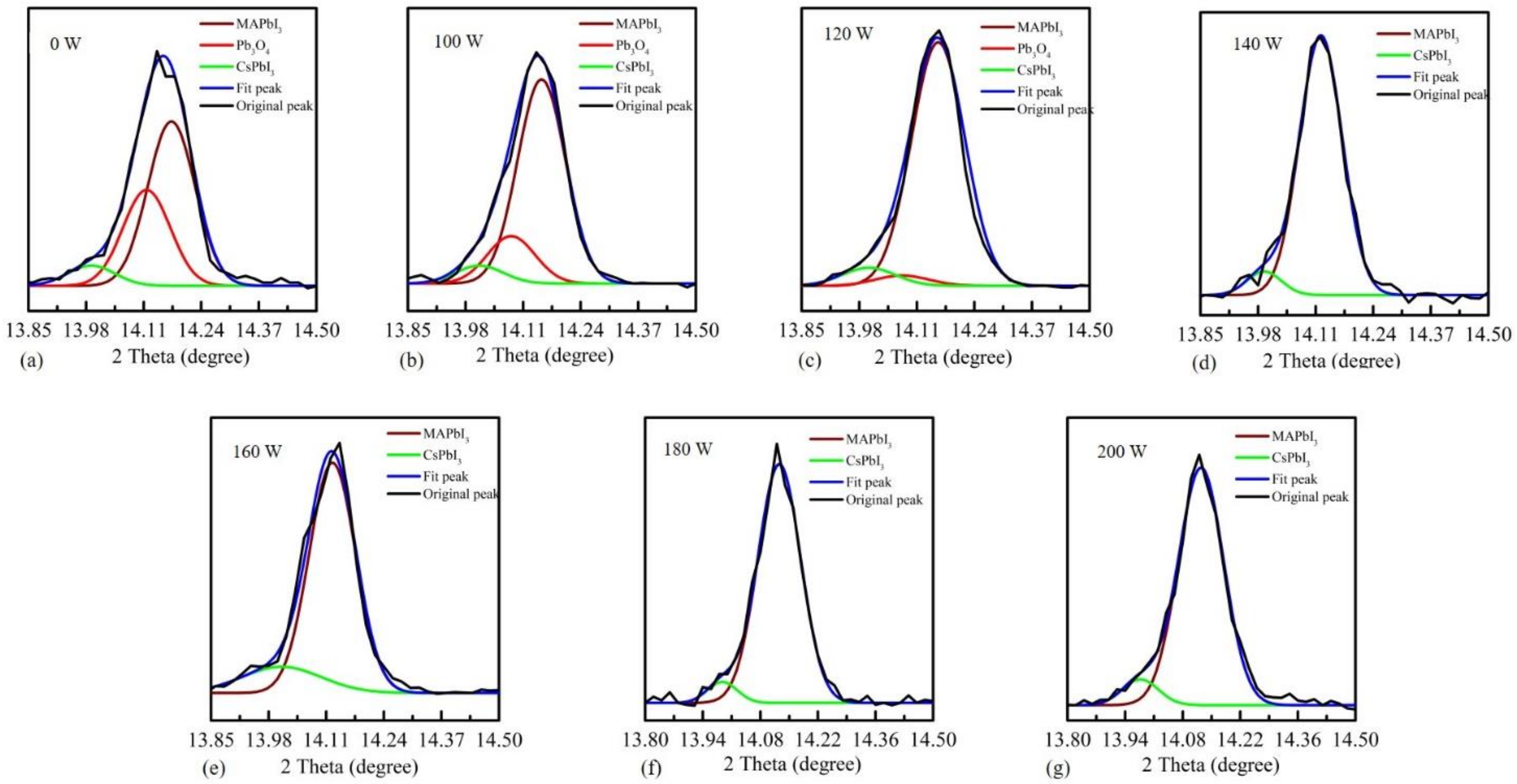
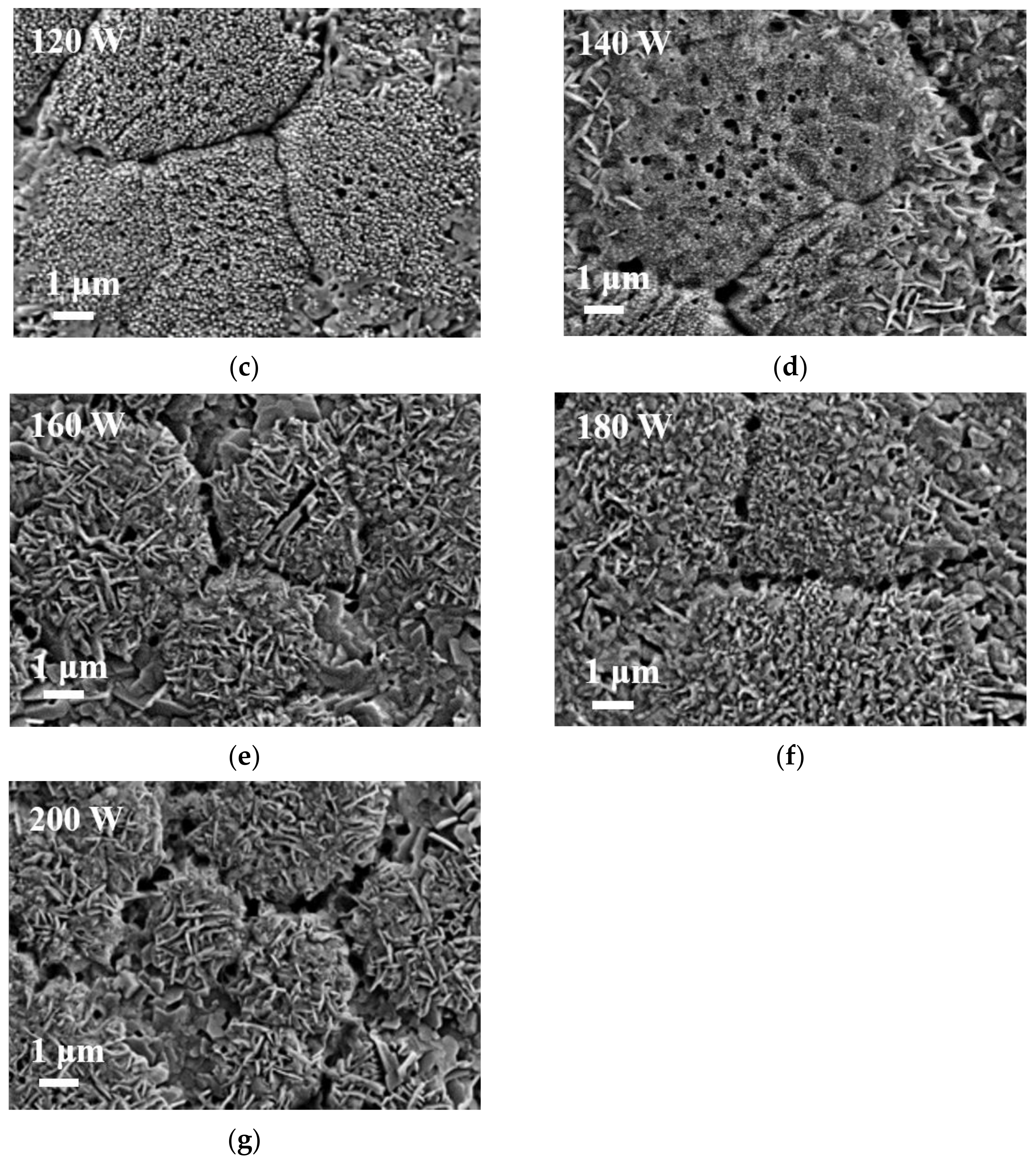
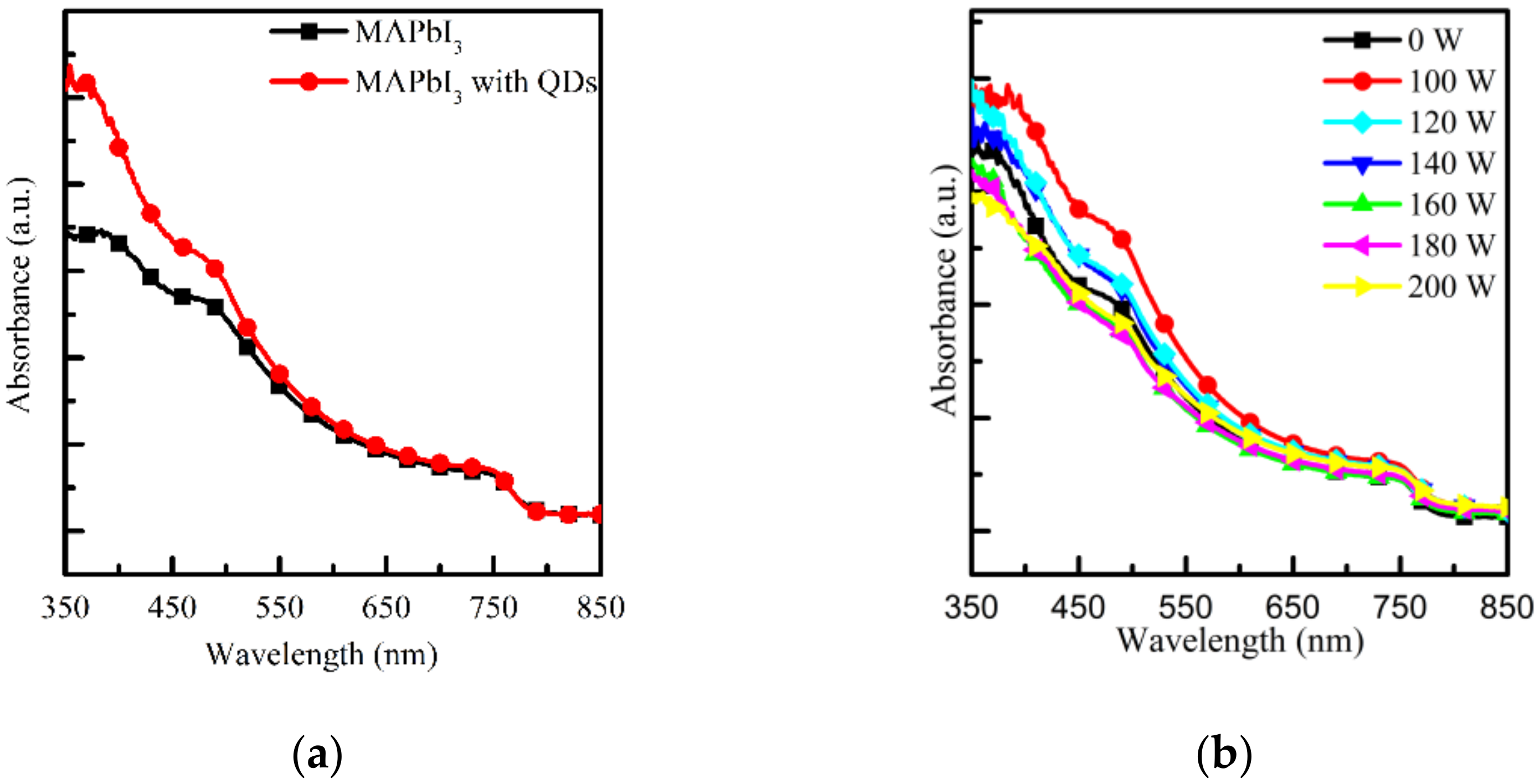
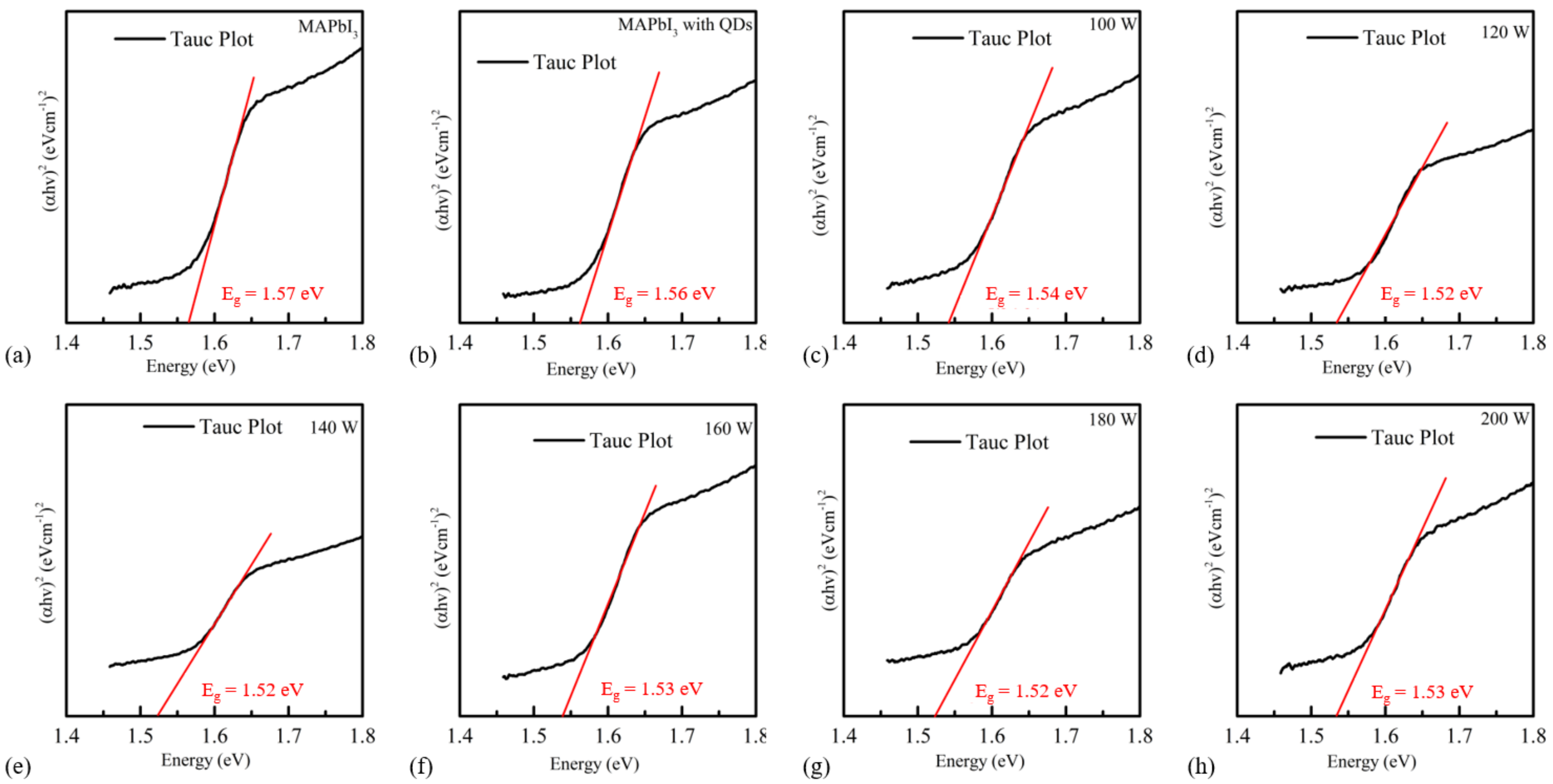
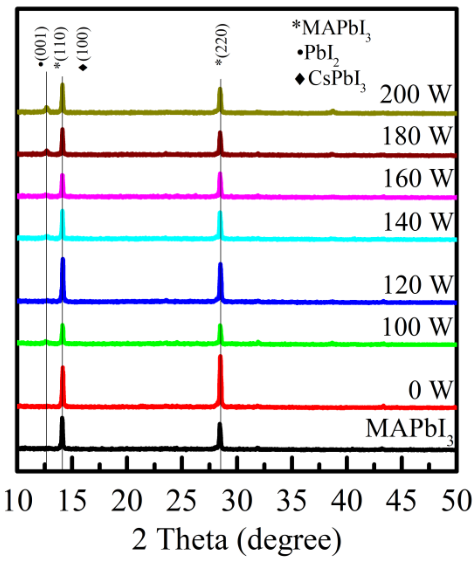
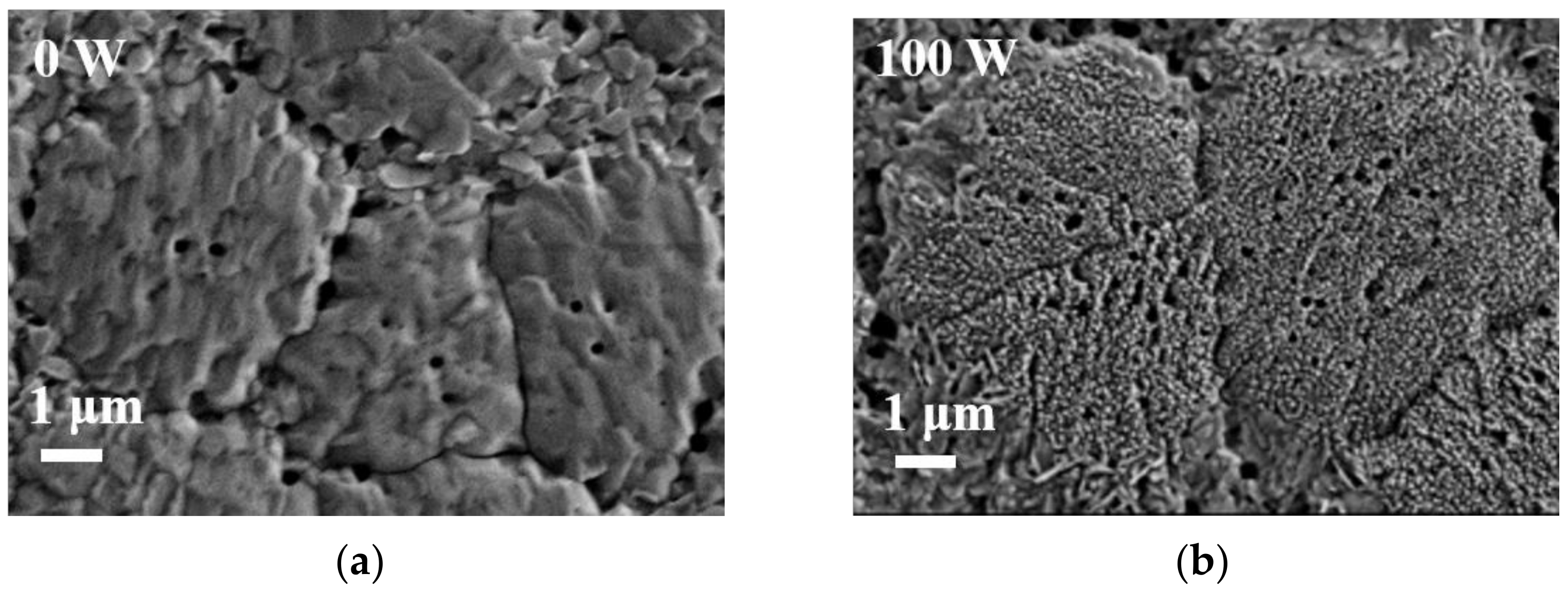
3. Results and Discussion

Figure 2a shows that the absorbance spectrum of the perovskite film with and without CsPbI3 QDs in the wavelength range from 350 to 850 nm.
It can be observed that the absorbance area of the composite perovskite film is larger than that of the pure MAPbI3 film. The reason is that CsPbI3 QDs enhance the absorbance of MAPbI3 at short wavelengths. The α-CsPbI3 QDs is a wide energy gap material, so α-CsPbI3 QDs have stronger absorbance at short wavelengths [16,17].
The surface of composite perovskite films is further optimized via APT at different powers, from 100 to 200 W, as shown in Figure 2b. Absorbance of composite perovskite film is enhanced after the composite perovskite film is treated by APT at 100 W to 140 W. The reason was that APT causes an increase for the roughness of composite perovskite films and a decrease for the band-gap of composite perovskite films.
However, the absorbance will not gradually increase as the wattage increases. When the plasma power is over 160 W, the surface of MAPbI3 film was degraded to PbI2, resulting in a small amount of macula appearing on the surface of the composite perovskite film [9].
To discuss the reasons for the increasing of the absorbance area, tauc plots were obtained from absorption data, as shown in Figure 3.
The band gap of composite perovskite materials was determined by the tauc’s relation as below.
α h v = C h v E g n
where α is the absorption coefficient, Eg is the band gap, is the incident photon energy, C is a constant, and n is the index, which can have different values (2 and 1/2) corresponding to direct allowed transitions and indirect allowed transitions [18,19,20,21].
The band gap of pure MAPbI3 and composite perovskite films are 1.57 eV and 1.56 eV. When composite perovskite films were treated by APT, the band gap is further reduced to 1.52 eV.
The argon plasma removes the oxygen contamination from the surface of the composite perovskite film and changes the values of the valence band and the conduction band.
When composite perovskite films are treated by APT, the valence band will enlarge and the conduction band will shrink, and the film has a lower band gap which is more conducive to capturing sunlight [12,18]. Furthermore, the report also proved that the lower band gap has better photoelectric properties [19,20].
Roughness of composite perovskite film is increased with increasing argon plasma, as shown in Figure 4. The bombardment of the APT caused fine holes on the surface of the composite perovskite film, and the absorbance of the film could be enhanced by these holes. The reason is that the incident beam is mostly scattered, and the absorption is performed again at the holes to enhance the intensity of harvesting [15].
To investigate the argon plasma effect on the crystal phase of the composite film, the X-ray diffraction (XRD) was measured. Figure 5 shows that the XRD pattern of the composite perovskite films were treated by argon plasma at different powers.
Inorganic CsPbI3 QDs can further reduce the degradation of MAPbI3 [21]. The reason is interactions with organic and inorganic functional groups stabilize the perovskite structure [9].
However, the peaks of PbI2 can be observed for 180 W and 200 W curves, indicating that the power of 180 W and 200 W is too high, leading to the degradation of MAPbI3, and PbI2 will affect the efficiency of the perovskite film. Furthermore, there is no peak of metal lead at 31.5° and 36.3°, which means that the plasma treatment of 100 W to 200 W only affects the surface of the perovskite film and does not affect the entire perovskite film [14].
Figure 6 shows the XRD peak fitting patterns of composite perovskite treated by argon plasma at different powers. The peaks are represented in the (100) orientation of CsPbI3 at 13.97°, the (110) orientation of Pb3O4 at 14.05°, and the (110) orientation of MAPbI3 at 14.16°, respectively [22,23]. The presence of the oxygen pollutant Pb3O4 can be observed in Figure 6a. The reason is that oxygen can interact with one or two photoexcited electrons and form superoxide and peroxide. These highly oxidative species react with the inorganic lattice and destroy the Pb-I octahedra by forming Pb-O bonds. The Pb3O4 content is gradually reduced when using APT on composite perovskite, as shown in Figure 6b,c. The Pb3O4 content is completely removed when APT wattage is increased to 140 W, as shown in Figure 6d. This proves that argon plasma is an effective method to remove oxygen contaminants, preventing formation of superoxide and peroxide, and improving film stability and charge carrier life [24,25].
Figure 7 shows scanning electron microscope (SEM) images of films treated with APT at different powers to further analyze their crystalline growth. In Figure 7a, the initial crystal islands and obvious grain boundaries can be observed. As shown in Figure 7b,c, when the power increased to 100 W and 120 W, the bombardment of the argon plasma caused fine holes on the surface of the film, and these holes can increase the light absorption area of the film as previously mentioned in Figure 4. The cause is that the incident beam is scattered roughly, thus increasing the absorption of the sample [14]. In Figure 7d,e, branch-shaped nicks began to appear around the crystal island, and the nicks of the branch-shaped became more obvious as the plasma power increased. As shown in Figure 7f,g, when the wattage continues to increase, a small amount of flaky debris appears around the crystal island. These fragments can be speculated to be PbI2 [26], but the MAPbI3 islands can still maintain their form. This means that the plasma treatment of 100 W to 200 W will only affect the surface of the perovskite film, which is consistent with the XRD measurement results.

4. Conclusions

In this research, the absorbance of composite perovskite film is increased by adding CsPbI3 QDs and APT. In the XRD observation, it was found that there are PbI2 peaks at 180 W and 200 W, indicating that the high plasma wattage causes degradation of MAPbI3. It is observed from SEM that high wattage will damage the surface, so the better parameter is 140 W. From the above analysis, the improved composite film is more stable. Following surface treatment by argon plasma, the light absorption is further improved, which is a good development for perovskite solar cells.

Author Contributions

Conceptualization, S.-Y.L. (Shui-Yang Lien), P.-W.S., N.-F.W. and S.-Y.L. (Shao-Yu Liu); Formal analysis, S.-Y.L. (Shui-Yang Lien), S.-Y.L. (Shao-Yu Liu), and C.-J.H.; Funding acquisition, S.-Y.L. (Shao-Yu Liu) and S.-Y.L. (Shui-Yang Lien); Investigation, S.-Y.L. (Shui-Yang Lien) and C.-J.H.; Resources, S.-Y.L. (Shao-Yu Liu); Supervision, W.-R.C., S.-Y.L. (Shui-Yang Lien), C.-H.L., N.-F.W. and C.-J.H.; Writing—original draft, S.-Y.L. (Shao-Yu Liu). All authors have read and agreed to the published version of the manuscript.

Funding

This work is sponsored by the Ministry of Science and Technology (MOST) of the Republic of China under contact no. 110-2221-E-390-019.

Institutional Review Board Statement

This study did not involve humans or animals.

Informed Consent Statement

This study did not involve humans.

Data Availability Statement

The data presented in this study are available on request from the corresponding author.

Conflicts of Interest

The authors declare no conflict of interest.

References

  1. Chen, Q.; de Marco, N.; Yang, Y.; Song, T.; Chen, C.; Zhao, H.; Hong, Z.; Zhou, H.; Yang, Y. Under the spotlight: The organ-ic–inorganic hybrid halide perovskite for optoelectronic applications. Nano Today 2015, 10, 355–396. [Google Scholar] [CrossRef] [Green Version]
  2. Song, T.B.; Chen, Q.; Zhou, H.; Jiang, C.; Wang, H.H.; Yang, Y.M.; Liu, Y.; Yang, Y. Perovskite solar cells: Film formation and properties. J. Mater. Chem. A 2015, 3, 9032–9050. [Google Scholar] [CrossRef]
  3. Zhou, D.; Zhou, T.; Tian, Y.; Zhu, X.; Tu, Y. Perovskite-Based Solar Cells: Materials, Methods, and Future Perspectives. J. Nanomater. 2018, 2018, 8148072. [Google Scholar] [CrossRef]
  4. Wang, H.; Kim, D.H. Perovskite-based photodetectors: Materials and devices. Chem. Soc. Rev. 2017, 46, 5204–5236. [Google Scholar] [CrossRef] [PubMed]
  5. Zheng, C.; Rubel, O. Unraveling the water degradation mechanism of CH3NH3PbI3. J. Phys. Chem. C 2019, 123, 19385–19394. [Google Scholar] [CrossRef] [Green Version]
  6. Chi, W.; Banerjee, S.K. Achieving Resistance against Moisture and Oxygen for Perovskite Solar Cells with High Efficiency and Stability. Chem. Mater. 2021, 33, 4269–4303. [Google Scholar] [CrossRef]
  7. Li, M.; Zhang, Y.; Tang, X.; Li, J.; Wang, S.; Li, T.; Wang, Q.; Zhao, H.; Li, Q.; Yao, J. Improving performance of hybrid perov-skite/graphene-based photodetector via hot carriers injection. J. Alloys Compd. 2022, 895, 162496. [Google Scholar] [CrossRef]
  8. Deng, X.; Cao, Z.; Li, C.; Wang, S.; Hao, F. Benzotriazole derivative inhibits nonradiative recombination and im-proves the UV-stability of inverted MAPbI3 perovskite solar cells. J. Energy Chem. 2022, 65, 592–599. [Google Scholar] [CrossRef]
  9. Huang, P.H.; Wang, C.W.; Lien, S.Y.; Lee, K.W.; Wang, N.F.; Huang, C.J. Investigation of the Stability of Me-thylammonium Lead Iodide (MAPbI3) Film Doped with Lead Cesium Triiodide (CsPbI3) Quantum Dots under an Oxygen Plasma Atmosphere. Molecules 2021, 26, 2678. [Google Scholar] [CrossRef]
  10. Chen, L.; Cao, H.; Wang, S.; Luo, Y.; Tao, T.; Sun, J.; Zhang, M. Efficient air-stable perovskite solar cells with a (FAI) 0.46 (MAI) 0.40 (MABr) 0.14 (PbI2) 0.86 (PbBr2) 0.14 active layer fabricated via a vacuum flash-assisted method under RH> 50%. RSC Adv. 2019, 9, 10148–10154. [Google Scholar] [CrossRef] [Green Version]
  11. Clark, C.P.; Voigt, B.; Aydil, E.S.; Holmes, R.J. Carrier-gas assisted vapor deposition for highly tunable mor-phology of halide perovskite thin films. Sustain. Energy Fuels 2019, 3, 2447–2455. [Google Scholar] [CrossRef]
  12. Shekargoftar, M.; Pospisil, J.; Dugáček, J.; Weiter, M.; Homola, T. Surface Property Tuning of Methylammonium Lead Iodide by Plasma for Use in Planar Perovskite Solar Cells. ACS Omega 2020, 5, 18384–18390. [Google Scholar] [CrossRef]
  13. Oka, D.; Hirose, Y.; Fukumura, T.; Hasegawa, T. Heteroepitaxial growth of perovskite CaTaO2N thin films by ni-trogen plasma-assisted pulsed laser deposition. Cryst. Growth Des. 2014, 14, 87–90. [Google Scholar] [CrossRef]
  14. Xiao, X.; Bao, C.; Fang, Y.; Dai, J.; Ecker, B.R.; Wang, C.; Lin, Y.; Tang, S.; Liu, Y.; Deng, Y.; et al. Argon Plasma Treatment to Tune Perovskite Surface Composition for High Efficiency Solar Cells and Fast Photodetectors. Adv. Mater. 2018, 30, 5176. [Google Scholar] [CrossRef]
  15. Moreno-Romero, P.M.; Corpus-Mendoza, A.N.; Millán-Franco, M.A.; Rodríguez-Castañeda, C.A.; Torres-Herrera, D.M.; Liu, F.; Hu, H. Roughness and structural modification of PbI2 thin films by isopropanol treatment to improve me-thylammonium lead halide formation and solar cell efficiency. J. Mater. Sci. Mater. Electron. 2019, 30, 17491–17503. [Google Scholar] [CrossRef]
  16. Smith, A.; Mohs, A.; Nie, S. Tuning the optical and electronic properties of colloidal nanocrystals by lattice strain. Nat. Nanotechnol. 2008, 4, 56–63. [Google Scholar] [CrossRef] [Green Version]
  17. Luo, S.; Kazes, M.; Lin, H.; Oron, D. Strain-induced type II band alignment control in CdSe nanoplate-let/ZnS-sensitized solar cells. J. Phys. Chem. C 2017, 121, 11136–11143. [Google Scholar] [CrossRef]
  18. Shekargoftar, M.; Jurmanová, J.; Homola, T. A study on the effect of ambient air plasma treatment on the proper-ties of methylammonium lead halide perovskite films. Metals 2019, 9, 991. [Google Scholar] [CrossRef] [Green Version]
  19. Wang, T.; Zhang, H.; Hou, S.; Zhang, Y.; Li, Q.; Zhang, Z.; Gao, H.; Mao, Y. Facile Synthesis of Methylammonium Lead Iodide Perovskite with Controllable Morphologies with Enhanced Luminescence Performance. Nanomaterials 2019, 9, 1660. [Google Scholar] [CrossRef] [Green Version]
  20. Da Silva Filho, J.M.C.; Ermakov, V.A.; Marques, F.C. Perovskite thin film synthesised from sputtered lead sul-phide. Sci. Rep. 2018, 8, 1563. [Google Scholar] [CrossRef]
  21. Lien, S.-Y.; Chen, Y.-H.; Chen, W.-R.; Liu, C.-H.; Huang, C.-J. Effect of Growth Temperature on the Characteristics of CsPbI3-Quantum Dots Doped Perovskite Film. Molecules 2021, 26, 4439. [Google Scholar] [CrossRef]
  22. Liu, T.; Hu, Q.; Wu, J.; Chen, K.; Zhao, L.; Liu, F.; Wang, C.; Lu, H.; Jia, S.; Russell, T.; et al. Mesoporous PbI2 Scaffold for High-Performance Planar Heterojunction Perovskite Solar Cells. Adv. Energy Mater. 2015, 6, 1501890. [Google Scholar] [CrossRef]
  23. Yousefi, R.; Soofivand, F.; Salavati-Niasari, M. PbHgI4/HgI2 nanocomposite: Simple synthesis, characterization and electrochemical and optical properties. J. Mater. Sci. Mater. Electron. 2016, 28, 2615–2623. [Google Scholar] [CrossRef]
  24. Qiao, L.; Fang, W.H.; Prezhdo, O.V.; Long, R. Suppressing Oxygen-Induced Deterioration of Metal Halide Perov-skites by Alkaline Earth Metal Doping: A Quantum Dynamics Study. J. Am. Chem. Soc. 2022, 144, 5543–5551. [Google Scholar] [CrossRef] [PubMed]
  25. Kong, W.; Rahimi-Iman, A.; Bi, G.; Dai, X.; Wu, H. Oxygen Intercalation Induced by Photocatalysis on the Surface of Hybrid Lead Halide Perovskites. J. Phys. Chem. C 2016, 120, 7606–7611. [Google Scholar] [CrossRef]
  26. Watthage, S.C.; Song, Z.; Liyanage, G.K.; Phillips, A.B.; Heben, M.J. Investigation on the nucleation and growth mechanisms of perovskite formation in the two-step solution process. In Proceedings of the 2016 IEEE 43rd Photovoltaic Specialists Conference (PVSC), Portland, OR, USA, 5–10 June 2016. [Google Scholar]
Figure 1. (ae) Schematic diagram of perovskite, perovskite quantum dots, and fabrication of thin film.
Crystals 12 00799 g001
Figure 2. Absorbance of UV–visible light spectra of perovskite film (a) MAPbI3 and MAPbI3 composite with QDs without APT (b) MAPbI3 composite with QDs treated by APT at different powers.
Crystals 12 00799 g002
Figure 3. (ah) Band-gap calculation for MAPbI3 and composite perovskite film treated by APT at different powers.
Crystals 12 00799 g003
Figure 4. AFM images of perovskite films composed of MAPbI3 and CsPbI3 QDs treated at different argon plasma powers, from (ag) 0–200 W.
Crystals 12 00799 g004
Figure 5. XRD patterns of MAPbI3 and composite perovskite film treated by argon plasma at different powers.
Crystals 12 00799 g005
Figure 6. (ag) XRD fitting patterns of composite perovskite treated by argon plasma at different powers.
Crystals 12 00799 g006
Figure 7. Top-view SEM images of perovskite films composed of MAPbI3 and CsPbI3 QDs treated at different argon plasma powers, from (ag) 0–200 W.
Crystals 12 00799 g007aCrystals 12 00799 g007b
Table 1. Preparation parameters of CH3NH3PbI3, Cs-oleate precursor, and CsPbI3 QDs.
Synthesis of CH3NH3PbI3Cs-Oleate PrecursorSynthesis of CsPbI3 QDs
CH3NH3I 198.75 mgCs2CO3 0.1 gPbI2 0.173 g
GBL(C4H6O2) 0.5 mLOleic acid 0.5 mL1-octadecene 10 mL
PbI2 576.25 mg1-octadecene 10 mLOleic acid 1 mL
DMSO(C2H6OS) 0.5 mL Oleyamine 1 mL
Cs-oleate precursor 1.6 mL
Table 2. Types of film and power range of argon plasma.
FilmPower
MAPbI30 W
MAPbI3 with QDs0 W
MAPbI3 with QDs100 W
MAPbI3 with QDs120 W
MAPbI3 with QDs140 W
MAPbI3 with QDs160 W
MAPbI3 with QDs180 W
MAPbI3 with QDs200 W
Publisher’s Note: MDPI stays neutral with regard to jurisdictional claims in published maps and institutional affiliations.

