Article

Twist Angle-Dependent Interlayer Exciton in MoS2 Bilayers Revealed by Room-Temperature Reflectance

1
Centre for Quantum Physics, Key Laboratory of Advanced Optoelectronic Quantum Architecture and Measurement (MOE), School of Physics, Beijing Institute of Technology, Beijing 100081, China
2
Beijing Key Laboratory of Nanophotonics and Ultrafine Optoelectronic Systems, Beijing Institute of Technology, Beijing 100081, China
*
Authors to whom correspondence should be addressed.
Crystals 2022, 12(6), 761; https://doi.org/10.3390/cryst12060761
Submission received: 24 April 2022 / Revised: 22 May 2022 / Accepted: 24 May 2022 / Published: 25 May 2022
(This article belongs to the Section Inorganic Crystalline Materials)

Abstract

:
In 2H stacking bilayer MoS2, the exciton with an interlayer nature has been evidenced due to the hybridization of hole states among both layers. The transition energy of this interlayer exciton is located between the A and B excitons. In this work, we investigate the evolution of optical properties in stacking MoS2 bilayers with the twisted angles ranging from 0° to 60°, especially focusing on the interlayer exciton. The clear modulations of the exciton responses are observed by the room-temperature reflectance. The interlayer exciton transition is observed in the artificial stacking bilayer MoS2 with the twisted angle around 60°. We found that the interlayer exciton is very sensitive to the twisted angle. Once the stacking angle deviates the 2H stacking by a few degrees, the interlayer transition is quenched. This is due to the bilayer symmetry and interlayer coupling of this unique system.

1. Introduction

Transition metal dichalcogenides (TMDCs), such as molybdenum disulfide (MoS2), are direct band gap semiconductors in their monolayer limit and indirect band gap semiconductors in bulk form [1,2,3,4]. They possess optical transitions in the visible and near infrared range. The semiconducting properties extend the applications of two-dimensional (2D) materials beyond what graphene achieves alone [5,6,7]. The light–matter interaction in monolayer is governed by Coulomb bound electron–hole pairs, excitons, with exceptionally large binding energy. As the second layer is added, the light matter interaction is strongly modified since the band structure varies and the new interlayer exciton (IE) complexes can form [8,9,10,11]. A bilayer formed by artificial stacking of two monolayers exhibits a crucial degree of freedom—the twisted angle between the layers. The important properties of 2D van der Waals bilayers, such as the valley dynamics [12] and spatial diffusion [13,14,15], are dominated or strongly affected by the twist angle. In the MoSe2/WSe2 heterobilayer, 2° changes in the twist angle could bring one order of magnitude of difference to the interlayer exciton lifetimes [9]. These IEs in TMDC heterostructure have a large out-of-plane permanent dipole, which permit efficient field control in on-chip miniaturized structures [16]. Interestingly, the IE states have been also evidenced in the homobilayer and multilayer system, such as bilayer MoSe2 and MoS2 [17,18,19]. Due to the coupling with intralayer excitons, these new type of interlayer excitons have greater oscillator strength. This highly tunable exciton transition holds great potential for the spin-valley physics and nano-scale Moire interactions.
The monolayer of semiconducting TMDCs is arranged in a trigonal prismatic structure, where the inversion symmetry is absent. Due to the rotation symmetry of a TMDCs monolayer, different situations are represented by the stackings with twist angles ranging from 0° to 60°. By tuning the important knob, with a twisted angle, the binding energy of charged exciton and the indirect bandgap in MoS2 bilayers were found to be efficiently tuned [20,21]. The relative angles are also crucial as the inversion symmetry is restored (still lacking) in the 2H (3R) stacking. Theoretical and experimental studies have shown that varying the interlayer twist angle could allow or remove the interlayer hopping, and thus control the interlayer coupling and introduce the interlayer exciton in 2H MoS2 bilayers [17,19,22]. The interlayer exciton possesses a higher (20%) oscillator strength of the intralayer exciton, which allows the absorption or reflectivity detections. As the hole state of the IE is delocalized over the two layers, the transition energy is typically larger than the intralayer K-K exciton energy. This is different from the WSe2 bilayer system, where the IE energy is lower than the intralayer ones, at about 150 meV [12,23]. In bilayer WSe2, the interlayer transition arises from the K–Q transition. The Q state (more delocalization than K) in the conduction band is at lower energy and thus the corresponding IE transition. The previous studies of the IE in bilayer MoS2 have focused on the H or R stacking at cryogenic temperatures [17,19]. In the hBN encapsulated artificially stacked twist-angle bilayers, the IE PL emission was observed at low temperatures that appear only at the 62° sample [24]. This IE emission was not clearly detectable at the evaluated temperature, as the relaxations to lower intralayer emissions or the non-radiative channels are active. Thus, room-temperature, easily performed measurements to investigate the interlayer coupling and the IE would still be favorable.
In this paper, we show that the reflectance of the artificially stacked MoS2 samples on the transparent substrates is sufficient to reveal such effects. Without the hBN encapsulation, we directly fabricate MoS2 bilayer samples with the twist angles ranging from 0° to 60° using angle-resolved dry transfer system. The exciton transitions are characterized by the reflectance measurements. By selectively positioning one layer of MoS2 onto another one, we found the IE transition can be restored and tuned. The A–B exciton splitting energy is around 140 meV for bilayers with twist angles from 0° to 55°’ however, this increased to 170 meV for the 2H stackings. This reflects the valence band interlayer coupling. The IE transition is active only at the twisted angles that are close or equal to the 2H stacking, which is due to the strict symmetry conditions of the interlayer coupling of hole states. Our results indicate that the up boundary of the deviation should be around ±3°.

2. Experimental Method

In this work, monolayer and bilayer MoS2 were fabricated by the mechanical exfoliation with adhesive tape from a bulk crystal (2D semiconductors, Inc., USA). Then, the samples were transferred onto a transparent substrate such as sapphire and quartz with the help of polydimethylsiloxane (PDMS); this is depicted in Figure 1a. Here, the samples are naturally formed 2H MoS2 bilayers, where the top and bottom layers have an equivalent twist angle θ = 60° or 180°. The different twist angles of MoS2 bilayer were achieved by stacking two monolayers with a certain angle determined initially by the regular edges (for details, see Supplementary Materials). The precise twist angles were then determined by the polarization-resolved second-harmonic generation (SHG) measurements. The incident laser is from a mode-locked ultrafast laser, Ti: sapphire laser system (Chameleon Ultra II, Coherent Inc., USA), at 800 nm and is linearly polarized. The SHG signal with parallel polarization component to the excitation laser has a six-fold rotational symmetry pattern. The SHG signals were collected from individual monolayers and bilayer regions using a back-reflection geometry. Depending on the twist angle, the interference of the signals from the top and bottom layers generates SHG with different intensity from the bilayer sample. For example, the SHG intensity will be stronger (weaker) in the 3R (2H) stacking than in the monolayer. By comparing the six-fold pattern of the top and bottom monolayers and the intensity of the homojunction region [25], we can easily deduce the twist angles of the samples. The details of the measurements and results of each sample described in the Supplementary Materials.
The optical spectroscopy was performed by a homemade micro-spectroscopy set-up. The reflectance spectra were measured with a broadband tungsten–halogen lamp as the light source. The signal from the samples was coupled to fiber and then collected through spectrometer with a liquid nitrogen-cooled charge-coupled device detector (PyLoN, Princeton Instruments Inc., USA). All measurements were performed at room temperature. To avoid the damage of samples by heating or by radiation, the laser power was set to the order of microwatts during the measurements of PL or Raman.

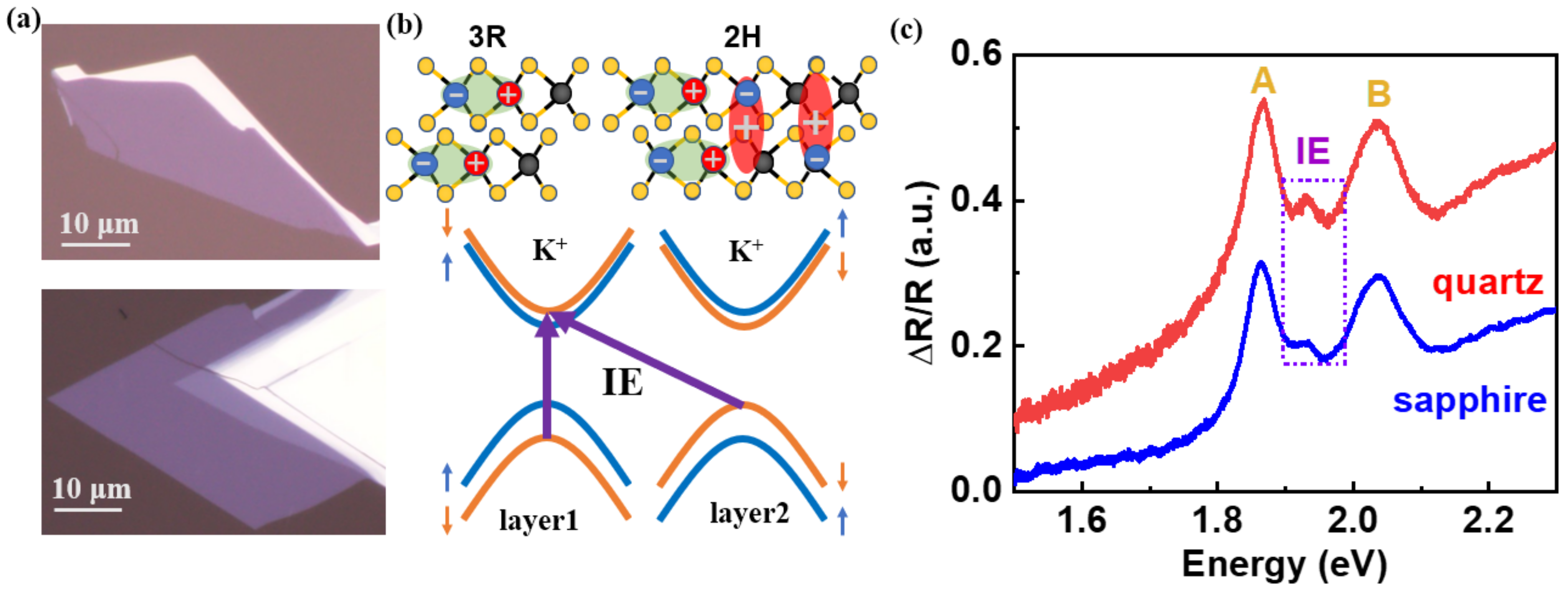
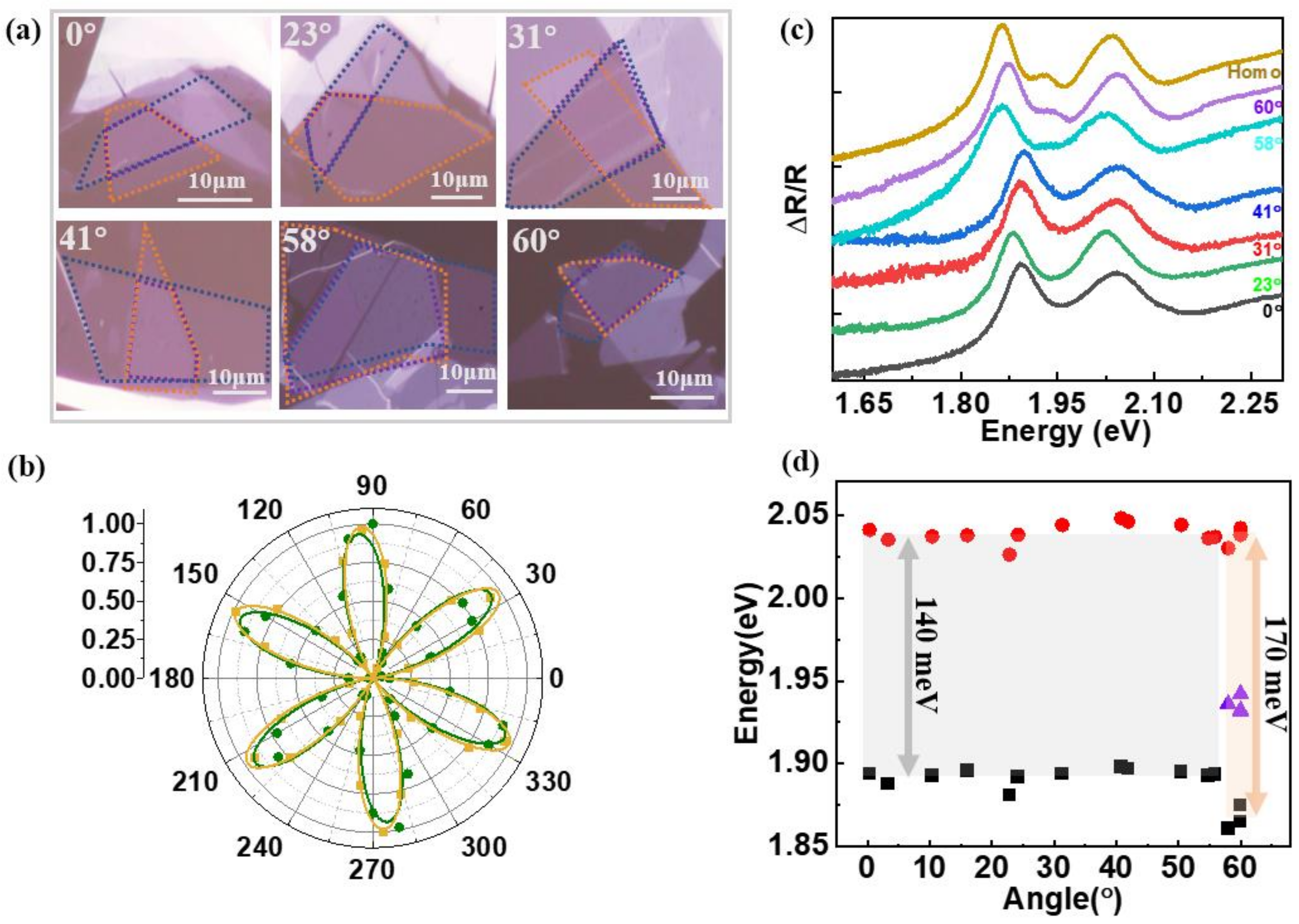
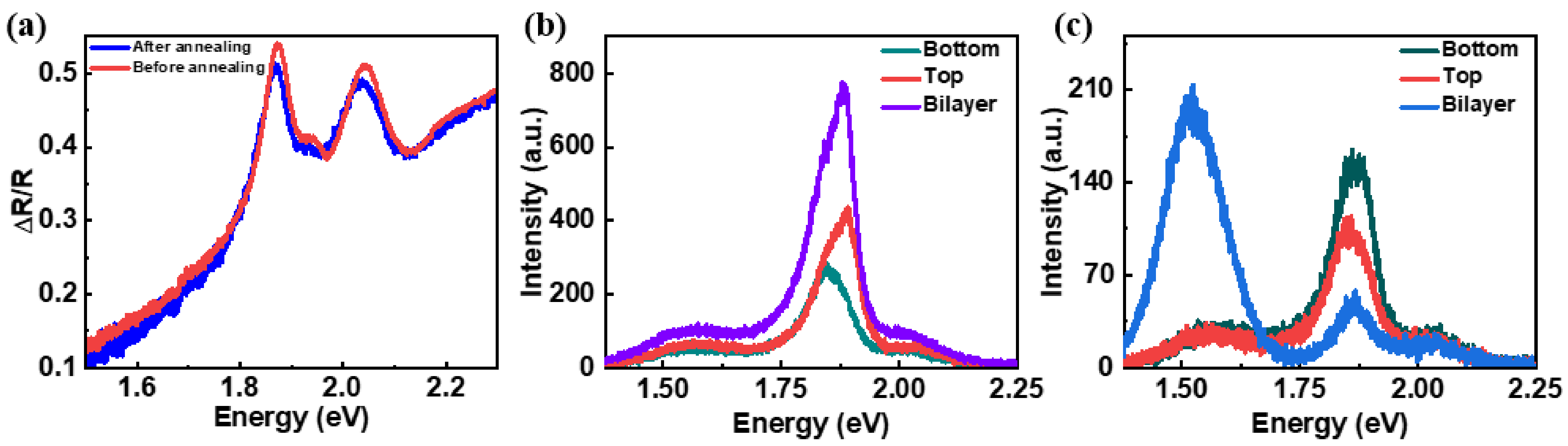
3. Results and Discussion

Optical microscope images of exfoliated MoS2 bilayers on sapphire (upper panel) and quartz (lower panel) substrates are presented in Figure 1a. Here, the samples are the natural 2H bilayers, where the interlayer exciton can be formed with electron in one layer and the hole hybridized over the two, as shown in the upper panel of Figure 1b. The 2H MoS2 bilayers provide an ideal model to investigate the interlayer hybridization of the valance band with the larger band offset from the hopping term [22]. The corresponding interlayer exciton consists of the conduction band (CB) and valence band (VB) edge states at the K points as illustrated in the lower panel of Figure 1b. The hole hybridization of the top VB with the lower energy band in the second layer endows the interlayer large electric dipole. The differential reflectance (ΔR/R) of the bilayer MoS2 is derived from white light reflected from the bilayer sample and the transparent substrate via ΔR/R = (Rsam − Rsub)/Rsam, where Rsam is the intensity reflection coefficient of the sample and Rsub is for the one from sapphire or quartz.
Figure 1c shows the differential reflectance of the homobilayer MoS2 at room temperature on the sapphire and quartz substrate, where three distinct transitions are resolved. The two transitions at 1.88 eV and 2.05 eV are assigned to the intralayer A and B excitons, respectively. In the monolayer, the A and B exciton transitions originate from direct transitions at the K point of the Brillouin zone, where a large VB splitting presents due to the strong spin–orbit coupling in TMDCs. However, in the optical measurements this energy splitting will be modified by the different exciton binding energies. In the R stacking MoS2 bilayers, this A–B exciton splitting energy will be a similar value to the interlayer hole hopping vanished. As shown in Figure 1c, the 170 meV splitting is larger than the typical spin–orbit coupling energy that is around 140 meV. This means that, in our 2H sample, the strong interlayer coupling in the valence band is turned on and the A–B splitting is determined by the band offset and the interlayer hopping [26]. The slight interlayer coupling between the bottom layer valence band and the top layer conduction band is a symmetry allowed by small value, as the larger band is offset [24]. Thus, the typical observed A–B splitting is more or less the same as the monolayer. In addition, the prominent IE response is clearly visible between the A and B excitons at 1.95 eV, i.e., 70 meV above the A exciton, consistent with the previous reports [17,19,24]. The interlayer exciton in 2H MoS2 bilayer is another indicator of the strong interlayer coupling. Since the substrates are transparent, the real absorption A ω could be determined by δ R ω = 4 n s u b 2 1 A ω , where δ R ω is the reflectivity [27]. The reflectance of the samples on quartz is higher than sapphire because of the lower refractive index of quartz. The deduced absorption of the two samples is similar, which is ~15% for A exciton, ~14% for B exciton.
In order to investigate the interlayer coupling in the twisted bilayers, we compare the reflectivity of the 2H homobilayer and the artificial stacking bilayer samples with different twist angles. Figure 2a shows some of the representative twist-angle samples. To determine the precise twist angles, we performed the SHG measurements, as shown in Figure 2b. From this polar plot SHG signal, one can distinguish the zigzag direction but not directly the R or H stacking. We also compare the SHG intensity from the bilayers to the monolayers (for details, see the Supplementary Materials). The R stacking SHG is stronger than the individual single layers, while the H stacking is opposite [28]. The typical reflectance spectra of the selected bilayers on sapphire substrates with twist angles of 0°–60° accompanied with the naturally exfoliated 2H bilayer MoS2 are presented in Figure 2c (referred to as Homo). The interlayer exciton in this homobilayer sample is clearly resolved, while the main absorption features of other twist angle samples are quite similar. The interlayer excitons of the 2H stacked bilayer MoS2 (that is, 60° twisted angle) samples can be observed by differential reflectance spectroscopy. In 3R stacking (i.e., twist angle θ = 0°), there is no interlayer transition. This is because, under this stacking of configurations, the delocalization of the holes is not allowed, resulting in the suppression of hole hopping [21,24].
Next, we focus on the twist angle-dependent IE transition. In the artificial stacking MoS2 bilayers, the IE response is restored when the relative angle is close to 60°, though the angle tolerance is very limited as shown in Figure 2c. For the samples with twisted angles, where deviation from 2H stacking larger than about ±3°, the IE transition disappears. This observation is inconsistent with the low temperature PL results of 62° twisted MoS2 bilayer encapsulated in hBN [24]. As the IE energy is higher than the A exciton, the direct PL intensity is typically weak from this hot emission. Therefore, the encapsulation with atomically flat surface and cryogenic temperature are needed. This is due to the higher oscillator strength of the IE, which allows the detection by absorption or reflectivity (transparent substrates required) at room temperature. In our measurements, the IE signal disappears at about 57°, 3° deviating from the 2H stacking, which means that there is very high angle sensitivity in these IE states. Considering the uncertainty of measurements of twisted angle, we speculate that interlayer excitons in MoS2 bilayers can only be optically observed when the twisted angle is in the range of 60° ± 3°. This angle-sensitive effect can be associated with changes in the interlayer distance between monolayers with different twist angles. In 2014, Wang Feng et al. showed that in bilayer MoS2, the interlayer coupling strength of electronic states near the band edge depends on the interlayer distance and has nothing to do with the lattice alignment in the horizontal direction through theoretical calculations. When the twist angle is 0° and 60°, the interlayer distance is the smallest and the interlayer coupling is the strongest, which is mainly due to the repulsive steric effects [20]. Therefore, the bilayer MoS2 with twist angle around 60° makes it easier to observe the interlayer excitons due to the enhanced interlayer coupling effect. Another crucial reason is that the twist angle causes the momentum space of the two layers to be mismatched, resulting in the inhibition of interlayer hopping [28]. Inside this small angle range, the interlayer control by pressure engineering could be a sufficient strategy to explore the interaction between the IE with out-of-plane dipole and the moiré potential. The reflectance measurements could provide an easy approach as it is compatible with the typical diamond anvil cell [29,30,31].
The typical spin–orbit splitting value in the valence band is about 140 meV in monolayer MoS2. Our results in Figure 2d also demonstrate that the A–B exciton differences are affected by the twist angle. The A–B exciton splitting of 3R stacking and the twist angles between 0° and 55° bilayers are around 140 meV, which is dominated by the valence band spin-orbit coupling energy and is insensitive to the twist angle. The energy splitting of the bilayers around 60° is increased to 170 meV. As theoretical and experimental results demonstrated, the interlayer hybridization exists in the 2H stacking [26,32]. Therefore, this energy is a good indicator of the interlayer coupling, as shown in Figure 2d. The A–B splitting increases after the twist angles increase to larger than 55° and the interlayer exciton appears (purple triangles in Figure 2d). Quantitatively, the interlayer coupling energy can be derived by t = S 2 H 2 Δ SO 2 4 , where the S 2 H denotes the energy splitting of the A–B exciton and the Δ SO is the spin-orbital splitting [32]. Here, we take the values from Figure 2d and obtain the hopping term around 48 meV at a twist angle of around 60°, which is similar as the experimental results [22,24,32] and the calculations [8].
The interlayer quality is one of the key parameters, as the fabrication process may introduce absorbates that decrease the coupling. We note that the absorption intensity of artificially stacked 60° interlayer excitons is slightly weakened relative to the intrinsic 60° sample, which may be due to some contamination during the stacking process, resulting in weakened interlayer coupling, as shown in Figure 2c. Annealing is an effective method that could improve the sample quality to make the stake as a whole system. We annealed those samples using quartz as the substrates under an argon atmosphere 200 °C for 2 h. Figure 3a is the differential reflectance of the bilayer MoS2 with twist angles of 58° before and after annealing. After annealing, the absorptions of A and B excitons are decreased and the relative ratio between the two peaks is reduced. Meanwhile, both of the two peaks are red shifted. The peak width of the two peaks is slightly narrowed after annealing [33]. Our results also suggest that some defects may be introduced in the annealed samples. Figure 3b,c show the PL spectra of bilayer MoS2 with twist angles of 54° and 58° on quartz substrates. At the 54° twist angle, the PL intensity of the A excitons in the bilayer position is more or less the sum of in the two individual monolayers, indicating the weak coupling between the two layers. In stark contrast to the twist angle 58°, the PL intensity is lower in the bilayer region compared to that of the monolayer region, as shown in Figure 3c. The significant emission of the indirect transition arises at about 1.5 eV, which indicates that the bilayer profile is restored with stronger interlayer coupling. It is known that the R and H stackings are the two favorable geometries with the smaller interlayer distance, where the indirect emission is located at lower energy in these two cases [20,24]. The PL result of the samples in our works is in good agreement with this behavior (see Figure S3). The quench of the direct transition PL in Figure 3c arises from the change in the band type after the stacking. However, in some of our bilayer MoS2 with 60° twisted angles, the PL intensity is doubled compared to the monolayers. Meanwhile, the A–B exciton splitting is measured at about 150 meV. These two observations are consistent, which means that the real coupling is absent. We note that the sufficient evaluation of interface quality of TMDCs stacks should be on account of the combined analysis of reflectance, PL and the band details. In our work, the samples were fabricated by the simple stacking and the general annealing process. This type of sample is suitable for microscopic optical measurements with a moderate homogeneity across the bilayer regions (see Figure S4). Nevertheless, optimizing the van der Waals stacks for the transport measurements or large-area applications requires a special process.

4. Conclusions

In this work, we investigate the optical properties of MoS2 bilayers with different twist angles focusing on the interlayer coupling effects. The strongest coupling has been observed in stacked MoS2 bilayers with twist angles close to 60°, which well reproduce the structure of 2H form in natural MoS2. In both exfoliated and artificially stacked MoS2 bilayers, the IE transition is well resolved by reflectance at room temperature. Simultaneously, the larger A–B exciton splitting appears when the twist angle approaches 60°. These results indicate that the interlayer hole hopping is very sensitive to the relative twisted angle, where only a few degrees could completely turn off the coupling due to the strict symmetry condition. Our work emphasises the twist angle as an efficient knob for the interlayer engineering of the van der Waals homobilayers.

Supplementary Materials

The following supporting information can be downloaded at: https://www.mdpi.com/article/10.3390/cryst12060761/s1, Figure S1-1: Schematics of the transfer process; Figure S1-2: (a–n) Optical microscopy images of twisted bilayer MoS2 with the twist angle of 0°, 3°, 10°, 16°, 23°, 24°, 31°, 41°, 42°, 50°, 55°, 56°, 58° and 60°, respectively. The yellow dotted line represents the upper monolayer MoS2, the blue dotted line represents the bottom monolayer MoS2, and the purple dotted line represents the twist angle bilayer region; Figure S2: Left. Polar plot for PSHG from the top (black square) and bottom (red circle) layers of each sample, the solid line (black for top layers and red for bottom) is the corresponding fitting curve. Right. The SHG intensity for monolayer regions and homojunction regions. (a–n) represents the samples at a twist angle of 0°, 3°, 10°, 16°, 23°, 24°, 31°, 41°, 42°, 50°, 55°, 56°, 58° and 60°, respectively; Figure S3: Twist angle-dependent energy positions of indirect excitons obtained by Gaussian fitting of PL spectra; Figure S4: (a–c) Optical microscopy image of MoS2 bilayer with the twist angles of 10°, 23° and 60°, respectively. The numbers represent the different positions where the PL are detected. (d–f) PL spectra of different positions correspond to the positions in (a–c), respectively.

Author Contributions

Conceptualization, B.N. and G.W.; methodology, L.X., T.T., X.F. and H.L.; validation, P.Z., X.Z., W.Q. and L.X.; formal analysis, L.X. and B.N.; investigation, L.X. and T.T. and X.F.; resources, Q.W., Z.W. and G.W.; data curation, L.X. and B.N.; writing—original draft preparation, L.X. and B.N.; writing—review and editing, B.N. and G.W.; visualization, L.X. All authors have read and agreed to the published version of the manuscript.

Funding

This research was funded by the National Natural Science Foundation of China (Grants No. 11904019, 12074033, 12074036, 92065109), the Beijing Natural Science Foundation (Grant No. Z190006).

Institutional Review Board Statement

Not applicable.

Informed Consent Statement

Not applicable.

Data Availability Statement

The data presented in this study are available on request from the corresponding author.

Conflicts of Interest

The authors declare no conflict of interest.

References

  1. Gong, Y.; Lin, J.; Wang, X.; Shi, G.; Lei, S.; Lin, Z.; Zou, X.; Ye, G.; Vajtai, R.; Yakobson, B.I.; et al. Vertical and in-Plane Heterostructures from WS2/MoS2 Monolayers. Nat. Mater. 2014, 13, 1135–1142. [Google Scholar] [CrossRef] [PubMed] [Green Version]
  2. Plechinger, G.; Nagler, P.; Kraus, J.; Paradiso, N.; Strunk, C.; Schüller, C.; Korn, T. Identification of Excitons, Trions and Biexcitons in Single-Layer WS2. Phys. Status Solidi R 2015, 9, 457–461. [Google Scholar] [CrossRef] [Green Version]
  3. Withers, F.; Bointon, T.H.; Hudson, D.C.; Craciun, M.F.; Russo, S. Electron Transport of WS2 Transistors in a Hexagonal Boron Nitride Dielectric Environment. Sci. Rep. 2014, 4, 4967. [Google Scholar] [CrossRef] [Green Version]
  4. Sorkin, V.; Pan, H.; Shi, H.; Quek, S.Y.; Zhang, Y.W. Nanoscale Transition Metal Dichalcogenides: Structures, Properties, and Applications. Crit. Rev. Solid State 2014, 39, 319–367. [Google Scholar] [CrossRef]
  5. Komsa, H.P.; Kotakoski, J.; Kurasch, S.; Lehtinen, O.; Kaiser, U.; Krasheninnikov, A.V. Two-Dimensional Transition Metal Dichalcogenides under Electron Irradiation: Defect Production and Doping. Phys. Rev. Lett. 2012, 109, 035503. [Google Scholar] [CrossRef] [PubMed]
  6. Wang, Q.H.; Kalantar-Zadeh, K.; Kis, A.; Coleman, J.N.; Strano, M.S. Electronics and Optoelectronics of Two-Dimensional Transition Metal Dichalcogenides. Nat. Nanotechnol. 2012, 7, 699–712. [Google Scholar] [CrossRef] [PubMed]
  7. Ma, Y.; Dai, Y.; Guo, M.; Niu, C.; Lu, J.; Huang, B. Electronic and Magnetic Properties of Perfect, Vacancy-Doped, and Nonmetal Adsorbed MoSe2, MoTe2 and WS2 Monolayers. Phys. Chem. Chem. Phys. 2011, 13, 15546–15553. [Google Scholar] [CrossRef]
  8. Gong, Z.; Liu, G.B.; Yu, H.; Xiao, D.; Cui, X.; Xu, X.; Yao, W. Magnetoelectric Effects and Valley-Controlled Spin Quantum Gates in Transition Metal Dichalcogenide Bilayers. Nat. Commun. 2013, 4, 2053. [Google Scholar] [CrossRef] [Green Version]
  9. Choi, J.; Florian, M.; Steinhoff, A.; Erben, D.; Tran, K.; Kim, D.S.; Sun, L.; Quan, J.; Claassen, R.; Majumder, S.; et al. Twist angle-dependent interlayer exciton lifetimes in van der Waals heterostructures. Phys. Rev. Lett. 2021, 126, 047401. [Google Scholar] [CrossRef]
  10. Rivera, P.; Schaibley, J.R.; Jones, A.M.; Ross, J.S.; Wu, S.; Aivazian, G.; Klement, P.; Seyler, K.; Clark, G.; Ghimire, N.J.; et al. Observation of long-lived interlayer excitons in monolayer MoSe2–WSe2 heterostructures. Nat. Commun. 2015, 6, 6242. [Google Scholar] [CrossRef] [Green Version]
  11. Nagler, P.; Plechinger, G.; Ballottin, M.V.; Mitioglu, A.; Meier, S.; Paradiso, N.; Strunk, C.; Chernikov, A.; Christianen, P.C.M.; Schüller, C.; et al. Interlayer exciton dynamics in a dichalcogenide monolayer heterostructure. 2D Mater. 2017, 4, 025112. [Google Scholar] [CrossRef]
  12. Scuri, G.; Andersen, T.I.; Zhou, Y.; Wild, D.S.; Sung, J.; Gelly, R.J.; Bérubé, D.; Heo, H.; Shao, L.; Joe, A.Y.; et al. Electrically Tunable Valley Dynamics in Twisted WSe2 Bilayers. Phys. Rev. Lett. 2020, 124, 217403. [Google Scholar] [CrossRef] [PubMed]
  13. Choi, J.; Hsu, W.T.; Lu, L.S.; Sun, L.; Cheng, H.Y.; Lee, M.H.; Quan, J.; Tran, K.; Wang, C.Y.; Staab, M.; et al. Moiré Potential Impedes In-terlayer Exciton Diffusion in Van Der Waals Heterostructures. Sci. Adv. 2020, 39, 8866. [Google Scholar] [CrossRef] [PubMed]
  14. Wang, J.; Shi, Q.; Shih, E.M.; Zhou, L.; Wu, W.; Bai, Y.; Rhodes, D.; Barmak, K.; Hone, J.; Dean, C.R.; et al. Dif-fusivity Reveals Three Distinct Phases of Interlayer Excitons in MoSe2/WSe2 Heterobilayers. Phys. Rev. Lett. 2021, 126, 106804. [Google Scholar] [CrossRef] [PubMed]
  15. Yuan, L.; Zheng, B.; Kunstmann, J.; Brumme, T.; Kuc, A.B.; Ma, C.; Deng, S.; Blach, D.; Pan, A.; Huang, L. Twist-Angle-Dependent Interlayer Exciton Diffusion in WS2-WSe2 Heterobilayers. Nat. Mater. 2020, 19, 617–623. [Google Scholar] [CrossRef] [PubMed]
  16. Ciarrocchi, A.; Unuchek, D.; Avsar, A.; Watanabe, K.; Taniguchi, T.; Kis, A. Polarization switching and electrical control of interlayer excitons in two-dimensional van der Waals heterostructures. Nat. Photonics 2019, 13, 131–136. [Google Scholar] [CrossRef]
  17. Slobodeniuk, A.O.; Koperski, M.; Molas, M.R.; Kossacki, P.; Nogajewski, K.; Bartos, M.; Watanabe, K.; Taniguchi, T.; Faugeras, C.; Potemski, M. Fine structure of K-excitons in multilayers of transition metal dichalcogenides. 2D Mater. 2019, 6, 025026. [Google Scholar] [CrossRef]
  18. Horng, J.; Stroucken, T.; Zhang, L.; Paik, E.Y.; Deng, H.; Koch, S.W. Observation of interlayer excitons in MoSe2 single crystals. Phy. Rev. B 2018, 97, 241404. [Google Scholar] [CrossRef] [Green Version]
  19. Gerber, I.C.; Courtade, E.; Shree, S.; Robert, C.; Taniguchi, T.; Watanabe, K.; Balocchi, A.; Renucci, P.; Lagarde, D.; Marie, X.; et al. Interlayer Excitons in Bilayer MoS2 with Strong Oscillator Strength up to Room Temperature. Phys. Rev. B 2019, 99, 035443. [Google Scholar] [CrossRef] [Green Version]
  20. Liu, K.; Zhang, L.; Cao, T.; Jin, C.; Qiu, D.; Zhou, Q.; Zettl, A.; Yang, P.; Louie, S.G.; Wang, F. Evolution of Interlayer Coupling in Twisted Molybdenum Disulfide Bilayers. Nat. Commun. 2014, 5, 4966. [Google Scholar] [CrossRef]
  21. Huang, S.; Ling, X.; Liang, L.; Kong, J.; Terrones, H.; Meunier, V.; Dresselhaus, M.S. Probing the Interlayer Coupling of Twisted Bilayer MoS2 Using Photoluminescence Spectroscopy. Nano Lett. 2014, 14, 5500–5508. [Google Scholar] [CrossRef] [PubMed]
  22. Zhang, C.; Chuu, C.P.; Ren, X.; Li, M.Y.; Li, L.J.; Jin, C.; Chou, M.Y.; Shih, C.K. Interlayer Couplings, Moiré Patterns, and 2d Electronic Superlattices in MoS2/WSe2 Hetero-Bilayers. Sci. Adv. 2017, 3, 1601459. [Google Scholar] [CrossRef] [PubMed] [Green Version]
  23. Li, Z.; Förste, J.; Watanabe, K.; Taniguchi, T.; Urbaszek, B.; Baimuratov, A.S.; Gerber, I.C.; Högele, A.; Bilgin, I. Stacking-Dependent Exciton Multiplicity in WSe2 Bilayers. arXiv 2021, arXiv:2112.08994. [Google Scholar]
  24. Grzeszczyk, M.; Szpakowski, J.; Slobodeniuk, A.O.; Kazimierczuk, T.; Bhatnagar, M.; Taniguchi, T.; Watanabe, K.; Kossacki, P.; Potemski, M.; Babiński, A.; et al. The optical response of artificially twisted MoS2 bilayers. Sci. Rep. 2021, 11, 17037. [Google Scholar] [CrossRef] [PubMed]
  25. Hsu, W.T.; Zhao, Z.A.; Li, L.J.; Chen, C.H.; Chiu, M.H.; Chang, P.S.; Chou, Y.C.; Chang, W.H. Second harmonic generation from artificially stacked transition metal dichalcogenide twisted bilayers. ACS Nano 2014, 8, 2951–2958. [Google Scholar] [CrossRef]
  26. Tong, Q.; Yu, H.; Zhu, Q.; Wang, Y.; Xu, X.; Yao, W. Topological Mosaics in Moiré Superlattices of Van der Waals Heterobilayers. Nat. Phys. 2017, 13, 356–362. [Google Scholar] [CrossRef]
  27. Mak, K.F.; Lee, C.; Hone, J.; Shan, J.; Heinz, T.F. Atomically Thin MoS2: A New Direct-Gap Semiconductor. Phys. Rev. Lett. 2010, 105, 136805. [Google Scholar] [CrossRef] [Green Version]
  28. Hsu, W.T.; Lin, B.H.; Lu, L.S.; Lee, M.H.; Chu, M.W.; Li, L.J.; Yao, W.; Chang, W.H.; Shih, C.K. Tailoring Excitonic States of Van Der Waals Bilayers through Stacking Configuration, Band Alignment, and Valley Spin. Sci. Adv. 2019, 5, 7407. [Google Scholar] [CrossRef] [Green Version]
  29. Dou, X.; Ding, K.; Jiang, D.; Fan, X.; Sun, B. Probing spin–orbit coupling and interlayer coupling in atomically thin molybdenum disulfide using hydrostatic pressure. ACS Nano 2016, 10, 1619–1624. [Google Scholar] [CrossRef]
  30. Hsu, W.T.; Quan, J.; Pan, C.R.; Chen, P.J.; Chou, M.Y.; Chang, W.H.; MacDonald, A.H.; Li, X.; Lin, J.F.; Shih, C.K. Quantitative determination of interlayer electronic coupling at various critical points in bilayer MoS2. arXiv 2022, arXiv:2203.16189. [Google Scholar]
  31. Qiao, W.; Sun, H.; Fan, X.; Jin, M.; Liu, H.; Tang, T.; Xiong, L.; Niu, B.; Wang, G. Interlayer Coupling and Pressure Engineering in Bilayer MoS2. Crystals 2022, 12, 693. [Google Scholar] [CrossRef]
  32. Paradisanos, I.; Shree, S.; George, A.; Leisgang, N.; Robert, C.; Watanabe, K.; Taniguchi, T.; Warburton, R.J.; Turchanin, A.; Marie, X.; et al. Controlling Interlayer Excitons in MoS2 Layers Grown by Chemical Vapor Deposition. Nat. Commun. 2020, 11, 2391. [Google Scholar] [CrossRef] [PubMed]
  33. Alexeev, E.M.; Catanzaro, A.; Skrypka, O.V.; Nayak, P.K.; Ahn, S.; Pak, S.; Lee, J.; Sohn, J.I.; Novoselov, K.S.; Shin, H.S.; et al. Imaging of Interlayer Coupling in Van Der Waals Heterostructures Using a Bright-Field Optical Microscope. Nano Lett. 2017, 17, 5342–5349. [Google Scholar] [CrossRef] [PubMed]
Figure 1. (a) Optical microscopy images of 2H MoS2 bilayer samples exfoliated from bulk on the sapphire (upper panel) and quartz (lower panel) substrates. (b) Schematic diagram of the interlayer excitons in 2H bilayer MoS2 in real-space (upper panel). Additionally, the illustration of the interlayer excitons transition in k-space (lower panel). (c) Differential reflectance (ΔR/R) for the MoS2 homobilayer samples on the sapphire (the blue line) and quartz (the red line) substrates corresponding to (a).
Crystals 12 00761 g001
Figure 2. (a) Optical microscopy images of twisted bilayer MoS2. The yellow and blue dotted line represents the upper and bottom monolayer MoS2, the purple dotted line represents the bilayer regions. (b) SHG signal from the individual monolayer region of the MoS2 bilayer with 62° (or equivalently 58°) twist angle. The yellow squares (green dots) represent the SHG signals of the top (bottom) MoS2 and the solid lines are the fitting curves. (c) Reflectance spectra of MoS2 bilayers with different twist angles. (d) Dependence of A (black squares) and B (red dots) exciton transition energies of 14 MoS2 bilayers with different twist angles. Gray and orange shaded area is a guide to the eye to indicate the140 meV and 170 meV energy scales. The purple triangle represents the energy of the interlayer excitons.
Crystals 12 00761 g002
Figure 3. (a) Reflectance spectra of the bilayer MoS2 with twist angles of 58° before (red line) and after (bule line) annealing. The bilayer is on the quartz substrate. (b,c) PL spectra of bottom, top layer, and bilayer regions of sample with twist angle of 54° (b) and 58° (c).
Crystals 12 00761 g003
Publisher’s Note: MDPI stays neutral with regard to jurisdictional claims in published maps and institutional affiliations.

