Article

Carrier Injection to In0.4Ga0.6As/GaAs Surface Quantum Dots in Coupled Hybrid Nanostructures

1
Hebei Key Laboratory of Optic-Electronic Information and Materials, College of Physics Science & Technology, Hebei University, Baoding 071002, China
2
Institute for Nanoscience and Engineering, University of Arkansas, Fayetteville, AR 72701, USA
3
California NanoSystems Institute, University of California, Los Angeles, CA 90095, USA
*
Authors to whom correspondence should be addressed.
These authors contributed equally to this work.
Crystals 2022, 12(3), 319; https://doi.org/10.3390/cryst12030319
Submission received: 22 January 2022 / Revised: 14 February 2022 / Accepted: 21 February 2022 / Published: 24 February 2022
(This article belongs to the Special Issue Optoelectronics and Photonics in Crystals)

Abstract

:
Stacking growth of the InGaAs quantum dots (QDs) on top of a carrier injection layer is a very useful strategy to develop QD devices. This research aims to study the carrier injection effect in hybrid structures with a layer of In0.4Ga0.6As surface quantum dots (SQDs), coupled to an injection layer of either one layer of In0.4Ga0.6As buried QDs (BQDs) or an In0.15Ga0.85As quantum well (QW), both through a 10 nm GaAs thin spacer. Spectroscopic measurements show that carrier capture and emission efficiency for SQDs in the BQD injection structure is better than that of the QW injection, due to strong physical and electrical coupling between the two QD layers. In the case of QW injection, although most carriers can be collected into the QW, they then tunnel into the wetting layer of the SQDs and are subsequently lost to surface states via non-radiative recombination. Therefore, the QW as an injection source for SQDs may not work as well as the BQDs for stacking coupled SQDs structures.

1. Introduction

Self-assembled semiconductor quantum dots (QDs) in the In(Ga)As/GaAs family have great potential to enable high-performance opto-electronic devices for a wide variety of applications [1,2,3,4]. In particular, for InGaAs surface QDs (SQDs) directly exposed to the environment, there are a large number of dangling bonds on the surface [5,6]. The InGaAs SQDs also undergo oxidation quite fast so that they are covered by a very thin oxidation layer. Both the surface dangling bonds and the oxide layer give rise to high-density localized surface states and trapped carriers. As a result of these trapped carriers, SQDs respond very sensitively, either optically or electrically to changes in the surface environment [7,8,9]. Due to the special surface sensitivity, it is expected that these SQDs should be good materials to function as humidity sensors [10,11]. Thus, a recent surge in research into the surface-sensitive performance of InGaAs SQDs has been reported [12,13,14,15].
High-density surface states provide surface sensitivity for InGaAs SQDs being used as sensor applications. However, these surface states are also centers for non-radiative recombination and ultimately result in the trapping of carriers at the surface [16,17]. In order for SQD sensors to have stronger optical and electrical responsivity, hybrid structures are generally introduced, where, for example, stacking layers of QDs are embedded under a thin spacer below the SQDs [16,17,18,19]. In these multi-layered structures, the buried QDs (BQDs) act as carrier reservoirs, supplying additional carriers to the SQDs and tuning the performances of the SQDs. At the same time, the surface sensitivity is converted into SQD emission or into a transport signal (resistivity or conductivity) change of the buried layer via inter-layer coupling [7,10]. Therefore, understanding the coupling mechanisms and carrier dynamics between BQDs and SQDs is extremely important. Similar to using QDs as injection layers, QWs should also act as very efficient carrier injection sources for SQDs, with an even larger capture volume than comparable BQDs. This has been well exploited in non-surface devices such as lasers and photodetectors [20,21,22,23], where QWs capture electrically injected carriers and efficiently inject them into the optically active layer, saving the device from loss due to carrier overshoot.
In the present study, this concept of an “injection-structure” has been further developed for SQDs. We have performed a comparative study of hybrid structures with a layer of In0.4Ga0.6As SQDs coupled, through a thin 10 nm GaAs spacer, with either one layer of In0.4Ga0.6As BQDs or an In0.15Ga0.85As QW. The carrier injection from the reservoir layer of BQDs or the QW to the top SQDs is investigated using spectroscopic measurements. The differences in the features of the carrier dynamics, including generation, relaxation, transfer, and recombination, are discussed for both structures.

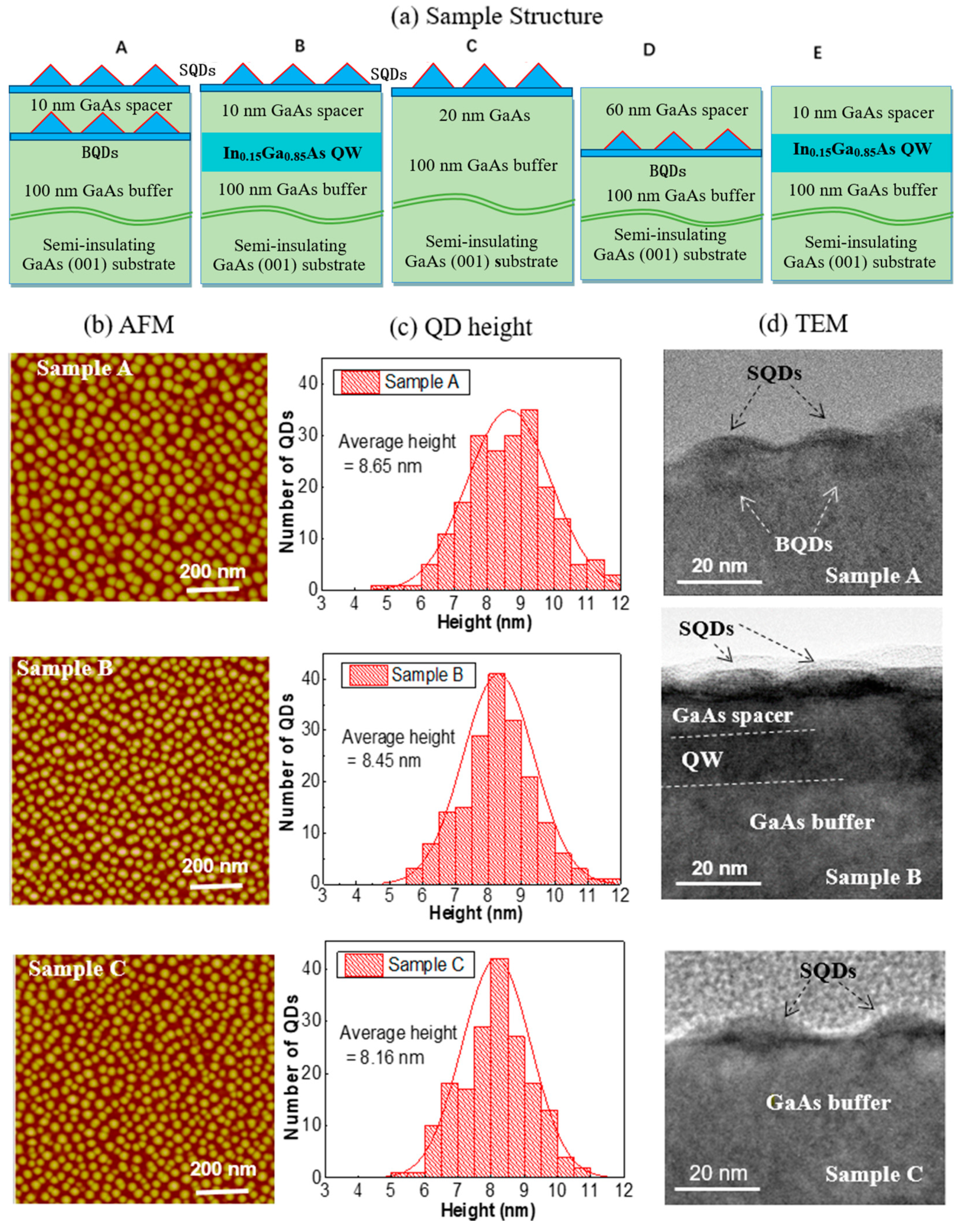
2. Materials and Methods
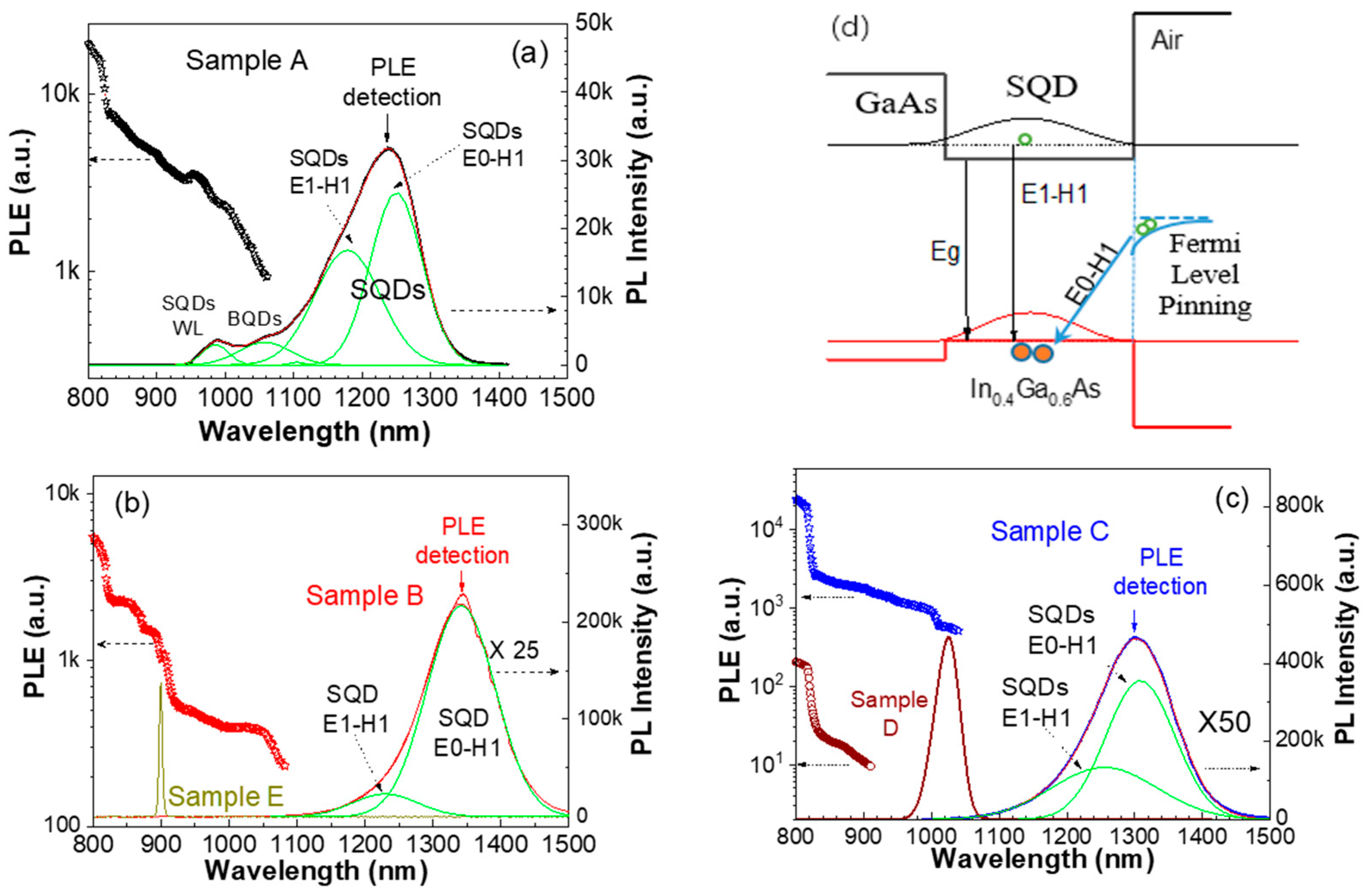
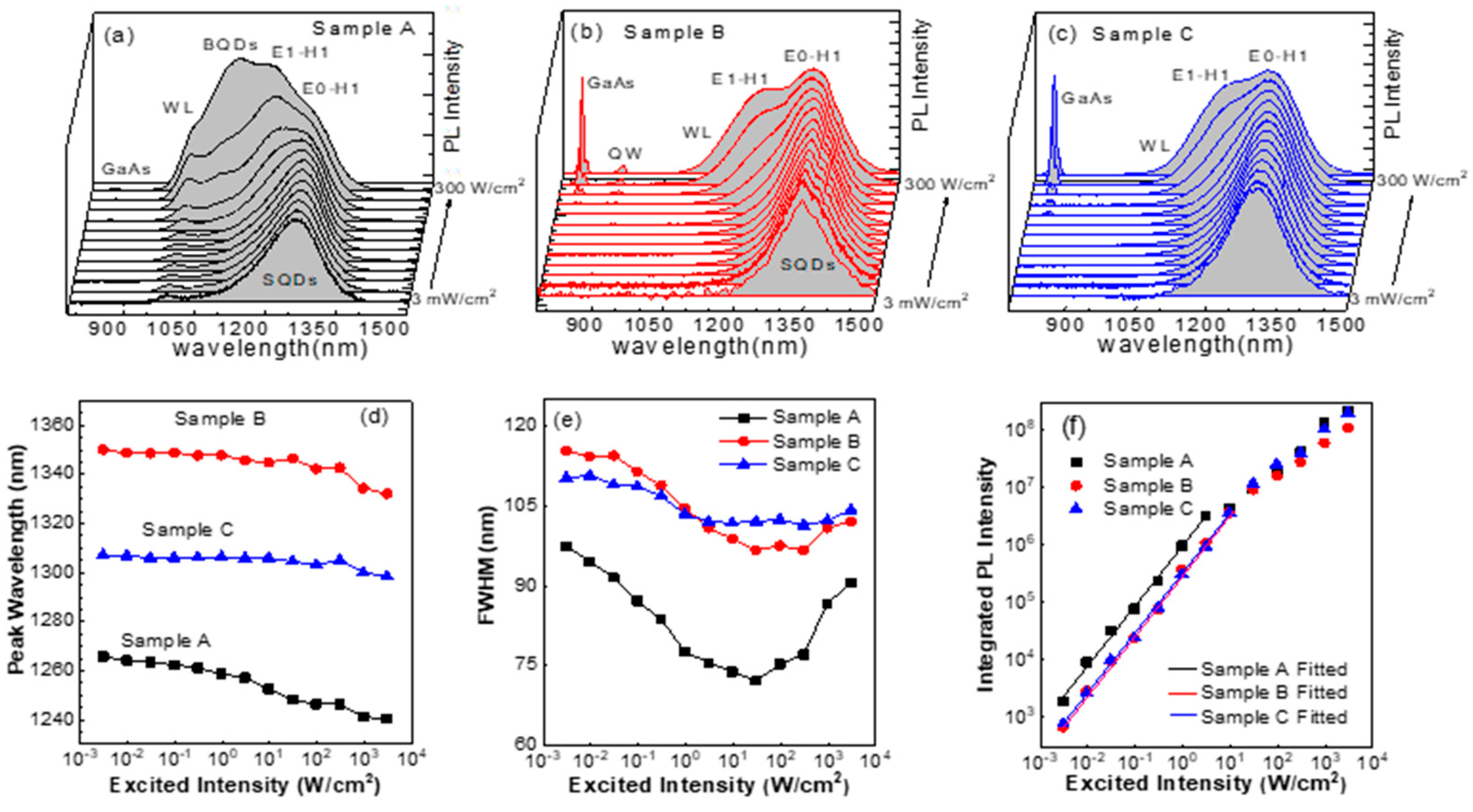
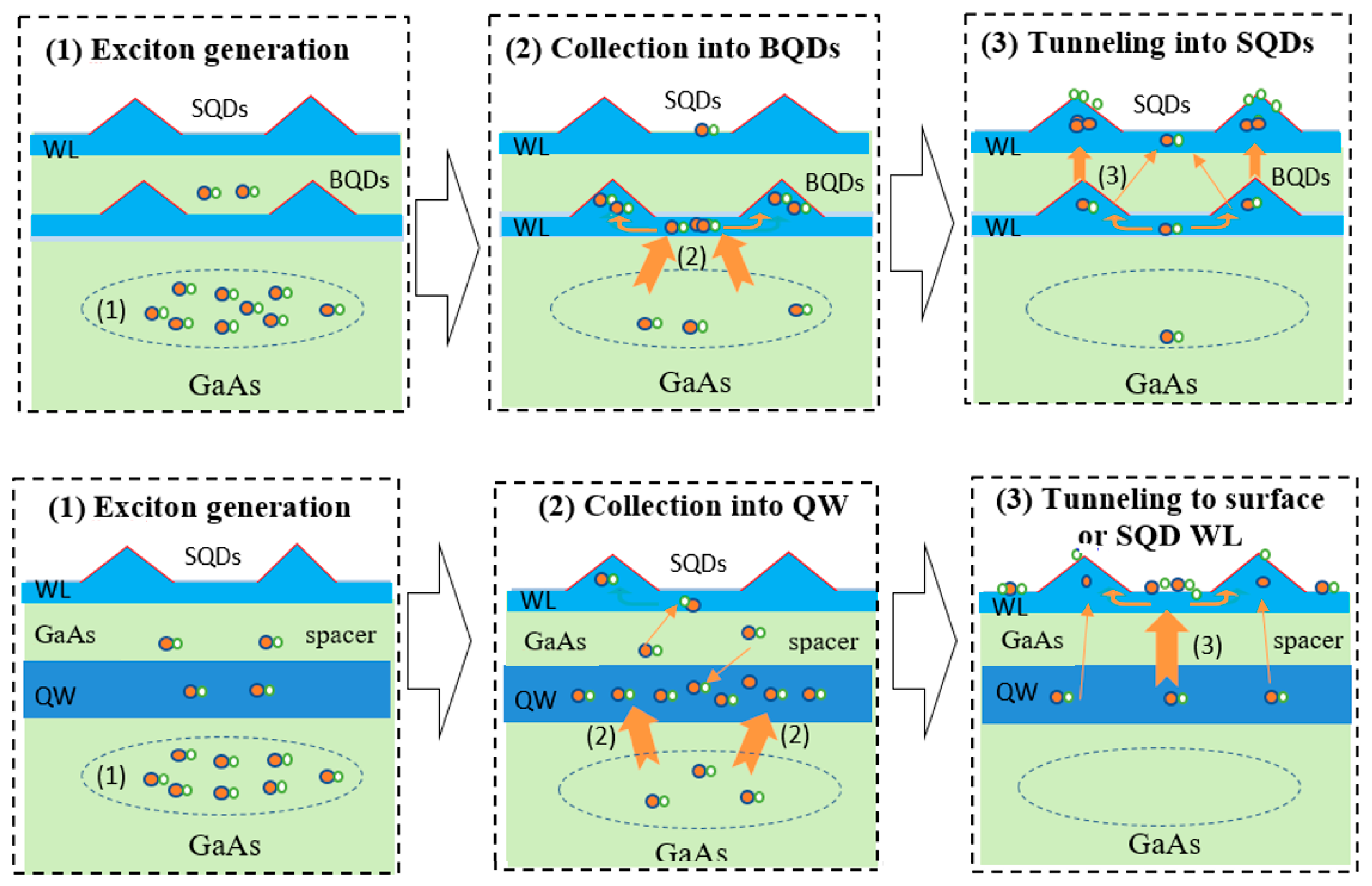
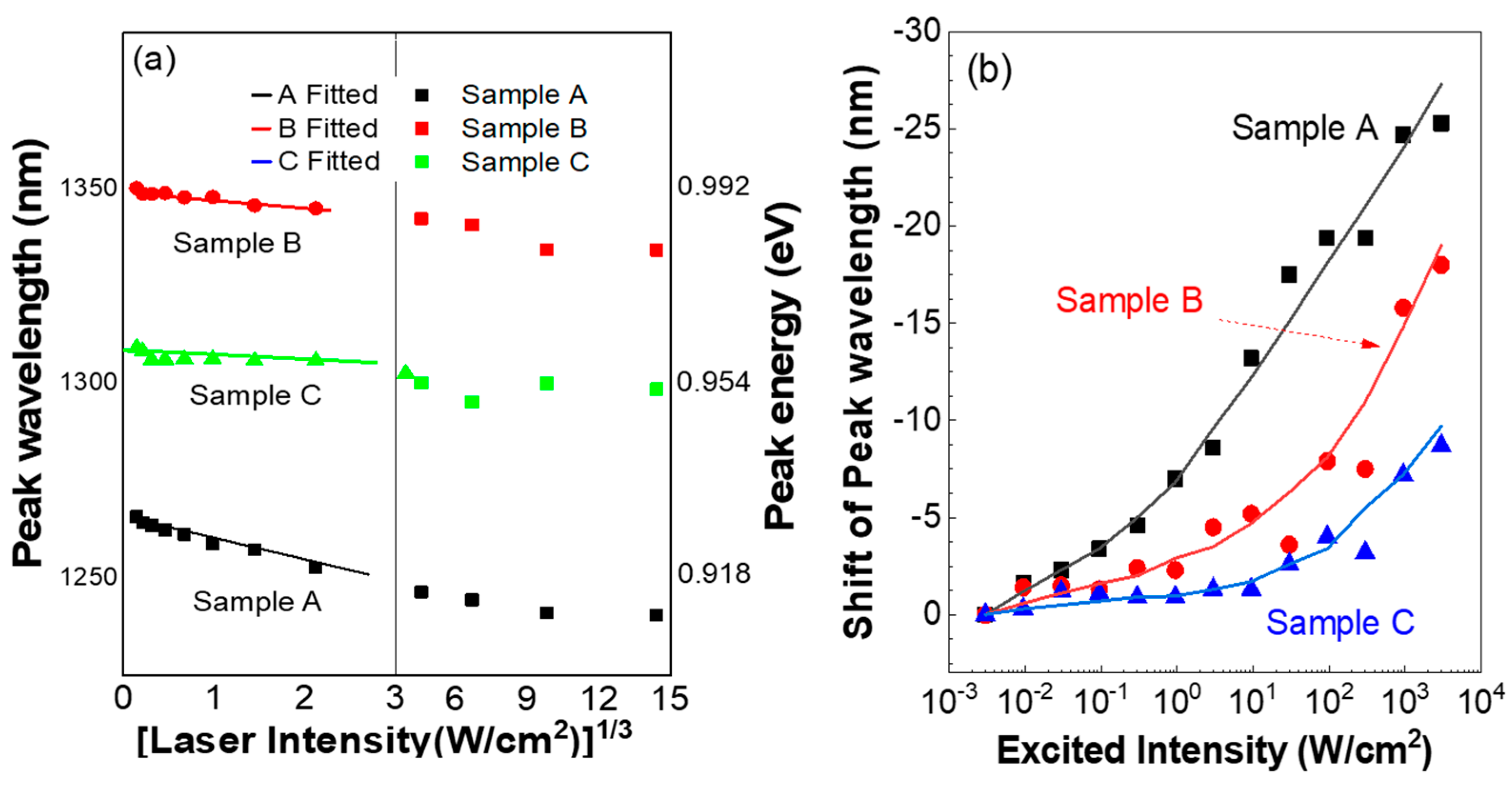
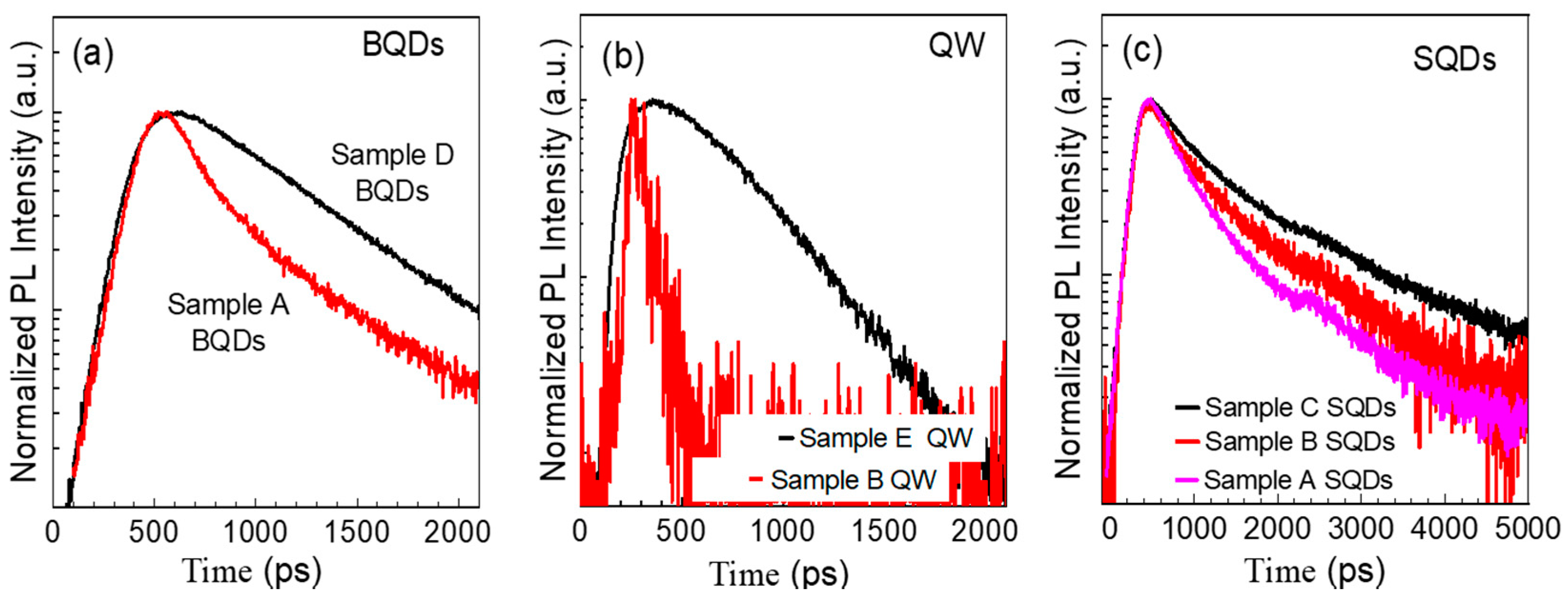
The SQD hybrid structures studied here were grown on semi-insulating GaAs (001) substrates in a VEECO Gen-930 solid-source molecular beam epitaxy (MBE) system. The sample configurations are shown schematically in Figure 1a. For sample A, after growth of a 100 nm GaAs buffer at 580 °C, 12 monolayers (MLs) of In0.4Ga0.6As were deposited to form the BQDs layer at a substrate temperature of 510 °C. Then, the 10 nm GaAs spacer was deposited. Finally 12 MLs of In0.4Ga0.6As were deposited to form the SQDs at the same substrate temperature of 510 °C. Sample B is the same as sample A, except that the BQD layer was replaced with a 12.5 nm In0.15Ga0.85As QW, deposited at 510 °C to form the injection layer. Samples C, D, and E are reference samples for the SQDs, BQDs, and the QW, respectively. Reference sample D has a GaAs capping layer of 60 nm on top of the BQDs, whereas sample E has a 10 nm GaAs capping layer on the reference QW. The 10 nm spacer thickness was selected for samples A and B to provide carrier coupling from the buried carrier injection layers to the SQDs, even though this coupling was not yet strong enough to thoroughly change the energy states of the QDs [24,25].

3. Results

Figure 1b demonstrates the morphology of the InGaAs SQDs for each sample by atomic force microscopy (AFM). Figure 1c shows the QD height distributions extracted from the respective AFM images. The areal densities of all SQD samples were measured to be ~3.0 × 1010 cm−2, while the average QD height was ~8.4 nm. All SQDs are found to be uniform and consistent; however, the SQDs in sample A are slightly larger than those in sample B, which are slightly larger than those in sample C. Strain induced from lower layers is the likely cause of this [26,27,28]. The BQDs would induce slight variations in the surface strain directly over each QD, which is averaged generally over the entire surface. This slight strain would allow for earlier nucleation of the QDs on the surface, thus allowing them to grow larger over the same time as the other samples. The strain from the QW would likely be less than that from the QD layer, but not zero, while there would be no strain before the SQD growth for reference sample C. Therefore, the SQDs in sample B should be smaller than in sample A, while those in sample C should be the smallest.
Transmission electron microscopy (TEM) in cross-section is shown in Figure 1d for each sample. The above-mentioned strain transfer can be seen in sample A by the vertical alignment of the SQDs with the BQDs [25,27]. This generally leads to efficient carrier tunneling between QDs from the buried layer to the surface layer [19], because the real distance from the BQD to the SQD inside each pair is less than 10 nm. However, sample B has a true 10 nm GaAs spacer layer between the QW and the SQDs. Therefore, in regard to both structural (strain) and electronic coupling, sample B should have carrier injection and carrier dynamics different from sample A.
Spectroscopic measurements are very useful to reveal carrier injection and carrier dynamics in coupled QD structures. For photoluminescence (PL) measurements, the samples were mounted in a variable temperature cryostat and excited by a continuous-wave laser working at a 532 nm wavelength. A 20× objective lens was used to both focus the laser beam on the sample surface and collect the PL signal. The PL signal was then sent onto the entrance slit of a 50 cm diffractive spectrometer that connected with a liquid nitrogen-cooled, charge-coupled device (CCD) as the detector. For the PL excitation (PLE) and time-resolved photoluminescence (TRPL) measurements, the laser excitation was changed to a NKT Supercontinuum pulse laser.
Figure 2a–c show the PL spectra taken at 10 K using 3 W/cm2 laser light excitation. The PL spectra of the reference samples help to clarify the assignment of the emission signals in the other samples. In Figure 2c, the reference sample C has one broad PL peak at ~1300 nm (~0.953 eV), with a linewidth (full width at the half maximum, FWHM) of ~140 nm from the SQDs emission, while reference sample D exhibits one prominent emission peak for the BQDs at ~1020 nm (~1.215 eV), with a linewidth of ~41 nm. The QW reference in sample E (Figure 2b) shows a narrow peak at 910 nm (~1.36 eV), with a FWHM of ~4.5 nm. In comparison with the single-peak spectrum of reference samples C and D, three prominent PL peaks appear for sample A in Figure 2a. Here, the long wavelength peak at ~1250 nm is attributed to the SQDs emission, the middle wavelength peak at ~1064 nm to the BQDs, and the short wavelength band at ~998 nm to the SQD wetting layer (WL) [12,19]. However, for sample B in Figure 2b, there is no emission observed from the QW, while only one broad PL peak is found at ~1320 nm from SQDs. The absence of the QW signal in sample B and the loss of BQD intensity in sample A demonstrate that there is strong coupling and carrier transfer from the buried structures to the SQDs in both samples A and B. For all three SQD samples, the SQD emissions exhibit asymmetric spectral profiles. Two peaks are extracted and are assigned to the indirect transition (E0-H1) and the direct transition (E1-H1) in the SQDs. As indicated by the band diagram in Figure 2d, the SQDs exhibit carrier separation due to Fermi-level pinning, where electrons are pinned at the surface (E0), but holes are confined within the SQDs (H1) [29].
Details of the carrier transfer into the SQDs were obtained through PLE measurements at 10 K, detecting at the SQD PL maxima for samples A, B, and C, and at the BQDs PL maximum for sample D. These are shown in Figure 2, respectively. Here, it can be seen that the GaAs matrix exhibits its well-known response at ~820 nm for all samples [30]. At the same time, reference sample D exhibits an absorption band between 820 and 870 nm due to the wetting layer (WL) absorption of the buried InGaAs QDs [31]. The SQD reference sample C has an enhanced absorption band extending to ~1000 nm due to the SQD WL [12]. Finally, we see that both samples A and B show more complicated PLE spectra than the reference samples. Sample B has a step-like PLE spectrum, in which distinct absorption band edges can be seen at ~1000 nm and ~910 nm, representing the WL of SQDs and the QW, respectively. So, there is a pathway for carrier tunneling from the QW into SQDs in sample B. For sample A, the PLE spectrum shows a broad, ramp-like absorption band spreading from 820 nm to ~1000 nm, which is the absorption band edge of SQD WL. This broad band likely consists of two sub-bands at 860–890 nm and 930–980 nm, respectively. In consideration of the BQD PLE from sample D and our previous study, we conclude that the sub-band at 860–890 nm is likely derived from the BQD WL [19], while the sub-band at 930–990 nm is likely correlated with the carrier transferring directly from BQDs to SQDs. However, in this ramp-like PLE spectrum, it is hard to clearly distinguish the sub-bands and their originations, indicating that hybrid electronic states are possibly formed in sample A due to the vertical alignment and quantum coupling between the paired BQDs and SQDs [32,33]. The hybrid electronic states can provide efficient channels for carrier transfer directly from BQDs to SQDs.
Excitation intensity-dependent PL was then performed at 10 K. The intensity-normalized PL spectra of samples A, B, and C are shown in Figure 3a–c, respectively, in which the SQDs exhibit band-filling properties in all three samples. With increasing excitation intensity, the SQDs exhibit a state-filling-like sequence of emission peaks appearing at increasing energy from the SQD E0-H1, SQD E1-H1, and SQD WL, which were each fit with Gaussians for analysis. For the coupled structures under strong excitation intensity, we also observe that the BQD peak becomes dominant in the spectrum of sample A in Figure 3a, and the QW signal appears for sample B in Figure 3b. At the highest intensities, the GaAs emission is observed at 825 nm for all three samples.
We extracted the PL peak wavelength in Figure 3d, FWHM in Figure 3e, and integrated PL intensity in Figure 3f for the SQD E0-H1 emission peak. Figure 3d,e demonstrate two regimes in the excitation intensity dependence. The peak wavelength for each sample blue-shifts, and the PL FWHM decreases as the excitation intensity increases from 3 mW/cm2 to ~10 W/cm2. The blue shift of the peak is 14.5 nm, 6 nm, and 3 nm, respectively, while the FWHM reduces by 17 nm, 14.5 nm, and 8.6 nm for samples A, B, and C, respectively. In the second regime, with an excitation intensity stronger than 10 W/cm2, the peak energy shift accelerates, while the FWHM also increases rapidly. This is due to a saturation of the E0-H1 emission, as well as an enhancement of the E1-H1 recombination of SQDs, and this is confirmed by the PL spectra variation in Figure 3a–c. The two regimes for the blue shift of SQD PL peak indicated the mechanisms to be “band bending” and “state-filling”, resulting from the indirect transition for the SQDs [29,34]. It is also worth noting that the three samples reached minima in the FWHM at different excitation intensities. This indicates that, under the same excitation intensity, the SQDs have different carrier collection or emission efficiencies in these three samples, even though they have the same SQD density.
Figure 3f shows the integrated PL intensity of the SQDs for these three samples as functions of the laser excitation intensity. A power law fit to the PL intensity as a function of the excitation intensity (3 mW/cm2 to ~10 W/cm2), P, given by, IPL = η Pα, reveals the recombination mechanisms here [14,35]. The parameters α and η are determined by fitting. The values for α are found to be 1.052, 1.042, and 1.116 for samples A, B, and C, respectively, which are all nearly equal to unity. This indicates that exciton recombination is primarily responsible for all SQD E0-H1 emissions [35]. However, the values for η, which indicate the efficiency of the PL, are more varied. For sample A, we find η = 1.008 × 10⁶, but for samples B and C, η = 3.552 × 10⁵ and 2.718 × 10⁵, respectively. Clearly, the density of carriers involved in radiative recombination in sample A is much higher than in samples B or C. This indicates that the BQD layer in sample A effectively collects carriers then injects them into the SQDs. Surprisingly, sample B appears to have a similar PL efficiency to the SQDs in the reference sample, even though sample B has a QW injection layer feeding it. In general, the InGaAs QW should capture more carriers than a single layer of BQDs due to the larger volume of QW. Therefore, more carriers should be injected from the QW into the SQDs in comparison with the BQDs injecting into the SQDs in sample A. However, the results in Figure 3f reveal that the QW-injected SQD structure may contradict the traditional QW-injected BQD structures, which have been demonstrated to be very efficient for improving the device performance of QD lasers and detectors [36,37,38].
This reduced carrier injection from the QW into the SQDs can likely be attributed to several different mechanisms. First, the TEM in Figure 1d confirms that the barrier thickness from the BQDs to the vertically-aligned SQDs in sample A is much smaller than the distance from the QW to the SQDs in sample B [19,39]. Therefore, the probability for carrier tunnel transfer from the BQDs to the SQDs is much higher than that from the QW to SQDs. Second, hybrid energy states are likely formed due to the strong coupling between the vertically aligned BQDs and SQDs in sample A. Carriers collected by the BQDs in sample A are efficiently transferred into SQDs through these hybrid states, as indicated by the diagram in Figure 4. In comparison, carriers collected by the QW in sample B cannot efficiently inject into SQDs through a suitable channel, other than tunneling through the 10 nm GaAs spacer. Third, many of the carriers supplied from the QW are not injected into the SQDs but into the SQD WL, where they mostly recombine non-radiatively through surface states rather than relax into the SQDs. In comparison, in sample A, the BQDs have a lower ground energy state than the SQD WL, so the carriers inside the BQDs cannot tunnel into the SQD WL. Instead, they tunnel into the SQDs directly.
The above results indicate that samples A and B have different carrier dynamics for transfer and recombination. Figure 4 shows schematically the carrier dynamics in samples A and B, including: (1) exciton generation inside the GaAs matrix, (2) relaxation into the BQDs or the QW, and finally, (3) tunneling into the SQDs or into the SQD WL and loss to the surface. As shown by the schematic, with the 532 nm laser excitation, in both samples A and B, most of the photo-generated carriers were generated inside the GaAs matrix, due to its large and effective volume relative to the QW or QDs. The photo-generated carriers relax into the BQDs in sample A, then transfer into SQDs, and finally recombine inside the SQDs. However, in sample B, most of the carriers relax into the QW and then transfer into the WL of the SQDs to be lost to surface states via non-radiative recombination. Therefore, the QW as an injection source for SQDs may not work well in contrast to the well-known efficient QW injection seen for buried structures.
In addition, we have previously shown that the InGaAs SQDs have recombination via spatially-indirect transitions [29]. These result from the electrons in the SQDs being accumulated in the surface states due to Femi-level pinning, while the holes remain inside the SQDs, leading to charge separation and band bending for the SQDs. Therefore, as additional evidence, the PL peak energy of the SQDs for the three samples should linearly depend on the cube root of the excitation laser intensity [40,41]. This can be recognized by:
EPL = E0PL + k P1/3
where P is the excitation intensity, E0PL is the PL-peak position at zero laser power, and k ∝ n2/3PL depends on the accumulated carrier density. Figure 5a shows the results of fitting Equation (1) to the peak wavelength (peak energy) of the SQD E0-H1 emission for the three samples. The coefficient, k, is extracted and found to be 0.00642, 0.00199, and 0.00077 for samples A, B, and C, respectively. It can be seen that the k in sample A is almost triple that of sample B. This again demonstrates that more carriers are injected into the SQDs in sample A than in sample B. In addition, Figure 5b confirms this by plotting the shift of the SQD E0-H1 emission as a function of the excitation intensity, where the SQDs in sample A have a much faster, larger PL peak wavelength shift than that of sample B.
Finally, TRPL was measured at 10 K to explore the effect of the carrier injection from the BQDs or the QW into the SQDs. The TRPL spectra, which were excited with a Supercontinuum laser (operated at 532 nm, repetition Rate ~78 MHz, and pulse width ~16 ps), were measured by a PicoHarp-300 time-correlated-single-photon-counting (TCSPC) system, combined with either a fast NIR-PMT (Hamamatsu, H10330B-75) or a SPAM (PicoQuant, SPD-100-CTC-FC) detector to match with the SQDs or QW emission signal. The TRPL signals were measured at the peak wavelength of the QW, BQDs, and SQDs emission for each sample. As plotted in Figure 6, mono-exponential decay curves are found for the reference BQDs, which were fitted using the function I(t) = A1exp[−(t−t0)/τ1]. In comparison, the decay curves for the SQDs were determined to be multi-exponential in nature, and the bi-exponential function, I(t) = A1 exp[−(t−t0)/τ1] + A2 exp[−(t−t0)/τ2], was used to fit them. This was due to either the indirect transition of the SQDs or the fast carrier transfer from the SQDs to surface states [42,43]. In this case, we associate the index, 1, with the slower lifetime of carrier recombination, τ1, and the index, 2, with the faster carrier transfer time, τ2, from the SQDs to the surface states. The amplitudes, A1 and A2, give the magnitude of the contribution from each process.
For the reference samples, the BQDs, QW, and the SQDs in Figure 6 are found to have lifetimes of 1.06 ns, 0.32 ns, and 1.58 ns, respectively. For the coupled structures, as shown in Figure 6c, the SQDs are determined to have lifetimes of 1.68 ns for sample A and 1.8 ns for sample B. It can be seen that the lifetimes of the SQDs for the three samples are similar, indicating that the injection of carriers does not have a significant impact on carrier lifetime of the SQDs. However, the lifetime of the BQDs, 0.32 ns in sample A, and from the QW, 0.11 ns in sample B, is quite different from the reference BQDs, 1.06 ns in sample D, and the reference QW, 0.32 ns in sample E. Therefore, in the coupled hybrid structures, carrier transfer is in strong competition with the radiative recombination. Using a simple model treating the hybrid structure as a three-energy-level system, the measured PL decay time for the reservoir layer is given by τPL = τs × τt/(τs + τt), where τPL is the measured lifetime for QW or BQDs in the hybrid structures, and τt is the carrier tunneling time from the carrier reservoir to the SQDs [36,39]. From the TRPL data in Figure 6, we find that the carrier tunneling time from BQDs to SQDs is about 0.16 ns, while it is 0.46 ns from QW to SQDs. Here, the much longer carrier tunneling time is from the QW to SQDs, supporting the lower emission efficiency for the SQDs in sample B. This indicates that the carrier injection from the QW is dominated by carrier tunneling from the QW to the WL of SQDs, and then transferring to the surface states, but not to the SQDs. It also should be mentioned that different rise times are found in Figure 6, between the QW and the SQD emission. This is due to the different response time of the PMT and SPAM photodetectors.

4. Conclusions

We conducted a comparative study for two hybrid SQD structures: one with a layer of InGaAs BQDs and one with an InGaAs QW to inject carriers into the SQDs. The carrier injection dynamics from the BQDs or QW to the SQDs were investigated by spectroscopic measurements. The PL, PLE, and TRPL results indicated that carrier capture and emission efficiency of the SQDs in the bilayer QD structure were stronger than those of the QW injection structure. In both samples, most of the photo-generated carriers were generated inside the GaAs layer. The photo-generated carriers relax into the BQDs and then efficiently inject into the SQDs, and finally recombine inside the SQDs. However, in the QW-injected structure, after the carriers were collected by the QW, they were transferred mostly to the WL of the SQDs, and finally, were lost to surface states via non-radiative recombination. These observations demonstrate different carrier dynamics, including carrier generation, relaxation, transfer, and recombination in the two different hybrid SQD structures. Finally, it is concluded that QD injection is better than the QW injection for SQD hybrid structures.

Author Contributions

Data curation, S.L.; funding acquisition, S.W.; investigation, J.L. and X.L.; methodology, Y.W. and C.W.; supervision, G.F. and G.J.S.; validation, S.W.; writing—original draft, J.L.; writing—review and editing, Y.I.M., M.E.W., and B.L. All authors have read and agreed to the published version of the manuscript.

Funding

The authors acknowledge the support from the Natural Science Foundation of Hebei Province (F2019201446), the Advanced Talents Incubation Program of Hebei University (8012605), and the National Natural Science Foundation of China (61774053).

Institutional Review Board Statement

Not applicable.

Informed Consent Statement

Not applicable.

Data Availability Statement

All data that support the findings of this study are included within the article.

Conflicts of Interest

The authors declare no conflict of interest.

References

  1. Leonard, D.; Krishnamurthy, M.; Reaves, C.M.; Denbaars, S.P.; Petroff, P.M. Direct formation of quantum-sized dots from uniform coherent islands of InGaAs on GaAs surfaces. Appl. Phys. Lett. 1993, 63, 3203–3205. [Google Scholar] [CrossRef]
  2. Bhattacharya, P.; Ghosh, S.; Stiff-Roberts, A.D. Quantum dot opto-electronic devices. Annu. Rev. Mater. Sci. 2004, 34, 1–40. [Google Scholar] [CrossRef]
  3. Chuang, K.Y.; Tzeng, T.E.; Lay, T.S. Coupled InGaAs Quantum Dots for Electro-Optic Modulation. Crystals 2021, 11, 1159. [Google Scholar] [CrossRef]
  4. Shang, X.J.; Li, S.L.; Liu, H.Q.; Ma, B.; Su, X.B.; Chen, Y.; Shen, J.X.; Hao, H.M.; Liu, B.; Dou, X.M.; et al. Symmetric Excitons in an (001)-Based InAs/GaAs Quantum Dot Near Si Dopant for Photon-Pair Entanglement. Crystals 2021, 11, 1194. [Google Scholar] [CrossRef]
  5. Ferdos, F.; Wang, S.M.; Wei, Y.Q.; Larsson, A.; Sadeghi, M.; Zhao, Q.X. Influence of a thin GaAs cap layer on structural and optical properties of InAs quantum dots. Appl. Phys. Lett. 2002, 81, 1195–1197. [Google Scholar] [CrossRef]
  6. Jin, P.; Meng, X.Q.; Zhang, Z.Y.; Li, C.M.; Xu, B.; Liu, F.Q.; Wang, Z.G.; Li, Y.G.; Zhang, C.Z.; Pan, S.H. Effect of InAs quantum dots on the Fermi level pinning of undoped-n+ type GaAs surface studied by contactless electroreflectance. J. Appl. Phys. 2003, 93, 4169–4172. [Google Scholar] [CrossRef]
  7. Duijs, E.F.; Findeis, F.; Deutschmann, R.A.; Bichler, M.; Zrenner, A.; Abstreiter, G.; Adlkofer, K.; Tanaka, M.; Sackmann, E. Influence of Thiol Coupling on Photoluminescence of Near Surface InAs Quantum Dots. Phys. Status Solidi B 2001, 224, 871–875. [Google Scholar] [CrossRef]
  8. Jin, P.; Meng, X.Q.; Zhang, Z.Y.; Li, C.M.; Qu, S.C.; Xu, B.; Liu, F.Q.; Wang, Z.G.; Li, Y.G.; Zhang, C.Z.; et al. Modulation Spectroscopy of GaAs Covered by InAs Quantum Dots. Chin. Phys. Lett. 2002, 19, 1010–1012. [Google Scholar]
  9. Chen, M.X.; Kobashi, K. Probing into hybrid organic-molecule and InAs quantum-dots nanosystem with multistacked dots-in-a-well units. J. Appl. Phys. 2012, 112, 064903. [Google Scholar] [CrossRef]
  10. Milla, M.J.; Ulloa, J.M.; Guzmán, Á. Strong Influence of the Humidity on the Electrical Properties of InGaAs Surface Quantum Dots. ACS Appl. Mater. Interfaces 2014, 6, 6191–6195. [Google Scholar] [CrossRef]
  11. Trevisi, G.; Seravalli, L.; Frigeri, P. Photoluminescence monitoring of oxide formation and surface state passivation on InAs quantum dots exposed to water vapor. Nano Res. 2016, 9, 3018–3026. [Google Scholar] [CrossRef]
  12. Yuan, Q.; Liu, J.T.; Liang, B.L.; Ren, D.K.; Wang, Y.; Guo, Y.N.; Wang, S.F.; Fu, G.S.; Mazur, Y.I.; Ware, M.E.; et al. Lateral carrier transfer for high density InGaAs/GaAs surface quantum dots. J. Lumin. 2020, 218, 116870. [Google Scholar] [CrossRef]
  13. Milla, M.J.; Ulloa, J.M.; Guzman, A. Photoexcited induced sensitivity of InGaAs surface QDs to environment. Nanotechnology 2014, 25, 445501. [Google Scholar] [CrossRef] [PubMed] [Green Version]
  14. Yuan, Q.; Liang, B.L.; Zhou, C.; Wang, Y.; Guo, Y.N.; Wang, S.F.; Fu, G.S.; Mazur, Y.I.; Ware, M.E.; Salamo, G.J. Interplay effect of temperature and excitation intensity on the photoluminescence of InGaAs/GaAs surface quantum dots. Nanoscale Res. Lett. 2018, 13, 387. [Google Scholar] [CrossRef] [PubMed]
  15. Wang, G.D.; Liang, B.L.; Juang, B.C.; Das, A.; Debnath, M.C.; Huffaker, D.L.; Mazur, Y.I.; Ware, M.E.; Salamo, G.J. Comparative study of photoluminescence from In0.3Ga0.7As/GaAs surface and buried quantum dots. Nanotechnology 2016, 27, 465701. [Google Scholar] [CrossRef]
  16. Wang, G.D.; Ji, H.Q.; Shen, J.L.; Xu, Y.H.; Liu, X.L.; Fu, Z.Y. Strong Influence of Temperature and Vacuum on the Photoluminescence of In0.3Ga0.7As Buried and Surface Quantum Dots. Photonic Sens. 2018, 8, 213–219. [Google Scholar] [CrossRef]
  17. Wang, G.D.; Liu, Z.G.; Wang, J.J.; Yang, Y.L.; Liu, X.L.; Zhang, X.R.; Zhang, L.W.; Cao, G.H. Gas Sensitivity of In0.3Ga0.7 As Surface QDs Coupled to Multilayer Buried QDs. Photonic Sens. 2020, 10, 283–290. [Google Scholar] [CrossRef] [Green Version]
  18. Liang, B.L.; Wang, Z.M.; Mazur, Y.I.; Salamo, G.J. Photoluminescence of surface InAs quantum dot stacking on multilayer buried quantum dots. Appl. Phys. Lett. 2006, 89, 243124. [Google Scholar] [CrossRef]
  19. Liu, J.T.; Yuan, Q.; Liang, B.L.; Yan, Q.G.; Wang, Y.; Wang, C.S.; Wang, S.F.; Fu, G.S.; Mazur, Y.I.; Ware, M.E.; et al. Photoluminescence characterization of wetting layer and carrier dynamics for coupled InGaAs/GaAs surface quantum dot pair structures. Opt. Express 2020, 28, 20704–20713. [Google Scholar] [CrossRef]
  20. Walter, G.; Chung, T.; Holonyak, N., Jr. High-gain coupled InGaAs quantum well InAs quantum dot AlGaAs–GaAs–InGaAs–InAs heterostructure diode laser operation. Appl. Phys. Lett. 2002, 80, 1126–1128. [Google Scholar] [CrossRef]
  21. Rudno-Rudziński, W.; Sęk, G.; Ryczko, K.; Syperek, M.; Misiewicz, J.; Semenova, E.S.; Lemaitre, A.; Ramdane, A. Room temperature free carrier tunneling in dilute nitride based quantum well -quantum dot tunnel injection system for 1.3 m. Appl. Phys. Lett. 2009, 94, 171906. [Google Scholar] [CrossRef]
  22. Walter, G.; Holonyak, N., Jr.; Ryou, J.H.; Dupuis, R.D. Coupled InP quantum-dot InGaP quantum well InP–InGaP–In(AlGa)P–InAlP heterostructure diode laser operation. Appl. Phys. Lett. 2001, 79, 3215–3217. [Google Scholar] [CrossRef]
  23. Amtout, A.; Raghavan, S.; Rotella, P.; Von Winckel, G.; Stintz, A.; Krishna, S. Theoretical modeling and experimental characterization of InAs/InGaAs quantum dots in a well detector. J. Appl. Phys. 2004, 96, 3782–3784. [Google Scholar] [CrossRef]
  24. Persano, A.; Cola, A.; Taurino, A.; Catalano, M.; Lomascolo, M.; Convertino, A.; Leo, G.; Cerri, L.; Vasanelli, A.; Vasanelli, L. Electronic structure of double stacked InAs/GaAs quantum dots: Experiment and theory. J. Appl. Phys. 2007, 101, 094314. [Google Scholar] [CrossRef]
  25. Talalaev, V.G.; Tomm, J.W.; Zakharov, N.D.; Werner, P.; Novikov, B.V.; Tonkikh, A.A. Transient spectroscopy of InAs quantum dot molecules. Appl. Phys. Lett. 2004, 85, 284–286. [Google Scholar] [CrossRef] [Green Version]
  26. Howe, P.; Abbey, B.; Le Ru, E.C.; Murray, R.; Jones, T.S. Strain-interactions between InAs/GaAs quantum dot layers. Thin Solid Film. 2004, 464–465, 225–228. [Google Scholar] [CrossRef]
  27. Xie, Q.; Madhukar, A.; Chen, P.; Kobayashi, N.P. Vertically self-organized InAs quantum box islands on GaAs (100). Phys. Rev. Lett. 1995, 75, 2542–2545. [Google Scholar] [CrossRef]
  28. Alonso-Álvarez, D.; Alén, B.; Ripalda, J.M.; Rivera, A.; Taboada, A.G.; Llorens, J.M.; González, Y.; González, L.; Briones, F. Strain driven migration of In during the growth of InAs/GaAs quantum posts. APL Mater. 2013, 1, 022112. [Google Scholar] [CrossRef] [Green Version]
  29. Liu, X.H.; Liu, J.T.; Liang, B.L.; Wang, Y.; Wang, S.F.; Fu, G.S.; Mazur, Y.I.; Maidaniuk, Y.; Ware, M.E.; Salamo, G.J. Type-II characteristics of photoluminescence from InGaAs/GaAs surface quantum dots due to Fermi level pinning effect. Appl. Surf. Sci. 2022, 578, 152066. [Google Scholar] [CrossRef]
  30. Mazur, Y.I.; Dorogan, V.G.; Guzun, D.; Marega, E., Jr.; Salamo, G.J.; Tarasov, G.G.; Govorov, A.O.; Vasa, P.; Lienau, C. Measurement of coherent tunneling between InGaAs quantum wells and InAs quantum dots using photoluminescence spectroscopy. Phys. Rev. B 2010, 82, 155413. [Google Scholar] [CrossRef]
  31. Mazur, Y.I.; Dorogan, V.G.; Marega, E., Jr.; Benamara, M.; Zhuchenko, Z.Y.; Tarasov, G.G.; Lienau, C.; Salamo, G.J. Excited state coherent resonant electronic tunneling in quantum well-quantum dot hybrid structures. Appl. Phys. Lett. 2011, 98, 083118. [Google Scholar] [CrossRef]
  32. Syperek, M.; Andrzejewski, J.; Rudno-Rudzinski, W.; Sek, G.; Misiewicz, J.; Pavelescu, E.M.; Gilfert, C.; Reithmaier, J.P. Influence of electronic coupling on the radiative lifetime in the (In,Ga)As/GaAs quantum dot–quantum well system. Phys. Rev. B 2012, 85, 125311. [Google Scholar] [CrossRef]
  33. Sek, G.; Andrzejewski, J.; Ryczko, K.; Poloczek, P.; Misiewicz, J.; Semenova, E.S.; Lemaitre, A.; Patriarche, G.; Ramdane, A. Electronic structure properties of the In(Ga)As/GaAs quantum dot–quantum well tunnel-injection system. Semicond. Sci. Technol. 2009, 24, 085011. [Google Scholar]
  34. Klenovský, P.; Steindl, P.; Geffroy, D. Excitonic structure and pumping power dependent emission blueshift of type-II quantum dots. Sci. Rep. 2017, 7, 45568. [Google Scholar] [CrossRef] [PubMed] [Green Version]
  35. Jin, S.R.; Zheng, Y.L.; Li, A.Z. Characterization of photoluminescence intensity and efficiency of free excitons in semiconductor quantum well structures. J. Appl. Phys. 1997, 82, 3870–3873. [Google Scholar] [CrossRef]
  36. Wang, Y.; Sheng, X.Z.; Yuan, Q.; Guo, Q.L.; Wang, S.F.; Fu, G.S.; Liang, B.L.; Huffaker, D.L.; Mazur, Y.I.; Yurii, M.; et al. Carrier dynamics in hybrid nanostructure with electronic coupling from an InGaAs quantum well to InAs quantum dots. J. Lumin. 2018, 202, 20–26. [Google Scholar] [CrossRef]
  37. Zhang, X.B.; Ryou, J.H.; Dupuis, R.D.; Walter, G.; Holonyak, N., Jr. Temperature-dependent luminescence of InP quantum dots coupled with an InGaP quantum well and of InP quantum dots in a quantum well. Appl. Phys. Lett. 2005, 87, 201110. [Google Scholar] [CrossRef]
  38. Goodfellow, K.M.; Chakraborty, C.; Sowers, K.; Waduge, P.; Wanunu, M.; Krauss, T.; Driscoll, K.; Vamivakas, A.N. Distance-dependent energy transfer between CdSe/CdS quantum dots and a two dimensional semiconductor. Appl. Phys. Lett. 2016, 108, 021101. [Google Scholar] [CrossRef]
  39. Liu, Y.; Liang, B.L.; Guo, Q.L.; Wang, S.F.; Fu, G.S.; Fu, N.; Mazur, Y.I.; Ware, M.E.; Salamo, G.J. Electronic coupling in nanoscale InAs/GaAs quantum dot pairs separated by a thin Ga(Al)As spacer. Nanoscale Res. Lett. 2015, 10, 271. [Google Scholar] [CrossRef] [Green Version]
  40. Alonso-Álvarez, D.; Alén, B.; García, J.M.; Ripalda, J.M. Optical investigation of type II GaSb/GaAs self-assembled quantum dots. Appl. Phys. Lett. 2007, 91, 263103. [Google Scholar] [CrossRef] [Green Version]
  41. Chiu, Y.S.; Ya, M.H.; Su, W.S.; Chen, Y.F. Properties of photoluminescence in type-II GaAsSb/GaAs multiple quantum wells. J. Appl. Phys. 2002, 92, 5810–5813. [Google Scholar] [CrossRef]
  42. Couto, O.D.D., Jr.; de Almeida, P.T.; dos Santos, G.E.; Balanta, M.A.G.; Andriolo, H.F.; Brum, J.A.; Brasil, M.J.S.P.; Iikawa, F.; Liang, B.L.; Huffaker, D.L. Carrier dynamics dictated by bimolecular recombination in type-II quantum dots coupled to quantum wells. J. Appl. Phys. 2016, 120, 084305. [Google Scholar] [CrossRef]
  43. Liu, Y.; Wang, Y.; Liang, B.L.; Guo, Q.L.; Wang, S.F.; Fu, G.S.; Mazur, Y.I.; Ware, M.E.; Salamo, G.J. Interplay effect of excitation and temperature on carrier transfer between vertically aligned InAs/GaAs quantum dot pairs. Crystals 2016, 6, 144. [Google Scholar] [CrossRef] [Green Version]
Figure 1. Sample structures and characterizations: (a) diagram of sample structures; (b) 1 μm × 1 μm AFM images of SQDs; (c) the QD height distribution extracted from the corresponding AFM image; (d) the cross-sectional TEM images showing the SQDs with adjacent BQDs and QW structures.
Crystals 12 00319 g001
Figure 2. The PL and PLE characterization results. The PL and PLE spectra were measured at 10 K for: (a) sample A, (b) sample B and QW reference sample E, and (c) sample C and BQDs reference sample D. (d) Schematic band diagram showing the SQDs along with the surface states which result in indirect recombination.
Crystals 12 00319 g002
Figure 3. PL spectra measured at 10 K with varied excitation intensity from 3 mW/cm2 to 3000 W/cm2 for (a) sample A, (b) sample B, (c) sample C; (d) the peak wavelength, (e) the FWHM, and (f) the integrated intensity for the E0-H1 PL peak of SQDs are plotted against excitation intensity, as extracted from (ac).
Crystals 12 00319 g003
Figure 4. Demonstration of the carrier dynamics in samples A and B, including (1) exciton generation inside GaAs matrix, (2) relaxation into BQDs or QW, and finally, (3) tunneling into SQDs in sample A, or into SQD WL and then lost to the surface in sample B.
Crystals 12 00319 g004
Figure 5. (a) The PL peak wavelength (energy) as a function of the cube root of the laser excitation intensity. (b) The Shift of PL peak wavelength as a function of the laser excitation intensity.
Crystals 12 00319 g005
Figure 6. TRPL spectra measured at 10 K for (a) BQDs, (b) QW, and (c) SQDs, respectively.
Crystals 12 00319 g006
Publisher’s Note: MDPI stays neutral with regard to jurisdictional claims in published maps and institutional affiliations.

