Review

Quaternary Semiconductor Cd1−xZnxTe1−ySey for High-Resolution, Room-Temperature Gamma-Ray Detection

Department of Electrical Engineering, University of South Carolina, Columbia, SC 29208, USA
*
Author to whom correspondence should be addressed.
Crystals 2021, 11(7), 827; https://doi.org/10.3390/cryst11070827
Submission received: 30 June 2021 / Revised: 9 July 2021 / Accepted: 12 July 2021 / Published: 16 July 2021

Abstract

:
The application of Cd0.9Zn0.1Te (CZT) single crystals, the primary choice for high-resolution, room-temperature compact gamma-ray detectors in the field of medical imaging and homeland security for the past three decades, is limited by the high cost of production and maintenance due to low detector grade crystal growth yield. The recent advent of its quaternary successor, Cd0.9Zn0.1Te1−ySey (CZTS), has exhibited remarkable crystal growth yield above 90% compared to that of ~33% for CZT. The inclusion of Se in appropriate stoichiometry in the CZT matrix is responsible for reducing the concentration of sub-grain boundary (SGB) networks which greatly enhances the compositional homogeneity and growth yield. SGB networks also host defect centers responsible for charge trapping, hence their reduced concentration ensures minimized charge trapping. Indeed, CZTS single crystals have shown remarkable improvement in electron charge transport properties and energy resolution over CZT detectors. However, our studies have found that the overall charge transport in CZTS is still limited by the hole trapping. In this article, we systematically review the advances in the CZTS growth techniques, its performance as room-temperature radiation detector, and the role of defects and their passivation studies needed to improve the performance of CZTS detectors further.

1. Introduction

Penetrating radiations such as x- and γ-rays are indispensable for medical imaging through techniques such as computed tomography (CT), positron emission tomography (PET) or X-ray radiography, for security screening at the port of entries, for monitoring and safeguarding of special nuclear materials, to name a few [1,2]. At the heart of the imagers or scanners used in these applications, there is usually an x-/γ-ray detector with high spatial and energy resolution that allows direct conversion of radiation into electron-hole pairs [3,4]. For field deployability of such detectors, compact and room-temperature operation are of prime requirements. Conventional high resolution gamma-ray detectors such as HPGe and Si(Li) detectors require bulky cryogenics attachment for cooling due to their low room-temperature bandgap energies ( E g (Si) = 1.11 eV and E g (Ge) = 0.67 eV). Moreover, the photoelectric absorption coefficient for x-/γ-ray interacting with matter varies with N Z 5 where N is the density of the detecting material [5]. Hence, detector materials with a lower atomic number (Z) such as silicon ( Z S i = 14 ) imply a lower peak-to-Compton background ratio.
CdZnTe (CZT), in its prevalent stoichiometric formula for x-/γ-ray detection Cd0.9Zn0.1Te, is a wide bandgap ( E g = 1.6 eV at 300 K) ternary semiconductor which makes it perfectly suitable for room-temperature applications [6,7,8]. In addition to its high-Z constituents ( Z C d = 48 ,     Z Z n = 30 , and Z T e = 52 ) and high material density of 5.8 g/cm3, CZT also acts as an efficient γ-ray absorber where a substantial fraction of the incident radiation fully deposits its energy through photoelectric absorption. CZT also offers bulk electrical resistivity on the order of 1010 Ω-cm and even higher which results in extremely low leakage currents at high operating bias voltages [9]. Low detector leakage current in spectrometers ensures low electronic noise and high energy resolution. CZT detectors have reigned for the past three decades as direct conversion detectors at room-temperature for specialized applications in medical imaging and scanning, homeland security, nuclear non-proliferation, accounting and safeguarding of nuclear wastes, and special nuclear materials [10]. Crystal growth methods such as the travelling heater method (THM) [11,12,13] and vertical Bridgman method (VBM) [14,15,16] are the primary techniques to grow detector-grade CZT single crystals. Although large volume single crystals can be grown using THM or VBM, the crystal growth yield is generally low, meaning, only a fraction of the grown ingot is detector-grade which has the required crystallinity, homogeneity, and resistivity. Among the best reported CZT crystal growths, about one-third of the grown ingot has been found to be of detector grade quality [17]. The low crystal-growth yield enhances the cost of production of detector grade CZT crystals and results in high manufacturing cost of imagers and spectrometers based on CZT detectors.
The inhomogeneity in as-grown CZT ingots results from the crystal imperfections which in turn arise from causes inherent to the growth method. Structural defects such as sub-grain boundary networks, twin/grain boundaries and cracks, mosaic structures, tilt boundaries, dislocations, etc. are the major crystal imperfections found in CZT [6,8,18,19]. The sub-grain boundary networks host point defects such as impurities, tellurium inclusions, and antisite defects that act as potential charge trapping and recombination centers which in turn limit the radiation detection performance. Reports that emerged in the latter half of the last decade, pioneered by Brookhaven National Laboratory, established that the addition of chalcogenides such as selenium (Se) in CZT [17] subdues the sub-grain boundary networks to a substantial extent, achieving crystal growth yield exceeding 90%. The stochiometric formula Cd0.9Zn0.1Te1−ySey, commonly referred to as CZTS, with y usually ranging between 0.01 to 0.07, has since been reported by several groups to be a very high-resolution gamma-ray detector [20,21,22,23,24,25]. Although, some of the above-mentioned defects for CZT are also found in CZTS as shown in Figure 1, the recently reported energy resolution of large volume CZTS detectors is approaching the energy resolution goal of 0.5% or less for 662 keV gamma rays as set by the US Department of Energy (DOE). Both CZT and CZTS have the zinc-blende crystal structure and similar bandgap. Figure 2 shows the atomic arrangements of the constituents in a 64-atom primitive supercell. With all the pro-detection physical properties such as high-Z, high bandgap (1.6 eV), and high resistivity (> 10 10   Ω-cm) along with high crystal growth yield, CZTS has been touted as the economic alternative of CZT detectors with even better detection performance.
In this article, we review and update the advances of the CZTS detectors since its inception including crystal growth methods, detector fabrication procedures, characterization of the electrical properties, charge transport properties, radiation detection, and crystal defects that limit their performance as radiation detectors.

2. Challenges of CdZnTe Detectors

As has been mentioned above, the performance of the CZT detectors is limited by charge trapping, especially for holes. Secondary phase defects such as Te inclusions are potential hole traps and are the primary reason behind the limited energy resolution of CZT detectors. Such secondary phase Te inclusions can be restrained using post-growth annealing under Cd vapor, but it may lead to the formation of star-like defects which in turn are potential electron traps [26]. Among the typical reported values, Cd0.9Zn0.1Te single crystals exhibit drift mobilities up to 1000 (electrons) and 120 (holes) cm2V−1s−1 and mobility-lifetime (µτ) product values of 1 × 10⁻² (electrons) [27] and 1.2 × 10⁻⁴ (holes) cm2V−1 [5]. The disparately poor hole charge transport properties result in low energy resolution especially for gamma-ray detection.
Gamma rays, penetrative in nature, may interact deep inside the detector volume. Unlike charged particles, neutral gamma photons lose their entire energy abruptly at the location of interaction. On the contrary, charged particles generally lose their energy gradually along their path through the detector material until reaching their maximum range. In addition, monoenergetic gamma photons can interact at any depth unlike monoenergetic charged particles which penetrate up to a specific depth for every interaction. Thus, monoenergetic gamma rays create electron-hole charge pairs at varying depths within the detector volume for each interaction event. For high energy gamma rays, these depths can range anywhere from the detector anode to cathode, even for thick detectors. The radiation induced charge pairs are collected by applying a potential difference across the detector. The charge pairs drift towards their respective favorable polarity electrode under the influence of the applied electric field constituting a current i . With the transport properties of electrons being superior to holes, electrons are almost always collected much faster compared to holes. The charge induced on the collecting electrode ( Δ Q ) by a charge q moving from location r i to r f is a function of their distance from the collecting electrode and is given by the weighting potential   φ A given by Equation (1) [28].
Δ Q = i   d t = q [ φ A ( r i ) φ A ( r f ) ] .
A charge carrier that travels the full distance from the point of interaction to its respective electrode deposits its full charge on the electrode. If a charge carrier gets trapped while drifting towards the collecting electrode and recombines, it deposits only a portion of its charge based on how far it traveled before being trapped. Thus, the charge collected can vary widely depending on the point of trapping especially when holes are created close to the anode. The deposited charge is directly proportional to the incident radiation energy and hence carries the actual information for pulse height spectroscopy. Hence, abrupt variation in the detector output leads to uncertainty in pulse height measurement which in turn deteriorates the energy resolution. The effect of charge loss on the detector output signal has been summarized in Figure 3.
In order to compensate for the poor hole-transport properties, several device geometries have been devised which shapes the internal electric field and hence the weighting potential, resembling that of a Frisch grid detector. In a Frisch grid detector, the screening effect of the grounded Frisch grid placed between the anode and the cathode, prevents the anode from ‘seeing’ the electrons created in the neutral region by the incident radiation unless they cross the grid and step into the ‘active region’. The slower moving positive ions created in the neutral region drift towards the cathode and therefore are not ‘seen’ by the anode at all. Hence, the detector produces a signal only for the electron movement in the active region allowing it to act as a single polarity device. The working of Frisch grid has been demonstrated in Figure 3. Frisch grid effects can be enabled in large volume CZT detectors by adopting virtual Frisch grid electrode geometries such as small pixel [29,30], Frisch collar [31,32,33], coplanar grids [30,34], and drift strip electrode [35]. However, the fabrication of virtual Frisch grid geometries adds to the cost of manufacturing and often involves complicated peripheral electronics to process the signal. Had there been a scope of minimizing the hole traps, many of the above-mentioned problems associated with the CZT detectors would have disappeared. CZTS with its reduced concentration of grain boundary networks promises along the same line. Additionally, we will establish in the following sections that the probability of formation of potential electron trap centers also reduces drastically due to the presence of Se in CZTS.

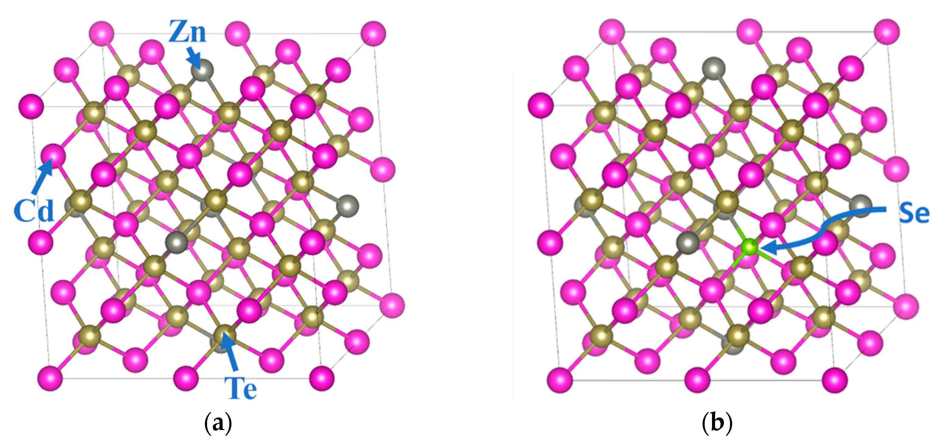
3. Role of Se in CdTe and CZT Matrix

The role of Se in the CdTe system in reducing the concentration of deep levels was demonstrated as early as 1994 by Fiederle et al. [36]. The present article focuses on the effect of Se in influencing bulk properties of Cd0.9Zn0.1Te or CdTe for detection application. For similar discussions related to thin films or other stoichiometric compositions please refer to Fiducia et al. [37] or Chanda et al. [38], respectively. Kim et al. reported in the late 2000s, the role of Se in obtaining high quality vertical Bridgman method (VBM) grown chlorine doped CdTe0.9Se0.1 (CTS) crystals which exhibited excellent axial and radial compositional uniformity throughout the ~50 mm long ingot [39]. Roy et al. reported a similar result in VBM grown CdTe0.9Se0.1 crystals without any chlorine doping [40]. The segregation coefficient of Se was found to be near unity in both reports. The segregation coefficient of an element in a quasi-molten compound is defined as the ratio of the elemental concentration in solid phase ( C s ) to that in liquid phase ( C l ), k = C s / C l . Hence, a segregation coefficient close to 1 suggests that the presence of element in both phases are similar in concentration which ensures that the element does not diffuse from the solid to the liquid phase or vice-versa, which in turn ensures compositional homogeneity of that element. The above attempts were aimed to replace Zn with Se in CZT to obtain better compositional homogeneity as k S e 1 , whereas k Z n > 1 in CdTe. The electron mobility-lifetime (µτ) product was also found to be rather high (~10−2 cm2V−1) in CTS [39,41]. The measured resistivities of the CTS crystals were reported to be in the range of 109–1010 Ω-cm [36,39,41]. The bandgap, however, was calculated to be 1.4 eV at room-temperature in CTS which is lower than that reported for CZT.
In a first, Roy et al. demonstrated the exceptional compositional homogeneity and reduced extended defects such as secondary phases and sub-grain boundary networks in CZTS grown using the travelling heater method (THM) [42,43]. Figure 4 demonstrates the compositional homogeneity obtained in their THM grown CZTS ingot. Frisch collar detectors fabricated with stoichiometry Cd0.9Zn0.1Te0.98Se0.02 exhibited an impressive energy resolution of 0.87% for 662 keV gamma rays [17]. Yakimov et al. reported the growth of Cd0.9Zn0.1Te1−xSex (with an unspecified x) using a horizontal Bridgman method, which demonstrated that the density of deep-level traps was substantially reduced, and the X-ray detection count rate was significantly increased upon inclusion of Se in CZT [23]. The reduced defect density resulted in better uniformity in the internal electric field distribution and a linear radiation response at high incident X-ray flux. In yet another work, Roy et al. demonstrated that THM grown Frisch collar CZTS detectors offered a record high energy resolution of 0.77% for 662 keV gamma rays [44]. Some of the best CZT detectors in single polarity sensing geometry are reported in the literature to offer an energy resolution of ~1% for 662 keV gamma rays [45]. In 2019, Chaudhuri et al. demonstrated robust hole signals from VBM grown Cd0.9Zn0.1Te0.97Se0.03 planar detectors which allowed them to determine and report the hole mobility and lifetime values for the first time using alpha spectroscopic techniques. The details of the carrier lifetime and mobility measurements will be presented in Section 6. It can be noticed from the above discussion that in contrast to Roy’s work, where the highest resolution mentioned was obtained for a Se concentration of 2%, Chaudhuri et al. found the best detection performance for a Se concentration of 3% in their VBM grown CZTS crystals. The concentration of Se has an apparent role in determining the CZTS device performance and will be discussed in detail in Section 9.

4. Growth Techniques of CZTS Single Crystals

Similar to CZT, the crystal growth methodology for CZTS relies on melt growth techniques such as travelling heater and Bridgman method. Both methods have their advantages and disadvantages. The concept of melt-growth process is to thermally melt high purity polycrystalline constituent elements/compounds called precursors and allow them to react enabling the synthesis of the desired compound followed by controlled re-solidification to facilitate crystallization. The solid-state reaction (synthesis) must be complete to achieve the targeted stoichiometry and that too in a homogeneous manner. The growth should be unidirectional to achieve a high degree of single-crystallinity axially and radially. The travelling heater method is a combination of zone melting and growth-from-solutions technique. In THM, a CZTS solvent zone is migrated through the solid source material while maintaining a thermal gradient which ensures the accurate cooling rate for crystallization. Detector grade large volume single crystals can be obtained using THM, however, the rate of crystal growth is typically 1–2 mm/day, which is rather slow. On the other hand, the Bridgman method and its modified versions such as VBM involve single crystal growth from a melt by progressively freezing the melt from one end to the other. The typical crystal growth rate is an order of magnitude higher (1–4 mm/h) compared to that of THM. However, crystals grown using the Bridgman method suffer from low crystal growth yield, inclusion of extended defects, and poor electron transport properties. Below are the descriptions of the methods that have been reported for the growth of detector grade CZTS.
Roy’s group used a THM growth method originally designed at Brookhaven National Laboratory [17] where they used pre-synthesized 6N (99.9999%) purity precursor materials viz., Cd0.9Zn0.1Te and CdSe. They normally add traces of indium (In) to compensate for the residual Cd vacancies that are formed in excess Te conditions [46,47]. The precursors were sealed in a quartz tube designed with a conical tip under high vacuum (10−7 Torr). The quartz tube was suspended in a three-zone furnace which was set to maintain the required thermal gradient near the growth interface. The runs were typically unseeded and hence conically tipped quartz ampoules were used to prohibit spurious nucleation centers. A low-speed high-torque DC motor actuated the ampoule for vertical motion within the furnace where typical temperature gradients in the range of 10–15 °C/cm were maintained. Typical lowering rates ranging within 3–5 mm/day were used. A slow cooling rate of 100 °C/day was used following the completion of growth runs to avoid any thermal shock.
Chaudhuri et al. used a modified VBM at the University of South Carolina (UofSC), to grow CZTS single crystals [21]. They used 7N purity elemental precursors viz., Cd, Zn, Te, and Se rather than pre-synthesized precursors. The precursors were stoichiometrically weighed with 5% excess Te and were vacuum (10−6 Torr) sealed in a conically tipped quartz tube. Excess Te helps keep the growth temperature lower and may control certain intrinsic defect levels and defect complexes in CZT by causing favorable carrier compensation [48]. No compensating agents such as In were used. The polycrystalline material was synthesized at ~1085 °C in a three-zone tubular furnace. The schematic of the furnace for a typical VBM growth is shown in Figure 5. The three separate heater controllers were programmed to achieve an axial temperature gradient of 2.5 °C/cm. In a similar arrangement as mentioned for the THM process, the ampoule tied to a quartz rod was moved downward inside the furnace at a constant velocity of 2 mm/h using a computer-controlled motor. This vertical motion cycle was repeated three times for a typical growth run which is a common practice to enhance the homogeneity and crystal growth yield. The furnace was slowly cooled following the end of run to avoid any thermal stress. The ampoule was also constantly rotated using a separate computer-controlled motor at a rotational speed of 12 rpm to maintain a uniform radial temperature distribution.
Yakimov et al. used a horizontal Bridgman method to grow single crystals of CZTS with a growth rate of 1–4 mm/h [23]. They used commercially available 6N purity CZT and 4N5 purity CdSe as precursor materials along with elemental Cd to create Cd overpressure in order to suppress the formation of Te inclusions. They have also used In doping (~3 ppm by weight) for compensation. The obtained 4 mm thick wafers contain several large grains suitable for detector fabrication.

5. CZTS Crystal Characterization and Detector Fabrication

Post growth processing of CZTS crystals is similar to that used for CZT crystals. Once the ampoule is taken out of the furnace, the quartz tube is cut open using diamond impregnated blades/saws. The ingot is carefully taken out and sliced perpendicular to the growth axis at pre-determined positions to obtain wafers. For compositional homogeneity studies, the ingots are often cut along the axis length.

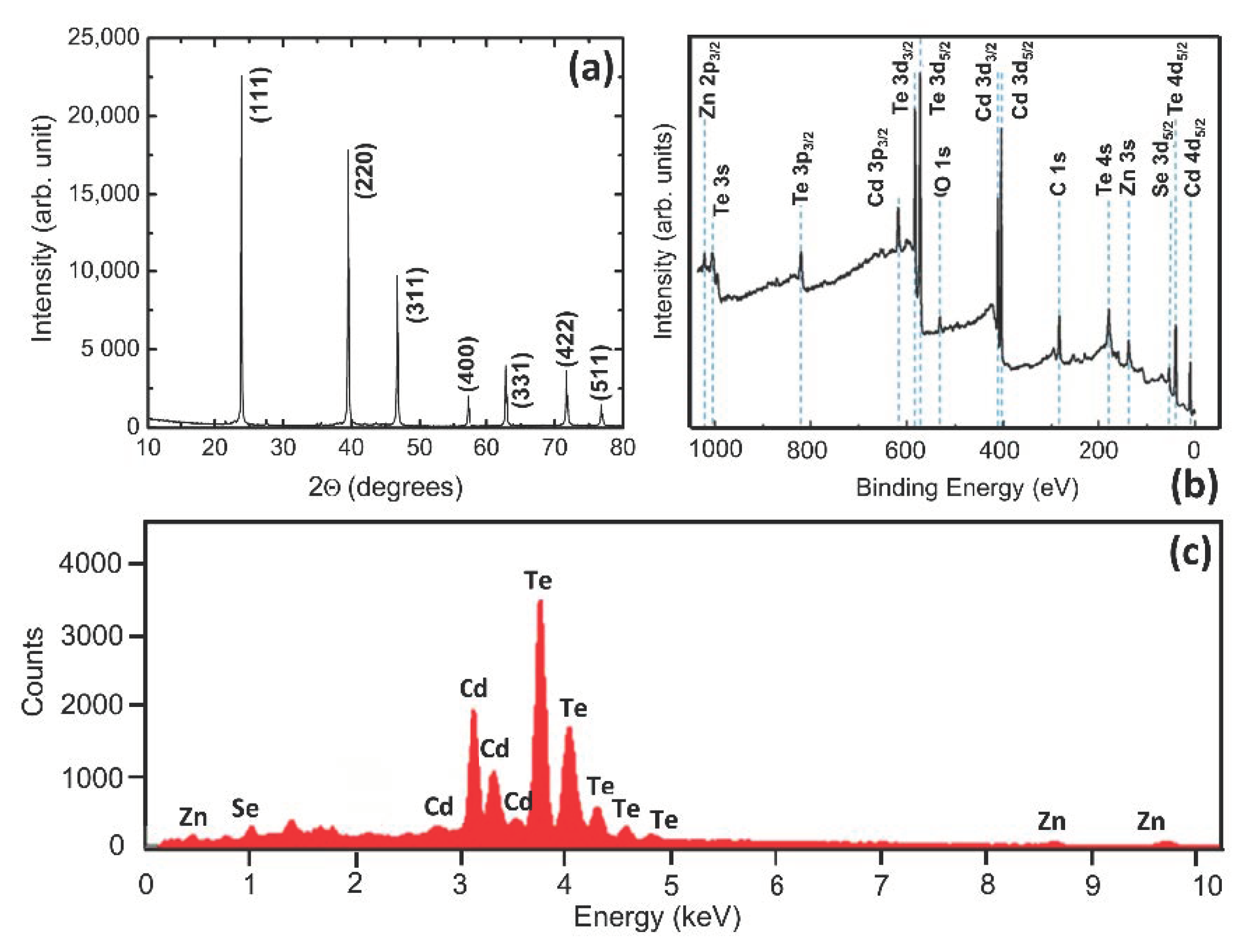
5.1. Compositional Characterization

Representative portions from grown ingot are studied to confirm the formation of the intended stoichiometry and the desired crystallinity. X-ray topography studies as mentioned in Refs. [17,23] help in understanding the homogeneity of the distribution of the elemental components such as Zn and Se (Figure 4). Powder X-ray diffraction measurements (Rigaku, Tokyo, Japan) are carried out to investigate the different crystallographic planes corresponding to the different grains present in the as-grown ingots. X-ray photoelectron spectroscopy (XPS, Kratos, Kyoto, Japan) and energy dispersive X-ray spectroscopy (EDX, TESCAN, Brno, Czech Republic) are carried out to investigate the elemental composition especially at the surface of the polished wafers. Figure 6 shows the various X-ray measurements carried out in a VBM grown CZTS crystal. The results obtained from the measurements suggested that the crystal orientations and the elemental compositions were as intended.

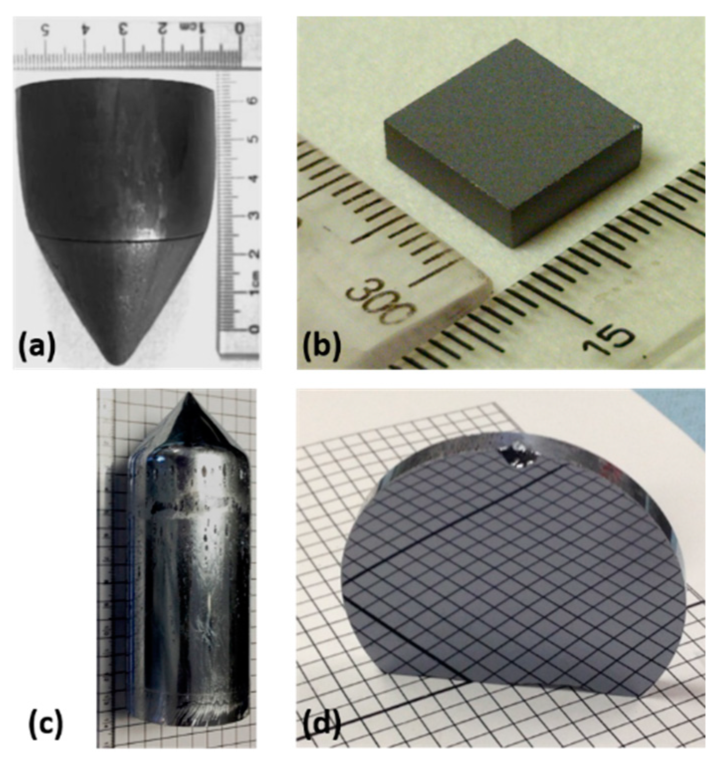
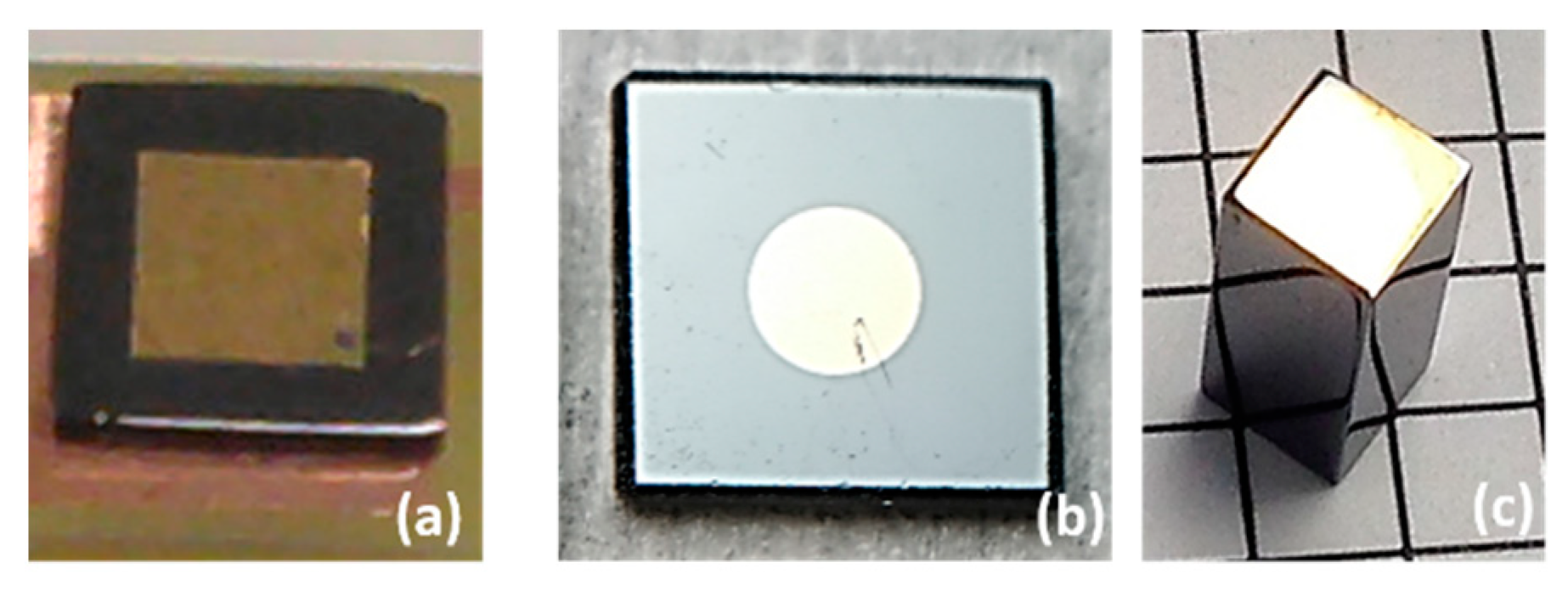
5.2. Crystal Cutting and Detector Fabrication

The grown ingots normally contain patches of single crystal regions called grains as shown in Figure 7. For detector fabrication, the wafers are visually inspected to identify the bigger grains which were cut out carefully in the form of blocks using diamond impregnated wire saws. The bigger the grain sizes are, the bigger the detector blocks could be harvested. Figure 8 shows the photographs of 2-inch diameter CZTS ingots grown using a VBM and THM method [49]. The photographs of the wafers cut out from the ingots are also shown in Figure 8. The CZTS substrates require smooth surfaces for metal deposition during detector fabrication. Any reminiscent wax used for attaching the ingots to the holders or crystal cutter chucks are cleaned using appropriate organic solvents. The wafers or blocks are first grounded and lapped mechanically starting with coarse sandpaper followed by finer grits down to 1500 grit SiC abrasive papers. The grounded wafers are then polished using an alumina powder-water slurry with grain sizes in the range 0.5 to 0.05 µm with various other sizes in between.
The lapping and polishing are generally done by hand as CZTS crystals are brittle and often of non-standard shapes and sizes to fit in standard machine chucks. The polished wafers are then thoroughly cleaned using deionized water to clean off any residual alumina powder. The cleaned wafers are chemo-mechanically polished by dipping the wafers in a 1–2% bromine-methanol (Br2-MeOH) solution for a few minutes (typically 1 min for a 2% Br2-MeOH solution) to minimize the surface defects caused by crystal cutting and polishing [50]. The chemo-mechanical polishing gives a very smooth texture to the surface which results in a mirror-smooth finish.
The chemo-mechanically polished crystals are repeatedly washed in deionized wafer prior to contact deposition. Contact deposition is generally carried out in a clean-room environment. For simple planar contacts, shadow masks are used in sputter coating units to deposit gold contacts on the designated detector surfaces (usually the (111) parallel faces).
Two equal shaped and sized contacts on two opposite faces result in a planar geometry. Planar geometry generally implies a linear electric field across the detector thickness when biased and is required for resistivity and charge transport property measurements. A relatively smaller sized metal contact on one surface compared to the opposite surface results in a small pixel configuration useful for high resolution detection experiments.
The Frisch collar configuration is also preferred for large volume detectors. To achieve a Frisch collar geometry a copper sheath is wound around the detector sides. The detector sides are lined with insulating Teflon tapes to isolate the detector body from the sheath to prevent flow of excess surface currents. The length of the sheath along the detector depth has to be optimized for the optimum detector performance. Roy et al. reported that a Frisch collar length of 3 mm yielded the optimum performance for a 6.65 mm thick CZTS detector [17]. The Frisch collar (Cu sheath) is generally grounded and is at equipotential with the cathode. In practice, the bias is applied to the anode in a Frisch collar detector which also acts as the detector window. The window metal contact is kept thin (<100 nm) to avoid energy loss of the incoming radiation, especially for charged particle detection. For achieving a guard ring structure, shadow masks do not suffice, and hence photolithography techniques are adopted. Figure 9 shows photographs of CZTS detectors in various detector configurations.

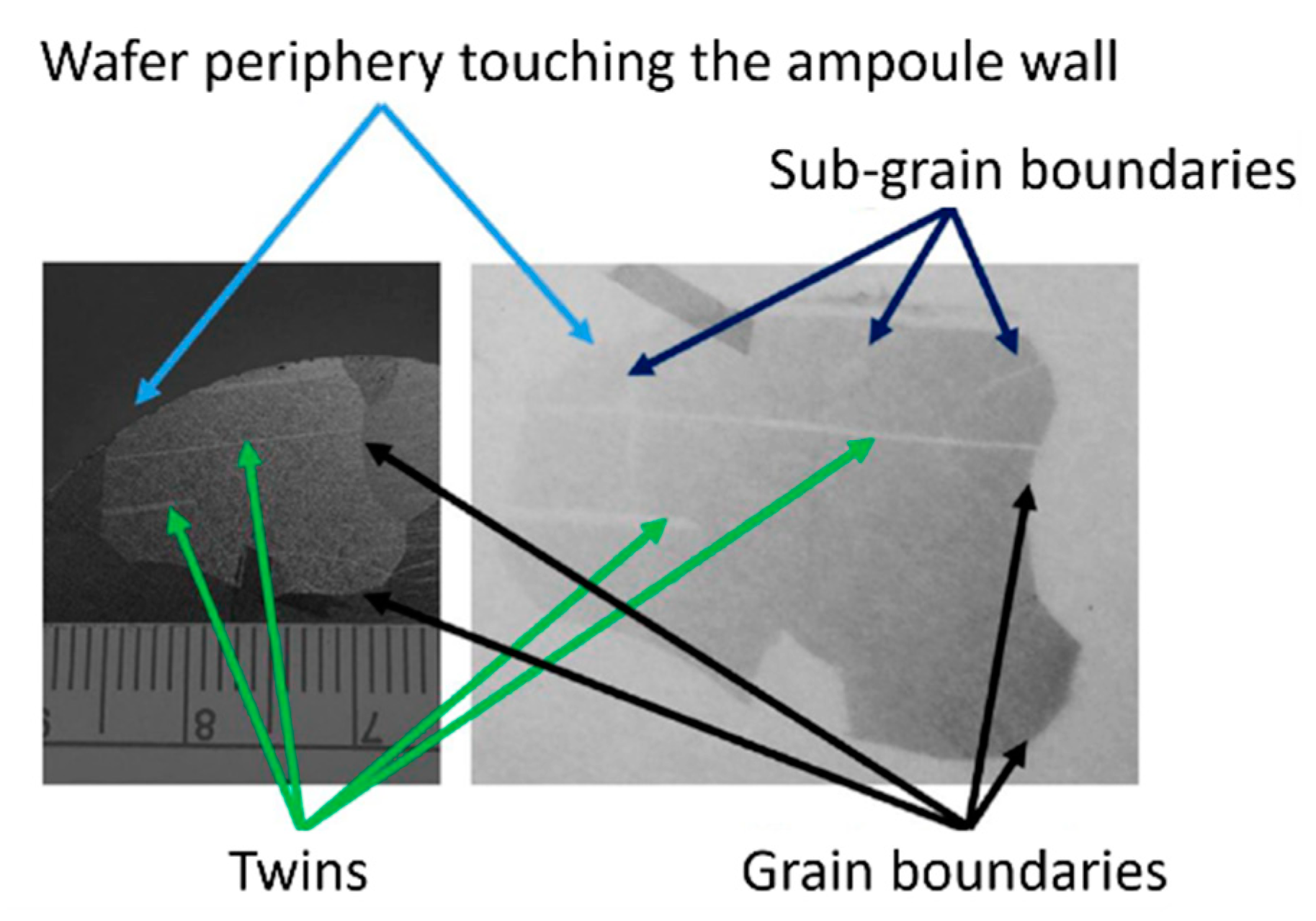
5.3. Crystal Characterization

The wafers cut from the ingot go through some screening measurements prior to the actual detector fabrication. The bare crystals are first studied using infrared (IR) transmission imaging to detect the presence of secondary phase Te inclusions or precipitates. It is common to find unreacted Te aggregating sporadically within the crystal volume during the crystallization process resulting in Te inclusions. While CZTS is transparent to IR photons, due to the narrow bandgap (0.3 eV) of tellurium, Te tends to absorb the IR photons. IR transmission imaging thus results in a contrast image clearly showing the Te inclusions as darker spots. The IR transmission microscopy system uses a large field-of-view microscope objective, a CCD camera, a motorized X-Y-Z translation stages, and an IR light source coupled with a wide-beam condenser for illuminating the samples. The sizes and concentrations of Te inclusions were evaluated by taking images at several locations evenly distributed along the long side of the crystal from two perpendicular directions. Figure 10 shows the IR transmission images of VBM and THM grown crystals [49]. A 5× magnification corresponding to a depth of focus of 14 mm was used. Each scan generated several stacked images and covered an area of 1.1 × 1.5 mm2. From the IR micrographs, the Te inclusion concentrations were calculated to be 4.3 × 10⁴ and 8 × 105 cm−3 for the THM and VBM crystals, respectively. It can be noticed that the concentration of the Te inclusions is an order of magnitude lower in the THM crystal compared to that of the VBM. The Te average inclusion sizes were measured to be about 8 µm. Te inclusions larger than 10 µm are known to be potential recombination centers in CZT detectors [51,52,53].
The crystals with a lower concentration of Te inclusions are then sorted for resistivity measurements. For these measurements, gold contacts are deposited on the two opposing faces meant to be the detector anode and cathode. The contacts generally cover the entire surface area barring the sides. An electric field is applied across the detector and the current flow across the thickness is measured using a sensitive current meter. The currents are on the order of sub-nA at electric fields on the order of 500 V/cm. Figure 11 shows the current-voltage characteristics typically observed in THM and VBM grown crystals. The bulk electrical resistivities were calculated to be on the order of 1010 Ω-cm. Such detectors are sorted for high resolution detector fabrication. Detectors that show resistivities below 109 Ω-cm are screened out. It can be noticed that the I V curves obtained in CZTS are not symmetric with respect to the bias polarity in general. This is mostly due to the different surface conditions at the two contact interfaces and is frequently observed in CZT detectors, as well [54,55]. Unlike CZT, reports on surface passivation to improve (lower) the surface conditions and leakage current is scarce. Egarievwe et al. reported an average improvement of 25% in the energy resolution measured for 59.6 keV gamma rays after passivating the CZTS surface with 10% aqueous solution of ammonium fluoride. However, they did not observe any noticeable improvement in the charge transport properties [25].
Apart from the above optical and electrical characterization, optoelectronic measurements such as Pockel’s effect [56,57] measurements are also carried out to study the modified electric field profile due to the Te secondary phase and other polarizing defects after the application of the external bias. Details of such studies to study the internal electric field in CZTS could be found in Refs. [23,58].

6. Charge Transport Properties of CZTS

The high resistivity crystals are further sorted based on their charge transport properties. High resolution detectors should exhibit high carrier mobility (µ) and carrier lifetimes (τ). A prevalent figure-of-merit is the mobility-lifetime (µτ) product of the carriers. The higher the µτ product is, the better is the chance of achieving high charge collection efficiency and energy resolution. The mobility or more specifically the drift mobility is defined as the drift velocity acquired by a charge carrier per unit electric field. The carrier lifetime is defined as the average time the charge carriers spend between its generation and recombination. The charge collection efficiency (CCE) is defined as the ratio of the amount charge produced at the detector output to the amount of charge generated by a particular radiation-detector interaction.

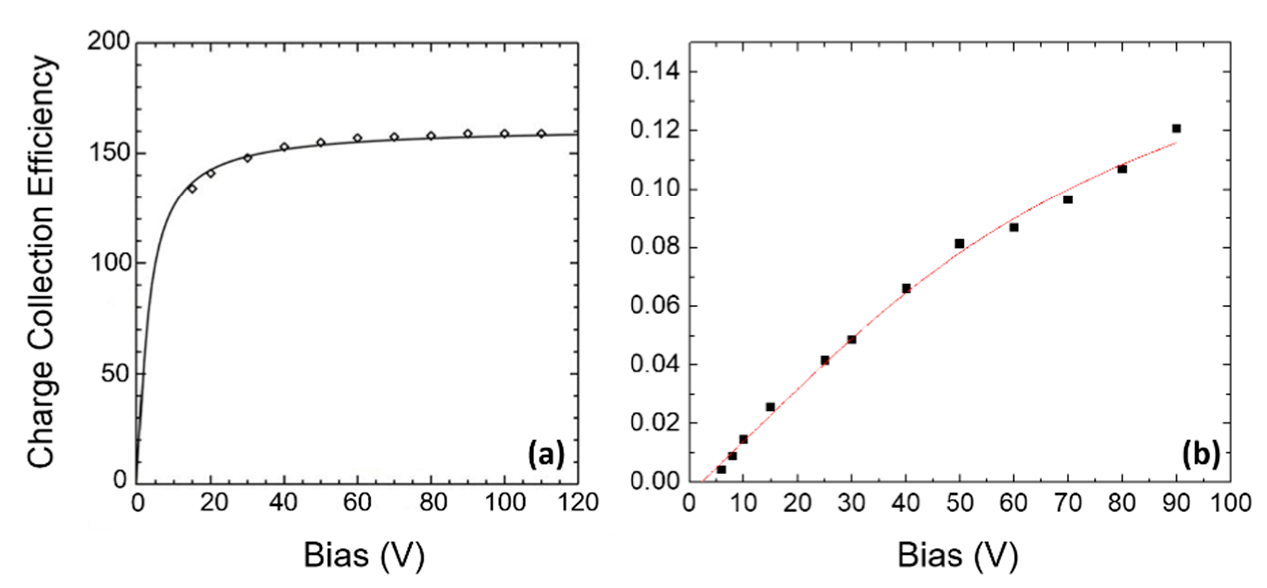
6.1. The µτ Product Measurement

The mobility-lifetime product measurement is based on the Hecht’s equation which relates the charge collection efficiency of a detector with the applied bias [59]. The detector in planar configuration is illuminated with energetic charged particles such as alpha particles. The alpha particles stop just below the detector surface where it creates a space charge comprised of electrons and holes. With a proper selection of the bias polarity either the electrons or the holes are made to transit the detector thickness. For instance, a positive bias at the detector entrance window will force electrons to traverse the detector thickness. The output detector signal (charge/current) in that case will be due to the electron transit. Similarly, a negative bias at the entrance window will result in a hole signal. The detector signal, which is proportional to the incident radiation energy, is picked up by a charge sensitive pre-amplifier to produce a voltage output proportional to the output (charge) of the detector. The pre-amplifier output is further filtered and amplified using a spectroscopic amplifier to improve the signal-to-noise ratio. A multichannel analyzer (MCA) determines the height (proportional to the incident energy) of each pulse and bins them into different channels to form a histogram of the distribution of events with different energies called the pulse height spectrum (PHS). The PHS shows peaks corresponding to the different incident energies. The width of the peak measured as full width at half maximum (FWHM) gives the resolution of the spectrometer. In general, in a PHS, the narrower the peak is, the higher the energy resolution. In addition, the further a peak is in terms of channel number in the MCA, the higher the corresponding energy. The MCA can be calibrated to express the channel numbers in energy (keV) units. A typical hybrid spectrometer that uses both analog and digital detection configuration used for the transport property measurements and radiation detection is shown in Figure 12.
To determine the µτ product, PHSs are acquired as a function of bias voltages starting from as low a bias as possible. For monoenergetic alpha particle sources only one peak will be present in each PHS, as the source emits alpha particles with a single average energy of E α . The energy corresponding to peak position ( E p ) is proportional to the output charge of the detector. The charge collection efficiency (η) is then calculated as the ratio E p / E α and plotted as a function of the bias V . The CCE vs. bias plot is fitted using a single-polarity Hecht equation given below as Equation (2) to determine the µτ product of a detector with thickness d .
η = μ τ V d 2 [ 1 e x p ( d 2 μ τ V ) ] .
Figure 13a shows a typical η V plot for electron transit obtained for a THM grown high-resolution CZTS ([Se] = 2 at%) detector [17]. The µτ product for electrons in this detector was calculated to be 6.6 × 10⁻³ cm2V−1. Chaudhuri et al. reported the hole µτ product for the first time measured using a 2-mm thick CZTS ([Se] = 3 at%) detector which produced an excellent hole signal when exposed to a 241Am radioisotope emitting 5486 keV alpha particles. The hole µτ product was calculated to be 8.5 × 10⁻⁵ cm2V−1. Figure 13b shows the corresponding η V plot. The electron µτ product obtained for the same crystal was calculated to be 6.4 × 10⁻⁴ cm2V−1 which is lower compared to that reported by Roy et al. [17]. In their most recent report, Roy et al. reported the electron µτ product to be in the range 4.0–6.5 × 10⁻³ cm2V−1. Pipek et al. measured the mobilities and lifetimes of both electrons and holes using a slightly different approach in THM grown CZTS ([Se] = 2 at%) detectors with a resistivity of 1.1 × 10¹⁰ Ω-cm [60]. They used the laser-induced transient-current technique with pulsed and dc bias in conjunction with Monte-Carlo simulation-based calculations for the transport properties studies. The electron and hole µτ product were calculated to be 1.9 × 10⁻³ and 1.4 × 10⁻⁴ cm2V−1, respectively.

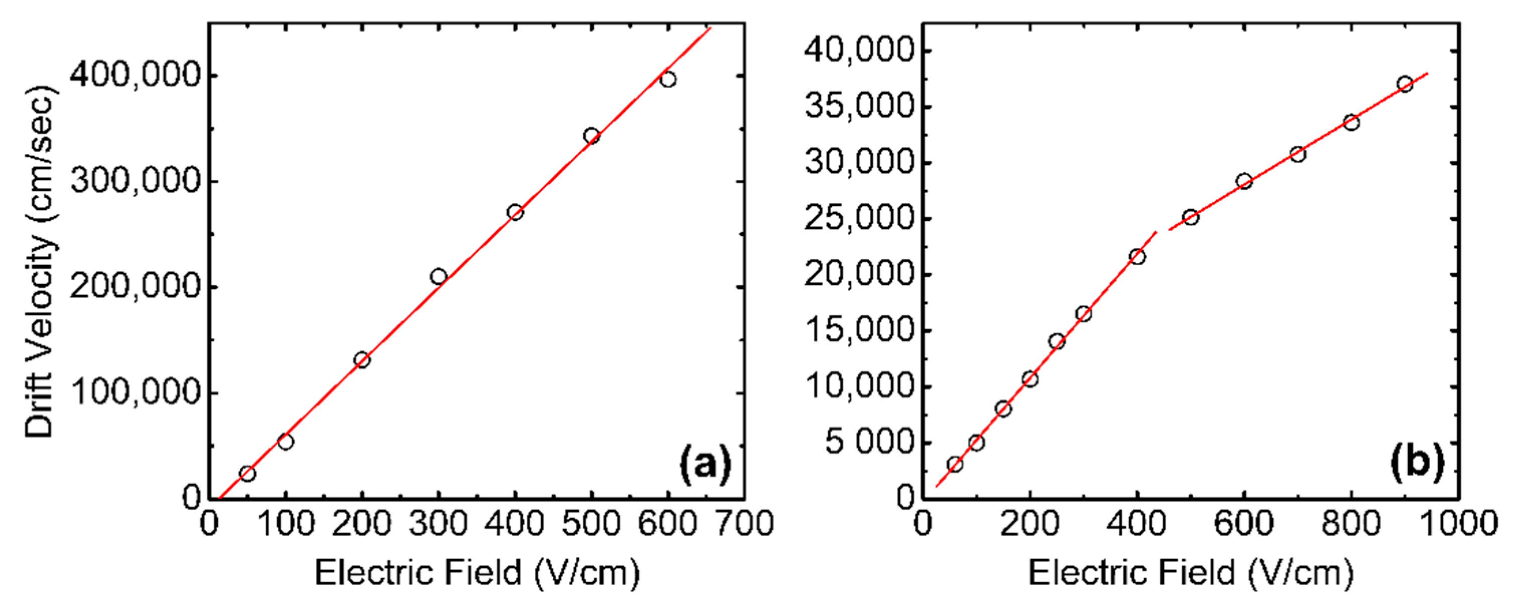
6.2. Drift Mobility Measurement

The drift mobility in semi-insulating thick crystals is usually measured using time-of-flight (TOF) techniques where an ionizing source is used to create charge pairs just beneath the detector (planar geometry) window surface. A bias V is applied to collect the charge pairs. The electrons or holes drift across the detector. This transit creates a signal at the output of the charge (current) sensitive pre-amplifier whose risetime (width) gives the transit duration ( t ) when plotted against time. Assuming a linear distribution of electric field across the detector, the drift velocity   v d of the charge carriers can be calculated as d / t , d being the detector thickness (therefore, it is necessary that the penetration depth of the ionizing radiation in the detector is negligible with respect to the detector thickness). To capture the charge (current) pulses, digital techniques are required to trace and store the pre-amplifier output digitally (Figure 12). Usually, a large number of such pulses are recorded for a particular bias and the average transit time is calculated. The experiment is repeated for several bias voltages and the drift-times are plotted against the corresponding electric field ( E ) calculated as ( V / d ). A plot of v d as a function of E is normally linear for moderate fields and a linear fit of the plot gives the drift mobility ( μ ) assuming the linear relationship v d = μ E . More details on the digital spectrometer used to determine the drift mobility using the TOF method can be found elsewhere [9]. Chaudhuri et al. reported the calculation of hole drift mobility in CZTS for the first time using a TOF method [21].
Figure 14 shows the variation of drift mobilities with an electric field that they obtained in a 2-mm thick VBM grown CZTS detector for both electrons and holes using a 241Am alpha source. The drift mobilities of the electron and holes were calculated to be 692 and 55 cm2V−1s−1, respectively. As mentioned above, Pipek et al. measured the electron and hole mobilities using a laser-induced transient-current technique with pulsed and dc bias in conjunction with Monte-Carlo simulation which turned out to be 830 and 40 cm2V−1s−1, respectively [60]. It can be noticed that the µτ product obtained by them were higher than that reported by Chaudhuri et al. Ref. [21] in their VBM grown detector by a factor of ~3. However, the carrier drift mobilities in the two detectors are comparatively closer. The lifetime of holes in both above studies were found to be longer than that of electrons. The electron and hole lifetimes as measured by Pipek et al. were 2.3 and 3.6 µs, respectively, whereas the same reported by Chaudhuri et al. were 1 and 1.5 µs.

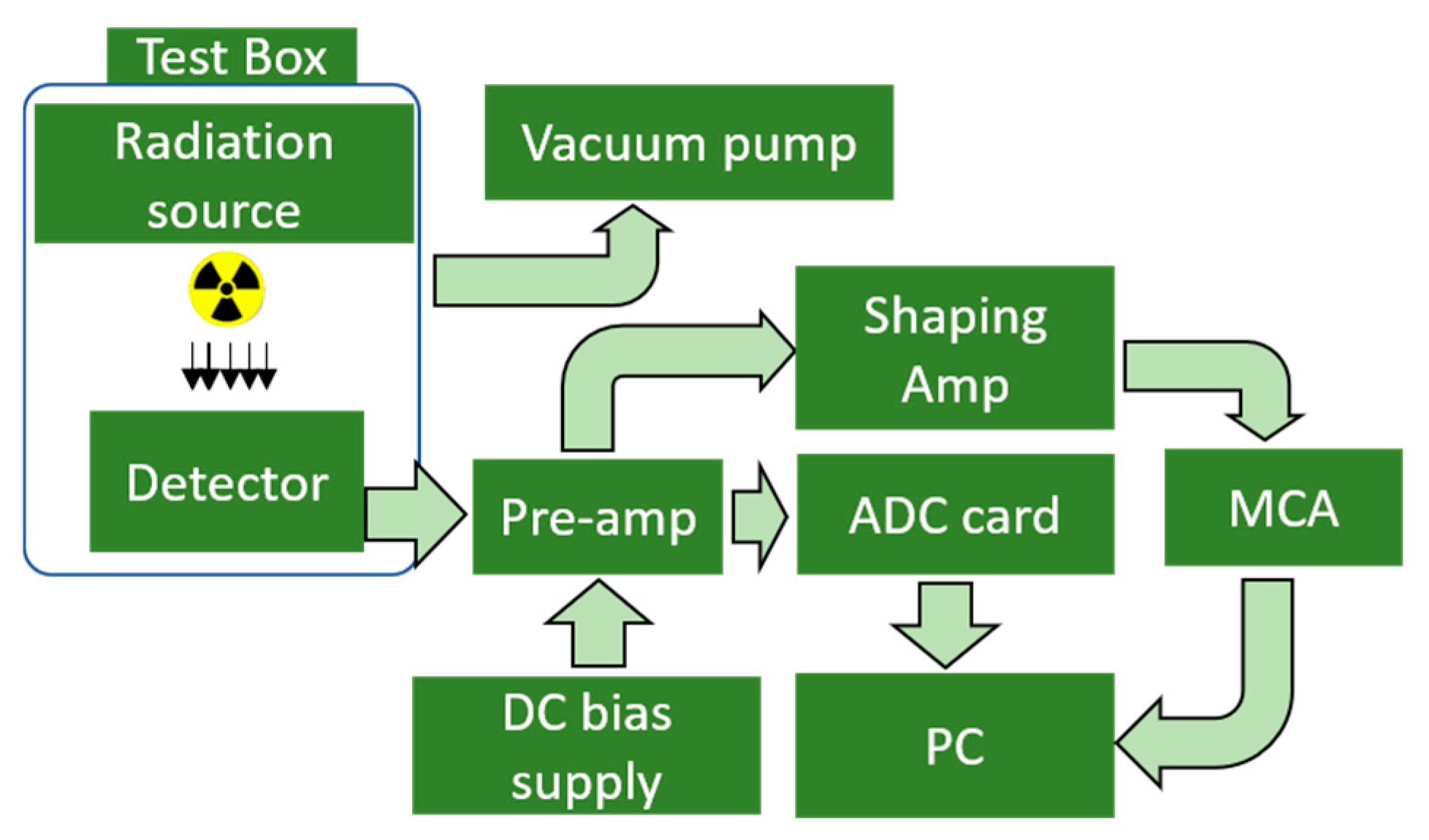
7. Radiation Detection with CZTS

The detectors that show the highest charge transport properties are selected for high-resolution detector fabrication. A detector responds quite differently to various radiations (different type, energy, etc.). Figure 15 shows the pulse shapes that are obtained using a VBM grown 2-mm thick CZT crystal for alpha and gamma ray exposure. It can be noticed that for the same alpha particle energy, the pulse shape (risetime and pulse height) varies drastically depending on whether the electrons or holes transit the detector thickness. On the other hand, the response to the gamma rays is even more different as gamma rays generally penetrate up to large distances and hence the movement of both the electrons and holes are reflected in the output signal. Regardless of the type of incident radiation, the pre-amplifier pulses are processed exactly as has been described in Section 6.2 to generate the PHS. CZTS detectors have demonstrated to exhibit gamma PHS with highly resolved peaks and other spectral features. Table 1 enlists the energy resolution reported by various groups using CZTS detectors exposed to gamma rays of different energies and Figure 16 shows the gamma-ray spectra obtained by Frisch collar CZTS detectors for various gamma-ray energies.
Although the application of digital correction methods had been reported abundantly for CZT and similar detectors [61,62,63,64], the only digital correction in CZTS gamma-ray spectra based on a biparametric correlation method has been reported by Chaudhuri et al. [21]. Figure 17a shows the gamma-ray PHS obtained using a planar CZTS detector exposed to a 137Cs source emitting 662 keV gamma rays.
It can be observed that the 662 keV gamma-ray photopeak was not well-resolved in the PHS. The corresponding biparametric correlation plot is shown in Figure 17b. The 662 keV events could be seen inclined towards the left implying charge loss which caused the observed broadening of the corresponding peak in the PHS. Figure 17c shows the biparametric plot with a digital correction scheme being applied to compensate for the charge-loss of the photoelectric events related to the 662 keV gamma rays. The PHS reconstructed from the corrected biparametric plot is shown in Figure 17d where all the spectral features including the peak width were seen to substantially improve.

8. Study of Intrinsic Defects in CZTS

Several groups have studied the electrically active intrinsic defects in CZTS single crystals that interfere with the high-resolution performance of the detectors. Yakimov et al. performed photo induced current transient spectroscopic studies in the horizontal Bridgman method grown CZTS and compared the results with a standard CZT detector grown and fabricated under similar conditions [23]. They observed four defect related peaks in the temperature scan range of 50–400 K using sub-bandgap (890 nm) laser excitation. Their results clearly demonstrated that the concentrations of the common defect centers with activation energies of 1.07 and 0.89 eV have dramatically (one order of magnitude) reduced in the CZTS detector. The PICTS results showed two peaks with activation energies of 0.73 and 0.19 eV which were not observed in the CZT detector. However, Yakimov et al. did not mention whether the observed energy levels were measured from the conduction band edge or the valence band edge. They also did not identify the observed defects. Gul et al. performed the current mode deep level transient spectroscopy (i-DLTS) in both VBM and THM grown CZTS and CZT detectors [65]. They reported the presence of both electron and hole traps in the temperature scan range of 10–400 K using a sub-bandgap excitation laser (850 nm). Three electron traps located at 0.022, 0.058, and 0.78 eV below the conduction band edge, and four hole traps located at 0.18, 0.26, 0.37, and 1.1 eV above the valence band edge were observed in the temperature scan range. Gul et al. had also identified the defect configuration in their report. Rejhon et al. used a rather non-conventional approach involving optical and temporal as well as temperature measurements of electrical field distribution to study the deep levels in CZTS that are responsible for influencing the internal electric field distribution in the detector [66]. They observed four defect centers out of which two were electron trap centers situated at 1.18 and 0.73 eV below the conduction band edge, one was a hole trap center situated at 0.83 eV above the valence band edge and one defect center situated at 0.83 eV below the conduction band edge (or 0.65 eV above the valence band edge) which could be either an electron or hole trap or a recombination level. In an earlier work, Rejhon et al. observed that the electrical transport properties of CZTS are governed by two deep levels close to the mid-bandgap—one recombination and one hole trap [67]. They also observed that the presence of hole traps indirectly enhances the µτ product of electrons. Pipek et al. measured the transients related to the electron- and hole-current triggered by pulsed and dc biases in a CZTS detector using a laser induced transient current technique in conjunction with numerical simulations [60]. They reported one shallow electron and one shallow hole trap center, and a strong recombination center located at 0.73 eV below the conduction band edge. Table 2 below summarizes the defect parameters that have been reported by various groups.
From Table 2, it can be observed that an electron trap center situated ~0.7 eV below the conduction band edge has been observed in all the published reports. The defect center has been identified as a doubly (positively) charged antisite T e C d + + center. The corresponding capture cross-section has been reported to be as high as 5 × 10⁻¹¹ cm2. The higher the capture cross-section for a trap center is, the higher the probability of a charge carrier of getting trapped in that trap. Hence, the T e C d + + center is a potential electron trap center in CZTS crystals. However, Rejhon et al. concluded that this level exhibits a weak optically induced electron transition to the conduction band [66]. A couple of deeper electron traps have also been reported located at 0.83 and 1.18 eV below the conduction band edge. The former is a potential recombination center and is reported to influence the internal electric field distribution in CZTS detector after application of the bias. It has also been reported to form a positive space charge at a steady state bias voltage [66]. Among the shallow electron traps impurity (Se) related defect centers have been reported. The corresponding low values of capture cross-sections indicate that these shallow levels are not potential traps.
Among the hole trap centers, levels situated at 0.18, 0.26, and 0.37 eV above the valence band edge have commonly been reported. The former two have been identified as Cd vacancy complexes (A centers) and singly (negatively) ionized tellurium interstitials ( T e i ), respectively, and the latter as a cadmium vacancy site V C d [65]. A deeper hole trap center situated at ~0.8 eV has been identified as a second ionized state of the cadmium vacancy by Rejhon et al. [66]. They also indicated that this defect level might be responsible for both thermally and optically induced decrease in a positive space charge after the application of the bias and infrared light. An even deeper hole trap level located at 1.1 eV above the valence band edge has been observed by Gul et al. [65] which has been identified as a possible Te-rich secondary phase T e S P .
The majority of the cases of the above defect identification are based on a comparison with the existing reported experimental and theoretical values for CZT. T e C d is the most dominant intrinsic trap center found in CZT grown in Te excess conditions besides cadmium vacancies V C d , which is a hole trap center [68]. The density functional theory based ab initio defect calculations for CZTS has been reported by Kleppinger et al. Their calculations established that there is an increase of at least 1 eV in the formation energy of TeCd and TeZn antisites in CZTS compared to that in CZT. The findings confirm that inclusion of selenium in the CZT matrix does help in reducing the formation of potential hole trap centers [49].

9. Role of Se Concentration in CZTS

Finally, in this section, we assess the role of the concentration of Se in CZTS in determining the detection performance. Roy et al. studied THM grown Cd0.9Zn0.1Te1−ySey with y = 0.015. 0.02, 0.04, and 0.07 [69]. They studied the resistivity, electron µτ product, X-ray topography, and IR transmission image for each composition. The X-ray topography studies found all the compositions to be free of sub-grain boundary networks. Resistivity and µτ products exhibited the highest values, 3 × 10¹⁰ Ω-cm and 6.6 × 10⁻³ cm2V−1, respectively for Se concentration of 2 at% (y = 0.02). The least concentration of Te-rich inclusions as observed from the IR transmission images, also corresponded to the atomic percentage of Se concentration of 2%.
Chaudhuri et al. investigated the role of Se concentration in their VBM grown Cd0.9Zn0.1Te1−ySey single crystals with y = 0.02. 0.03, 0.05, and 0.07 using current-voltage characteristics and radiation detection measurements [70]. While all the compositions showed a proper response to alpha particle radiation, only the composition with y = 0.03 (3 at%) produced gamma-ray spectrum. The rest three compositions showed a linear region with a slope lower than unity in the log Jlog V plots which indicates a current flow mechanism non-compliant with the space charge limited current.
While rigorous theoretical calculations are necessary to understand the appropriate role of the concentration of Se in controlling the crystal characteristics, the empirical consensus for the optimized Se concentration is in the range 2–3 at%.

10. Conclusions

In this article, we review the advances in Cd0.9Zn1.0Te1−ySey quaternary wide bandgap high-Z semiconductor for room-temperature high-energy gamma-ray detection since its inception as a high-resolution detector in the middle of the last decade. Since then, CZTS has been demonstrated to offer excellent charge transport properties and energy resolution. CZTS gained major attention since it has demonstrated unprecedented compositional homogeneity resulting in exceptionally high crystalline growth yield. Its ternary predecessor CZT, despite its high-resolution performance, had always demonstrated low crystal growth yield resulting in high production costs. The best energy resolution that has been reported for CZTS detector is ~0.77% for 662 keV gamma rays which is very close to the 0.5% (or less) target set by the US DOE.
X-ray topography, IR transmission imaging, and PICTS measurements have decisively proven that the addition of Se in a certain specific concentration, significantly reduces the secondary phase Te inclusion, sub-grain boundary networks, and other charge trapping intrinsic point defects when compared to CZT crystals. Ab initio defect calculations have shown that the formation of certain potential charge trapping centers is indeed inhibited when Se is placed in the substitutional position in the CZT matrix.
To date, three crystal growth approaches have been reported which are the travelling heater, vertical Bridgman, and horizontal Bridgman methods. The transport properties in CZTS have been observed to be better than most reported CZT detectors. Although the hole µτ product and mobility values in CZTS have been found to be an order of magnitude lower than those observed for electrons, the average hole lifetime has been found to be higher than that of electrons. The role of the concentration of Se in CZTS has also been studied by different groups and it has been seen that a 10 at% of Zn and a 2–3 at% of Se concentration gives the best crystal homogeneity and detection performance.
At present, the hole transport properties demonstrated by CZTS are much behind compared to that of the electrons. The high-resolution detection properties have been observed either in a single polarity charge sensing configuration or after application of digital correction methods. Extensive studies are required to investigate the cause of poor hole transport despite the reduction of hole traps such as secondary phase Te inclusion and sub grain boundary networks compared to CZT. Nevertheless, with exceptionally high crystal growth yield, high energy resolution performance, and impressive electron transport properties, CZTS is undoubtedly the next generation room-temperature gamma-ray detector, especially for spectroscopic and medical imaging applications.

Author Contributions

Conceptualization, funding acquisition, manuscript preparation, and editing, K.C.M.; conceptualization, manuscript preparation, literature survey, and characterization, S.K.C.; literature survey, DFT calculations, crystal growth, and characterization, J.W.K.; literature survey and crystal growth, R.N.; literature survey and crystal growth, O.K. All authors have read and agreed to the published version of the manuscript.

Funding

This research was funded by the DOE Office of Nuclear Energy’s Nuclear Energy University Program (NEUP), grant nos. DE-AC07-051D14517 and DE-NE0008662. The work was also supported in part by the Advanced Support Program for Innovative Research Excellence-I (ASPIRE-I), grant no. 15530-E404 and Support to Promote Advancement of Research and Creativity (SPARC), grant no. 15530-E422 of the University of South Carolina (UofSC), Columbia, USA.

Institutional Review Board Statement

Not applicable.

Informed Consent Statement

Not applicable.

Data Availability Statement

Data are contained within the article.

Acknowledgments

The authors acknowledge the support from the Powder X-ray Diffraction Facility at the Department of Chemistry and Biochemistry, UofSC; Electron Microscopy Center at UofSC for the SEM and EDX facility; and Stavros G. Karakalos of the Department of Chemical Engineering, UofSC for the XPS measurements.

Conflicts of Interest

The authors declare no conflict of interest.

References

  1. Schmidtlein, C.R.; Turner, J.N.; Thompson, M.O.; Mandal, K.C.; Häggström, I.; Zhang, J.; Humm, J.L.; Feiglin, D.H.; Krol, A. Initial performance studies of a wearable brain positron emission tomography camera based on autonomous thin-film digital Geiger avalanche photodiode arrays. J. Med. Imaging 2017, 4, 011003. [Google Scholar] [CrossRef] [PubMed] [Green Version]
  2. Johns, P.M.; Nino, J.C. Room temperature semiconductor detectors for nuclear security. J. Appl. Phys. 2019, 126, 040902. [Google Scholar] [CrossRef] [Green Version]
  3. Seco, J.; Clasie, B.; Partridge, M. Review on the characteristics of radiation detectors for dosimetry and imaging. Phys. Med. Biol. 2014, 59, R303–R347. [Google Scholar] [CrossRef] [PubMed] [Green Version]
  4. Rowland, J.; Kasap, S. Amorphous Semiconductors Usher in Digital X-Ray Imaging. Phys. Today 1997, 50, 24–30. [Google Scholar] [CrossRef]
  5. Owens, A.; Peacock, A. Compound semiconductor radiation detectors. Nucl. Instrum. Meth. Phys. Res. A 2004, 531, 18–37. [Google Scholar] [CrossRef]
  6. Schlesinger, T.E.; Toney, J.E.; Yoon, H.; Lee, E.Y.; Brunett, B.A.; Franks, L.; James, R.B. Cadmium zinc telluride and its use as a nuclear radiation detector material. Mater. Sci. Eng. R Rep. 2001, 2001 32, 103–189. [Google Scholar] [CrossRef]
  7. Szeles, C. CdZnTe and CdTe materials for X-ray and gamma ray radiation detector applications. Phys. Status Soldi B 2004, 241, 783–790. [Google Scholar] [CrossRef]
  8. Del Sordo, S.; Abbene, L.; Caroli, E.; Mancini, A.M.; Zappettini, A.; Ubertini, P. Progress in the development of CdTe and CdZnTe semiconductor radiation detectors for astrophysical and medical applications. Sensors 2009, 9, 3491–3526. [Google Scholar] [CrossRef] [PubMed]
  9. Sajjad, M.; Chaudhuri, S.K.; Kleppinger, J.W.; Mandal, K.C. Growth of large-area Cd0.9Zn0.1Te single crystals and fabrication of pixelated guard-ring detector for room-temperature γ-ray detection. IEEE Trans. Nucl. Sci. 2020, 67, 1946–1951. [Google Scholar] [CrossRef]
  10. Abbene, L.; Principato, F.; Gerardi, G.; Buttacavoli, A.; Cascio, D.; Battelli, M.; Amadè, N.S.; Seller, P.; Veale, M.C.; Fox, O.; et al. Room-temperature X-ray response of cadmium–zinc–telluride pixel detectors grown by the vertical Bridgman technique. J. Synchrotron Radiat. 2020, 27, 319–328. [Google Scholar] [CrossRef] [Green Version]
  11. Chen, H.; Awadalla, S.A.; Iniewski, K.; Lu, P.H.; Harris, F.; Mackenzie, J.; Hasanen, T.; Chen, W.; Redden, R.; Bindley, G. Characterization of large cadmium zinc telluride crystals grown by traveling heater method. J. Appl. Phys. 2008, 103, 014903. [Google Scholar] [CrossRef] [Green Version]
  12. Amman, M.; Lee, J.S.; Luke, P.N.; Chen, H.; Awadalla, S.A.; Redden, R.; Bindley, G. Evaluation of THM-grown CdZnTe material for large-volume gamma-ray detector applications. IEEE Trans. Nucl. Sci. 2009, 56, 795–799. [Google Scholar] [CrossRef]
  13. Roy, U.N.; Burger, A.; James, R.B. Growth of CdZnTe crystals by th travelling heater method. J. Cryst. Growth 2013, 379, 57–62. [Google Scholar] [CrossRef]
  14. James, R.B.; Schlesinger, T.E.; Lund, J.; Schieber, M. Cd1−xZnxTe spectrometers for gamma and x-ray applications. Semiconduct. Semimet. 1995, 43, 335–381. [Google Scholar] [CrossRef]
  15. Mandal, K.C.; Kang, S.H.; Choi, M.; Bello, J.; Zheng, L.; Zhang, H.; Groza, M.; Roy, U.N.; Burger, A.; Jellison, G.E.; et al. Simulation, modeling, and crystal growth of Cd0.9Zn0.1Te for nuclear spectrometers. J. Electron. Mater. 2006, 35, 1251–1256. [Google Scholar] [CrossRef]
  16. Zappettini, A.; Marchini, L.; Zha, M.; Benassi, G.; Zambelli, N.; Calestani, D.; Zanotti, L.; Gombia, E.; Mosca, R.; Zanichelli, M.; et al. Growth and characterization of CZT crystals by the vertical Bridgman method for x-ray detector applications. IEEE Trans. Nucl. Sci. 2011, 58, 2352–2356. [Google Scholar] [CrossRef] [Green Version]
  17. Roy, U.N.; Camarda, G.S.; Cui, Y.; Gul, R.; Yang, G.; Zazvorka, J.; Dedic, V.; Franc, J.; James, R.B. Evaluation of CdZnTeSe as a high-quality gamma-ray spectroscopic material with better compositional homogeneity and reduced defects. Sci. Rep. 2019, 9, 7303. [Google Scholar] [CrossRef] [PubMed] [Green Version]
  18. Mandal, K.C.; Kang, S.H.; Choi, M.; Kargar, A.; Harrison, M.J.; McGregor, D.S.; Bolotnikov, A.E.; Carini, G.A.; Camarda, G.S.; James, R.B. Characterization of low-defect Cd0.9Zn0.1Te and CdTe crystals for high-performance Frisch collar detector. IEEE Trans. Nucl. Sci. 2007, 35, 1251–1256. [Google Scholar] [CrossRef]
  19. Bolotnikov, A.E.; Ackley, K.; Camarda, G.S.; Cui, Y.; Eger, J.F.; De Geronimo, G.; Finfrock, C.; Fried, J.; Hossain, A.; Lee, W.; et al. High-efficiency CdZnTe gamma-ray detectors. IEEE Trans. Nucl. Sci. 2005, 62, 3193–3198. [Google Scholar] [CrossRef]
  20. Chaudhuri, S.K.; Sajjad, M.; Mandal, K.C. Pulse-shape analysis in Cd0.9Zn0.1Te0.98Se0.02 room-temperature radiation detectors. Appl. Phys. Lett. 2020, 116, 162107. [Google Scholar] [CrossRef] [Green Version]
  21. Chaudhuri, S.K.; Sajjad, M.; Kleppinger, J.W.; Mandal, K.C. Charge transport properties in CdZnTeSe semiconductor room-temperature γ-ray detectors. J. Appl. Phys. 2020, 127, 245706. [Google Scholar] [CrossRef]
  22. Hwang, S.; Yu, H.; Bolotnikov, A.E.; James, R.B.; Kim, K. Anomalous Te inclusion size and distribution in CdZnTeSe. IEEE Trans. Nucl. Sci. 2019, 66, 2329–2332. [Google Scholar] [CrossRef]
  23. Yakimov, A.; Smith, D.; Choi, J.; Araujo, S. Growth and characterization of detector-grade CdZnTeSe by horizontal Bridgman technique. Proc. SPIE 2019, 1114, 111141N. [Google Scholar] [CrossRef]
  24. Roy, U.N.; Camarda, G.S.; Cui, Y.; James, R.B. Advances in CdZnTeSe for radiation detector applications. Radiation 2021, 1, 123–130. [Google Scholar] [CrossRef]
  25. Egarievwe, S.U.; Roy, U.N.; Agbalagba, E.O.; Harrison, B.A.; Goree, C.A.; Savage, E.K.; James, R.B. Optimizing CdZnTeSe Frisch-grid nuclear detector for gamma-ray spectroscopy. IEEE Access 2020, 8, 137530–137539. [Google Scholar] [CrossRef]
  26. Yang, G.; Bolotnikov, A.E.; Fochuk, P.M.; Kopach, O.; Franc, J.; Belas, E.; Kim, K.H.; Camarda, G.S.; Hossain, A.; Cui, Y.; et al. Post-growth thermal annealing study of CdZnTe for developing room-temperature X-ray and gamma-ray detectors. J. Cryst. Growth 2013, 379, 16–20. [Google Scholar] [CrossRef]
  27. Chen, H.; Awadalla, S.A.; Mackenzie, J.; Redden, R.; Bindley, G.; Bolotnikov, A.E.; Camarda, G.S.; Carini, G.; James, R.B. Characterization of traveling heater method (THM) grown Cd0.9Zn0.1Te crystals. IEEE Trans. Nucl. Sci. 2007, 54, 811–816. [Google Scholar] [CrossRef]
  28. He, Z. Review of the Shockley–Ramo theorem and its application in semiconductor gamma-ray detectors. Nucl. Instrum. Meth. Phys. Res. A 2001, 463, 250–267. [Google Scholar] [CrossRef]
  29. Barrett, H.H.; Eskin, J.D.; Barber, H.B. Charge transport in arrays of semiconductor gamma-ray detectors. Phys. Rev. Lett. 1995, 75, 156–159. [Google Scholar] [CrossRef] [Green Version]
  30. Chaudhuri, S.K.; Krishna, R.M.; Zavalla, K.J.; Matei, L.; Buliga, V.; Groza, M.; Burger, A.; Mandal, K.C. Performance of Cd0.9Zn0.1Te based high-energy gamma detectors in various single polarity sensing device geometries. In Proceedings of the 2012 IEEE Nuclear Science Symposium and Medical Imaging Conference Record (NSS/MIC), Anaheim, CA, USA, 27 October–3 November 2012. [Google Scholar] [CrossRef]
  31. Krishna, R.M.; Muzykov, P.G.; Mandal, K.C. Electron beam induced current imaging of dislocations in Cd0.9Zn0.1Te crystal. J. Phys. Chem. Solids 2013, 74, 170–173. [Google Scholar] [CrossRef]
  32. Krishna, R.M.; Hayes, T.C.; Muzykov, P.G.; Mandal, K.C. Low temperature crystal growth and characterization of Cd0.9Zn0.1Te for radiation detection applications. Mater. Res. Soc. Symp. Proc. 2011, 1341, 203. [Google Scholar] [CrossRef]
  33. McGregor, D.S.; He, Z.; Seifert, H.A.; Wehe, D.K.; Rojeski, R.A. Single charge carrier type sensing with a parallel strip pseudo-Frisch-grid CdZnTe semiconductor radiation detector. J. Appl. Phys. 1998, 72, 792–794. [Google Scholar] [CrossRef] [Green Version]
  34. Luke, P.N. Single-polarity charge sensing in ionization detectors using coplanar electrodes. Appl. Phys. Lett. 1998, 65, 2884–2886. [Google Scholar] [CrossRef]
  35. Abbene, L.; Gerardi, G.; Pricipato, F.; Buttacavoli, A.; Altieri, S.; Protti, N.; Tomarchio, E.; Del Sordo, S.; Auricchio, N.; Bettelli, M.; et al. Recent advances in the development of high-resolution 3D cadmium–zinc–telluride drift strip detectors. J. Synchrotron Rad. 2020, 27, 1564–1576. [Google Scholar] [CrossRef] [PubMed]
  36. Fiederle, M.; Ebling, D.; Eiche, C.; Hofmann, D.M.; Salk, M.; Stadler, W.; Benz, K.W.; Meyer, B.K. Comparison of CdTe, Cd0.9Zn0.1Te and CdTe0.9Se0.1 crystals: Application for γ- and X-ray detectors. J. Cryst. Growth 1994, 138, 529–533. [Google Scholar] [CrossRef]
  37. Fiducia, T.A.M.; Mendis, B.G.; Li, K.; Grovenor, C.R.M.; Munshi, A.H.; Barth, K.; Sampath, W.S.; Wright, L.D.; Abbas, A.; Bowers, J.W.; et al. Understanding the role of selenium in defect passivation for highly efficient selenium-alloyed cadmium telluride solar cells. Nat. Energy 2019, 4, 504–511. [Google Scholar] [CrossRef] [Green Version]
  38. Chanda, S.; Ghosh, D.; Debnath, B.; Debbarma, M.; Bhattacharjee, R.; Chattopadhyay, S. Calculations of the structural and optoelectronic properties of cubic CdxZn1−xTe1−ySey semiconductor quaternary alloys using the DFT-based FP-LAPW approach. J. Comput. Electron. 2020, 19, 1–25. [Google Scholar] [CrossRef]
  39. Kim, K.; Hong, J.; Kim, S. Electrical properties of semi-insulating CdTe0:9Se0:1:Cl crystal and its surface preparation. J. Cryst. Growth 2008, 310, 91–95. [Google Scholar] [CrossRef]
  40. Roy, U.N.; Bolotnikov, A.E.; Camarda, G.S.; Cui, Y.; Hossain, A.; Lee, K.; Lee, W.; Tappero, R.; Yang, G.; Gul, R.; et al. High compositional homogeneity of CdTexSe1−x crystals grown by the Bridgman method. APL Mater. 2015, 3, 026102. [Google Scholar] [CrossRef]
  41. Gul, R.; Roy, U.N.; Egarievwe, S.U.; Bolotnikov, A.E.; Camarda, G.S.; Cui, Y.; Hossain, A.; Yang, G.; James, R.B. Point defects: Their influence on electron trapping, resistivity, and electron mobility-lifetime product in CdTexSe1−x detectors. J. Appl. Phys. 2015, 119, 025702. [Google Scholar] [CrossRef]
  42. Roy, U.N.; Camarda, G.S.; Cui, Y.; Gul, R.; Hossain, A.; Yang, G.; Zazvorka, J.; Dedic, V.; Franc, J.; James, R.B. Role of selenium addition to CdZnTe matrix for room-temperature radiation detector applications. Sci. Rep. 2019, 9, 1620. [Google Scholar] [CrossRef] [PubMed] [Green Version]
  43. Roy, U.N.; Camarda, G.S.; Cui, Y.; James, R.B. High-resolution virtual Frisch grid gamma ray detectors based on as-grown CdZnTeSe with reduced defects. Appl. Phys. Lett. 2019, 114, 232107. [Google Scholar] [CrossRef]
  44. Roy, U.N.; Camarda, G.; Cui, Y.; Yang, G.; James, R.B. Impact of selenium addition to the cadmium-zinc-telluride matrix for producing high energy resolution X-and gamma-ray detectors. Sci. Rep. 2021, 11, 10338. [Google Scholar] [CrossRef] [PubMed]
  45. Hays, E.; Moiseev, A.; Bolotnikov, A.E.; Thompson, D.J.; Kierans, C.A.; Bolotnikov, A.E.; Thompson, D.J.; Kierans, C. A position-sensitive high-resolution CdZnTe calorimeter for AMEGO. In American Astronomical Society Meeting Abstracts; American Astronomical Society: Washington, DC, USA, 2019; Volume 233, Available online: https://ui.adsabs.harvard.edu/#abs/2019AAS...23315826H/abstract (accessed on 15 July 2021).
  46. Chu, M.; Terterian, S.; Ting, S.; Wang, C.C.; Benson, J.D.; Dinan, J.H.; James, R.B.; Burger, A. Effects of excess tellurium on the properties of CdZnTe radiation detectors. J. Electron. Mater. 2003, 32, 778–782. [Google Scholar] [CrossRef]
  47. Yang, F.; Jie, W.; Zha, G.; Xi, S.; Wang, M.; Wang, T. The effect of indium doping on deep level defects and electrical properties of CdZnTe. J. Electron. Mater. 2020, 49, 1243–1248. [Google Scholar] [CrossRef]
  48. Soundararajan, R.; Lynn, K.G. Effects of excess tellurium and growth parameters on the band gap defect levels in CdxZn1−xTe. J. Appl. Phys. 2012, 112, 073111. [Google Scholar] [CrossRef]
  49. Kleppinger, J.W.; Chaudhuri, S.K.; Roy, U.N.; James, R.B.; Mandal, K.C. Growth of Cd0.9Zn0.1Te1−ySey single crystals for room temperature gamma-ray detection. IEEE Trans. Nucl. Sci. Early Access 2021. [Google Scholar] [CrossRef]
  50. Egarievwe, S.U.; Hossain, A.; Okwechime, I.O.; Gul, R.; James, R.B. Effects of chemomechanical polishing on CdZnTe x-ray and gamma-ray detectors. J. Electron. Mater. 2015, 44, 3194–3201. [Google Scholar] [CrossRef]
  51. Bolotnikov, A.E.; Abdul-Jaber, N.M.; Babalola, O.S.; Camarda, G.S.; Cui, Y.; Hossain, A.; Jackson, E.; Jackson, H.C.; James, J.A.; Kohman, K.T.; et al. Effects of Te inclusions on the performance of CdZnTe radiation detectors. IEEE Trans. Nucl. Sci. 2008, 55, 2757–2764. [Google Scholar] [CrossRef] [Green Version]
  52. Carini, G.A.; Bolotnikov, A.E.; Camarda, G.S.; Wright, W.G.; James, R.B.; Li, L. Effect of Te precipitates on the performance of CdZnTe detectors. Appl. Phys. Lett. 2006, 88, 143515–143517. [Google Scholar] [CrossRef] [Green Version]
  53. Sellin, P.J.; Davies, A.W.; Gkoumas, S.; Lohstroh, A.; Özsan, M.E.; Parkin, J.; Perumal, V.; Prekas, G.; Veale, M. Ion beam induced charge imaging of charge transport in CdTe and CdZnTe. Nucl. Instrum. Meth. Phys. Res. B 2008, 266, 1300–1306. [Google Scholar] [CrossRef]
  54. Crocco, J.; Bensalah, H.; Zheng, Q.; Corregidor, V.; Avles, E.; Castalsini, A.; Fraboni, B.; Cavalcoli, D.; Cavallini, A.; Vela, O.; et al. Study of asymmetries of Cd(Zn)Te devices investigated using photo-induced current transient spectroscopy, Rutherford backscattering, surface photo-voltage spectroscopy, and gamma ray spectroscopies. J. Appl. Phys. 2012, 112, 074503. [Google Scholar] [CrossRef]
  55. Brovko, A.; Amzallag, O.; Adelberg, A.; Chernyak, L.; Raja, P.V.; Ruzin, A. Effects of oxygen plasma treatment on Cd1−xZnxTe material and devices. Nucl. Instrum. Meth. Phys. Res. B 2021, 1004, 165343. [Google Scholar] [CrossRef]
  56. Zumbiehl, A.; Hage-Ali, M.; Fougeres, P.; Koebel, J.M.; Regal, R.; Siffert, P. Electric field distribution in CdTe and Cd1−xZnxTe nuclear detectors. J. Cryst. Growth 1999, 197, 650–654. [Google Scholar] [CrossRef]
  57. Yang, G.; Bolotnikov, A.E.; Camarda, G.S.; Cui, Y.; Hossain, A.; Yao, H.W.; James, R.B. Internal electric field investigations of a cadmium zinc telluride detector using synchrotron X-ray mapping and Pockels effect measurements. J. Electron. Mater. 2009, 38, 1563–1567. [Google Scholar] [CrossRef]
  58. Dědič, V.; Fridrišek, T.; Franc, J.; Kunc, J.; Rejhon, M.; Roy, U.N.; James, R.B. Mapping of inhomogeneous quasi-3D electrostatic field in electro-optic materials. Sci. Rep. 2021, 11, 2154–3010. [Google Scholar] [CrossRef]
  59. Hecht, K. Zum mechanismus des lichtelektrischen primärstromes in isolierenden kristallen. Z. Phys. 1932, 77, 235–245. [Google Scholar] [CrossRef]
  60. Pipek, J.; Betušiak, M.; Belas, E.; Grill, R.; Praus, P.; Musiienko, A.; Pekarek, J.; Roy, U.N.; James, R.B. Charge transport and space-charge formation in Cd1−xZnxTe1−ySey radiation detectors. Phys. Rev. Appl. 2021, 15, 054058. [Google Scholar] [CrossRef]
  61. Chaudhuri, S.K.; Lohstroh, A.; Nakhostin, M.; Sellin, P.J. Digital pulse height correction in HgI2 γ-ray detectors. J. Instrum. 2012, 7, T04002. [Google Scholar] [CrossRef]
  62. Verger, L.; Boitel, M.; Gentet, M.C.; Hamelin, R.; Mestais, C.; Mongellaz, F.; Rustique, J.; Sanchez, G. Characterization of CdTe and CdZnTe detectors for gamma-ray imaging applications. Nucl. Instrum. Methods Phys. Res. A 2001, 458, 297–309. [Google Scholar] [CrossRef]
  63. Chaudhuri, S.K.; Zavalla, K.J.; Krishna, R.M.; Mandal, K.C. Biparametric analyses of charge trapping in Cd0.9Zn1.0Te based virtual Frisch grid detectors. J. Appl. Phys. 2013, 113, 074504. [Google Scholar] [CrossRef] [Green Version]
  64. Bolotnikov, A.E.; Butcher, J.; Camarda, G.S.; Cui, Y.; De Geronimo, G.; Fried, J.; Gul, R.; Fochuk, P.M.; Hamade, M.; Hossain, A.; et al. Array of virtual Frisch-grid CZT detectors with common cathode readout for correcting charge signals and rejection of incomplete charge-collection events. IEEE Trans. Nucl. Sci. 2012, 59, 1544–1551. [Google Scholar] [CrossRef]
  65. Gul, R.; Roy, U.N.; Camarda, G.S.; Hossain, A.; Yang, G.; Vanier, P.; Lordi, V.; James, R.B. A comparison of point defects in Cd1−xZnxTe1−ySey crystals grown by Bridgman and traveling heater methods. J. Appl. Phys. 2017, 121, 125705. [Google Scholar] [CrossRef]
  66. Rejhon, M.; Dědič, V.; Beran, L.; Roy, U.N.; Franc, J.; James, R.B. Investigation of deep levels in CdZnTeSe crystal and their effect on the internal electric field of CdZnTeSe gamma-ray detector. IEEE Trans. Nucl. Sci. 2019, 66, 1952–1958. [Google Scholar] [CrossRef]
  67. Rejhon, M.; Franc, J.; Dedic, V.; Pekárek, J.; Roy, U.N.; Grill, R.; James, R.B. Influence of deep levels on the electrical transport properties of CdZnTeSe detectors. J. Appl. Phys. 2018, 124, 235702. [Google Scholar] [CrossRef] [Green Version]
  68. Carvalho, A.; Tagantsev, A.; Öberg, S.; Briddon, P.R.; Setter, N. Intrinsic defects in CdTe and CdZnTe alloys. Phys. B. 2009, 404, 5019–5021. [Google Scholar] [CrossRef]
  69. Roy, U.N.; Camarda, G.S.; Cui, Y.; James, R.B. Optimization of selenium in CdZnTeSe quaternary compound for radiation detector applications. Appl. Phys. Lett. 2021, 118, 152101. [Google Scholar] [CrossRef]
  70. Chaudhuri, S.K.; Sajjad, M.; Kleppinger, J.W.; Mandal, K.C. Correlation of space charge limited current and γ-ray response of CdxZn1−xTe1−ySey room-temperature radiation detectors. IEEE Electron Device Lett. 2020, 41, 1336–1339. [Google Scholar] [CrossRef]
Figure 1. Optical photograph of grain boundaries observed in a typical THM grown CZTS crystal (left) and the corresponding X-ray topographic image (Adapted from Roy et al. Sci. Rep. 20199, 1620. Copyright 2019 Nature Research under Creative Commons Attribution 4.0 International License.]).
Crystals 11 00827 g001
Figure 2. Representation of 64 atom primitive supercell used for the DFT calculations for single crystals of (a) defect free CZT; (b) CZTS showing one Te atom replaced by a Se atom in the CZT zinc-blend matrix.
Crystals 11 00827 g002
Figure 3. (a) The schematics of a Frisch grid detector. (b) The variation of weighting potential as a function of time with and without the grid for a planar detector geometry, v is the drift velocity. (c) The variation of weighting potential as a function of position for a planar detector geometry. (d) The evolution of the detector signal in the cases of charge transit without trapping, repeat trapping and detrapping, and trapping followed by recombination leading to partial charge collection.
Crystals 11 00827 g003
Figure 4. Variation of concentration (at%) of Se and Zn, (a) and bandgap (b) along the ingot axis of a THM grown Cd0.9Zn0.1Te0.97Se0.02 crystal (Adapted from ref. [42] Copyright 2019 Nature Research under Creative Commons Attribution 4.0 International License).
Crystals 11 00827 g004
Figure 5. Schematics of a vertical furnace arrangement for vertical Bridgman growth.
Crystals 11 00827 g005
Figure 6. Powder X-ray diffractogram (a) survey scan using XPS (b) and EDX scan. (Adapted with permission from ref. [49]. Copyright 2021, IEEE) (c) of Cd0.9Zn0.1Te0.97Se0.03 grown using a VBM growth at UofSC.
Crystals 11 00827 g006
Figure 7. Cross-sectional view of a Cd0.9Zn0.1Te0.97Se0.02 ingot grown using a VBM method at UofSC. The grain boundaries have been emphasized with white lines for ease of visualization.
Crystals 11 00827 g007
Figure 8. (a) A 2-inch diameter Cd0.9Zn0.1Te0.97Se0.02 ingot grown using a VBM at UofSC. (b) A mechanically polished square wafer cut out from a VBM-grown ingot. (c) A 2-inch diameter CZTS boule grown using THM at BNL. (d) A 2-inch diameter THM-grown CZTS polished wafer (Adapted with permission from ref. [49] Copyright 2021, IEEE).
Crystals 11 00827 g008
Figure 9. CZTS detectors in various detector configurations: (a) A planar 10 × 10 × 2 mm3 with square contacts. (b) A 10 × 10 × 2 mm3 single pixel with circular contacts. (c) A 4.4 × 4.4 × 10.7 mm3 Frisch collar detector. The Frisch collar detector was fabricated at SRNL (Adapted with permission from ref. [49]. Copyright 2021, IEEE).
Crystals 11 00827 g009
Figure 10. IR micrographs obtained from (a) THM grown Cd0.9Zn0.1Te0.97Se0.02 crystal and (b) a VBM grown Cd0.9Zn0.1Te0.97Se0.03 crystal. The scan covered an area of ~1.1 × 1.5 mm2. The images have been cropped for better visibility (Adapted with permission from ref. [49]. Copyright 2021, IEEE).
Crystals 11 00827 g010
Figure 11. Current voltage (I-V) characteristics as obtained using a VBM grown (a) and THM grown (b) Cd0.9Zn0.1Te0.97Se0.02 planar detector. The I-V characteristics of the THM detector have been reproduced with permission from ref. [49]. Copyright 2021, IEEE. The inset in (a) shows the low-range I-V plot for resistivity calculations.
Crystals 11 00827 g011
Figure 12. Schematics of a hybrid radiation spectrometer which can acquire analog PHS, as well as digital pulse shapes from a detector. The vacuum pump is used to evacuate the test box for alpha particle measurements.
Crystals 11 00827 g012
Figure 13. Charge collection efficiency measured as a function of bias voltage for (a) electrons in a THM grown Cd0.9Zn0.1Te0.97Se0.02 (Adapted from ref. [17]. Copyright 2019 Nature Research under Creative Commons Attribution 4.0 International License) and (b) holes in a VBM grown Cd0.9Zn0.1Te0.97Se0.03 planar detector (Adapted with permission from ref. [21]. Copyright 2020, AIP Publishing). The solid lines are the Hecht equation fit. Note that the charge collection efficiency in (a) is expressed as the MCA channel number.
Crystals 11 00827 g013
Figure 14. Variation of drift mobilities as a function of electric field measured for electrons (a) and holes (b) in a VBM grown Cd0.9Zn0.1Te0.97Se0.03 planar detector (Adapted with permission from ref. [21]. Copyright 2021, AIP Publishing). The solid lines are the straight line fit to obtain the mobilities. Note the two separate slopes in the mobility plot for holes.
Crystals 11 00827 g014
Figure 15. (a) Pulse shapes obtained for electrons and hole transits across a VBM grown Cd0.9Zn0.1Te0.97Se0.03 planar detector using the 241Am alpha particle source. (b) Pulse shape for composite electron-hole transit when the detector was exposed to the 137Cs gamma-ray (662 keV) source (Adapted with permission from ref. [21]. Copyright 2021, IEEE).
Crystals 11 00827 g015
Figure 16. Gamma-ray PHS obtained from a THM grown Cd0.9Zn0.1Te0.97Se0.02 Frisch collar detector with dimensions ~ 4.5 × 4.5 × 10.8 mm3 with a 3-mm long Frisch grid for various gamma-ray energies. The detector was biased at 3000 V for the above measurements (Adapted from ref. [17]. Copyright 2019 Nature Research under Creative Commons Attribution 4.0 International License).
Crystals 11 00827 g016
Figure 17. (a) 137Cs gamma-ray PHS obtained from an as-fabricated VBM grown Cd0.9Zn0.1Te0.97Se0.03 planar detector. (b) The corresponding biparametric correlation plot. (c) The corrected biparametric plot using a digital correction scheme. (d) The corrected PHS regenerated from the corrected biparametric plot (Adapted with permission from ref. [21]. Copyright 2020, AIP Publishing).
Crystals 11 00827 g017
Table 1. Reported values of energy resolution obtained using THM and VBM grown CZTS detectors in different geometries.
RadioisotopeCrystal/Detector TypeGamma-Ray Energy (keV)Energy Resolution
(%)
133BaTHM/Frisch collar316.4 a, 9.0 b, 15.0 c
814.8 a, 4.6 b
2761.77 a, 2.0 b, 1.43 c
3031.7 a, 1.7 b, 1.36 c
3561.7 a, 1.6 b, 1.28 c
3841.2 a, 1.49 c
22NaTHM/Frisch collar5111.34 a, 1.26 c
137Cs6620.9 a, 1.07 b, 0.77 c
137CsVBM/Planar2.0 d,*
22NaTHM/Frisch collar12751.0 b, 0.56 c
a Roy et al. [43]. b Roy et al. [17]. c Roy et al. [44]. d Chaudhuri et al. [21]. * A digital correction method has been used.
Table 2. Intrinsic defects observed in CZTS single crystals, and the related parameters reported by various groups. E C and E V represents the conduction and valence band edge, respectively. The concentration of Zn in all the CZTS samples is 10%.
Defect Energy
Level
(eV)
Possible
Defect Identity
Capture Cross
Section
(cm2)
Crystal Type
0.19-1 × 10⁻¹⁹Horizontal Bridgman a
0.73-1 × 10⁻¹²
0.82-5 × 10⁻¹¹
1.02-7 × 10⁻¹¹
E C 0.022 Donor impurity9 × 10−21Bridgman ([Se] = 2%); THM ([Se] = 7%) b
E C 0.058 Se related donor5 × 10−17
E v + 0.18 A-center1 × 10−16
E v + 0.26 T e i 1 × 10⁻¹⁴
E v + 0.37 V C d 1 × 10⁻¹⁵Bridgman ([Se] = 2%) b
E C 0.78 T e C d + + 5 × 10⁻¹¹THM ([Se] = 7%) b
E v + 1.1 T e S P 1 × 10⁻¹⁰Bridgman ([Se] = 2%) b
E C 0.73 --[Se] = 4% c
E v + 0.83 -1 × 10⁻¹³
E C 1.18 --
E C 0.83 / E v + 0.65 -1 × 10⁻¹¹/1 × 10−15
E C 0.73 / E v + 0.79 Recombination center3.5 × 10−14/6.5 × 10−14THM ([Se] = 4%) d
a Yakimov et al. [23]. b Gul et al. [65]. c Rejhon et al. [66]. d Pipek et al. [60].
Publisher’s Note: MDPI stays neutral with regard to jurisdictional claims in published maps and institutional affiliations.

