Article

Change in Interface Characteristics of ITO Modified with n-decyltrimethoxysilane

1
Division of Electronic Engineering, Silla University, 140 Baegyang-daero (Blvd.) 700beon-gil (Rd), Sasang-gu, Busan 46958, Korea
2
Division of Materials Science and Engineering, Silla University, 140 Baegyang-daero (Blvd.) 700beon-gil (Rd), Sasang-gu, Busan 46958, Korea
3
SFC CO., LTD., 653-9 Gang-ni, Ochang-eup, Cheongwon-gun, Chugbuk 363-881, Korea
4
School of Electrical, Electronic and Control Engineering, Changwon National University, 20 Changwondaehak-ro, Uichang-gu, Changwon-si, Gyeongsangnam-do 51140, Korea
5
Department of Mechatronics Convergence, Changwon National University, 20 Changwondaehak-ro, Uichang-gu, Changwon-si, Gyeongsangnam-do 51140, Korea
*
Authors to whom correspondence should be addressed.
Crystals 2020, 10(8), 645; https://doi.org/10.3390/cryst10080645
Submission received: 9 June 2020 / Revised: 8 July 2020 / Accepted: 24 July 2020 / Published: 27 July 2020

Abstract

:
Herein, we examined changes in the interfacial properties of organic light-emitting diodes when n-decyltrimethoxysilane (CH3SAM) was deposited on the surface of an indium tin oxide (ITO) electrode for various deposition times. It was revealed that the interfacial properties varied with deposition time. As the latter increased, so did the measured value of the contact angle, and ITO substrate exhibited a lower wettability. The contact angle measurements for bare ITO at 1, 10, 30, and 90 min were 57.41°, 63.43°, 73.76°, 81.47°, respectively, and the highest value obtained was 93.34°. In addition, the average roughness and work function of the ITO were measured using atomic force microscopy and X-ray photoelectron spectroscopy. As the deposition time of CH3SAM on the ITO substrates increased, it was evident that the former was well aligned with the latter, improving surface modification. The work function of CH3SAM, modified on the ITO substrates, improved by approximately 0.11 eV from 5.05–5.16 eV. The introduction of CH3SAM to the ITO revealed the ease of adjustment of the characteristics of ITO substrates.

1. Introduction

Organic light-emitting diodes (OLEDs) are light-emitting devices comprising multiple stacked layers of organic materials. In OLEDs, when electrons and holes generated by electric fields are applied to organic materials inserted between the anode and the cathode, light is emitted through electrostatic miraculous attraction [1]. OLEDs have many advantages, including low power consumption, self-luminescence, wide viewing angle and full color, high reproducibility, ultra-thin, lightweight, fast response and the ability to drive with simple manufacturing processes. Due to these advantages, OLEDs have recently attracted attention as a promising high-tech development in the industrial sector [2,3].
Transparent conductive oxides (TCOs) with high transparency and low sheet resistance in visible light range (380–760 nm) have been widely used as transparent electrodes in optoelectronic devices [4,5]. Among them, indium tin oxide (ITO) is the most commonly used anode material in OLEDs due to its excellent hardness, chemical stability, high transparency and low resistivity [6].
However, ITO has a lower work function than that of other organic materials commonly used in OLEDs [7]. The large work function difference between ITO and organic materials, namely, the huge injection barrier, results in high driving voltage and low efficiency of OLED devices.
Many researchers have studied various methods to improve the injection barrier between the anode and the hole transport material (HTM). ITO modification can improve hole injection efficiency by reducing the injection barrier between the anode and the HTM. hole injection Compound used in ITO and HTM are Poly(3,4-ethylenedioxythiophene):poly(styrenesulfonate) (PEDOT:PSS) [8], Dipyrazino[2,3-f:2′,3′-h]quinoxaline-2,3,6,7,10, 11-hexacarbonitrile (HAT-CN) [9], Di-[4-(N,N-di-p-tolyl-amino)-phenyl] cyclohexane (TAPC) [10], and oxygen plasma treatment [11]. These approaches have brought improvements to hole injection, turn-on voltage, luminance, and stability [12]. Among the various formats for these layers, the most widely used surface-treatable format is a self-assembled monolayer (SAM), which is a well-ordered organic molecular membrane that can spontaneously organize on the surface of a substrate [13,14]. The structure of SAMs is largely divided into three parts: head group, alkyl chain, and functional group. The headgroup is chemically adsorbed on the surface of the substrate to form a closed-packed monolayer. Alkyl chains form well-aligned monolayers by van der Waals forces between different molecules, and the functional group can be varied as needed, which enables SAM to be applied to various fields. SAMs have been applied to micro lenses [15], corrosion inhibitors [16], solar cells [17], biological processes [18], and biosensors [19].
The carrier can be balanced by controlling the work function of the ITO through SAM modification and reducing the hole injection barrier with the HTM. The modification of the SAM on the ITO surface can balance the carrier by controlling the ITO work function and reducing the hole injection barrier between ITO and the HTM [20,21], and reduce the surface energy by reducing the amount of hydroxyl (-OH) groups present on the ITO surface [22]. In addition, the structural characteristics of the SAM is well aligned to expose the surface terminal functional group, the surface characteristics can be controlled by molecular units using the functional group. If the functional groups such as -CH3, -CF3 are present at the end of the SAM, the surface has hydrophobic properties and if it has functional groups such as -OH, -COOH, it has hydrophilic properties.
Herein, we used n-decyltrimethoxysilane (CH3SAM) with a methyl (-CH3) group as a terminal functional group to reduce the -OH groups present on the ITO surface, as well as to eliminate the large injection barrier between the anode and the HTM. We will review the surface properties according to the deposition time of CH3SAM on the ITO substrate.

2. Experimental Method

2.1. Materials

The ITO used for the positive electrode was a product of AMG Co., Ltd. (Prides Crossing, MA, USA), and it was deposited to a thickness of 150 ± 10 nm. The layer exhibited a sheet resistance of ≤10 Ω/sq and a transmittance of ≥85%, λ = 550 nm. CH3SAM was purchased from Gelest (Bucks County, PA, USA) for the SAM.

2.2. ITO Cleaning and Preparation

The surface of the ITO substrate was ultrasonically cleaned for 5 min with deionized (DI) water, acetone, DI water, and isopropanol alcohol (IPA), in that order. After exposure to N2 gas to remove moisture, the ITO was kept on a hot plate for 5 min at 150 °C to allow sufficient drying.

2.3. SAM Modification of the ITO Surface

SAMs are regularly well-aligned organic molecular membranes that spontaneously coat the surface of a given substrate [21]. The molecular structure consists of a head group that chemically adsorbs to the substrate, a central alkyl chain that allows for regular molecular film formation, and a functional group that influences the activity of the molecular film. In this experiment, we used CH3SAM, which has a -CH3 head group, while the alkyl chain in the central portion consists of hydrogen and carbon. The bonding component consists of triethoxysilane. The molecular structure of CH3SAM is shown in Figure 1.
Deposition of CH3SAM on the surface of the ITO substrate was achieved as follows: After putting the washed ITO and 7 mL PFA jar into a 500 mL PFA jar, CH3SAM was dropped into the 7 mL PFA jar. Thin film deposition was carried out by vapor phase methods at 120 °C in an electric oven.
The deposited ITO substrate was washed with IPA for 5 min to remove any physically adsorbed SAM. To examine the extent of SAM surface coverage on the ITO substrates with deposition time, we set the deposition times as 1 min, 10 min, 30 min, and 90 min, and included bare ITO for comparison. To evaluate the differences in the surface characteristics of the SAM over time, we measured the contact angle, average roughness, and work function. The contact angle was measured by a contact angle analyzer from Surface tech (GSX), while the average roughness was determined, in a non-contact mode, by a scanning probe microscope from Park Systems (NX20). NCHR of Park Systems Co., Ltd. (Suwon, Korea) was used as tip, and the work function was measured a by Hitachi High Tech (AC-2) photoelectron spectrometer (Hitachi Inc., Tokyo, Japan).

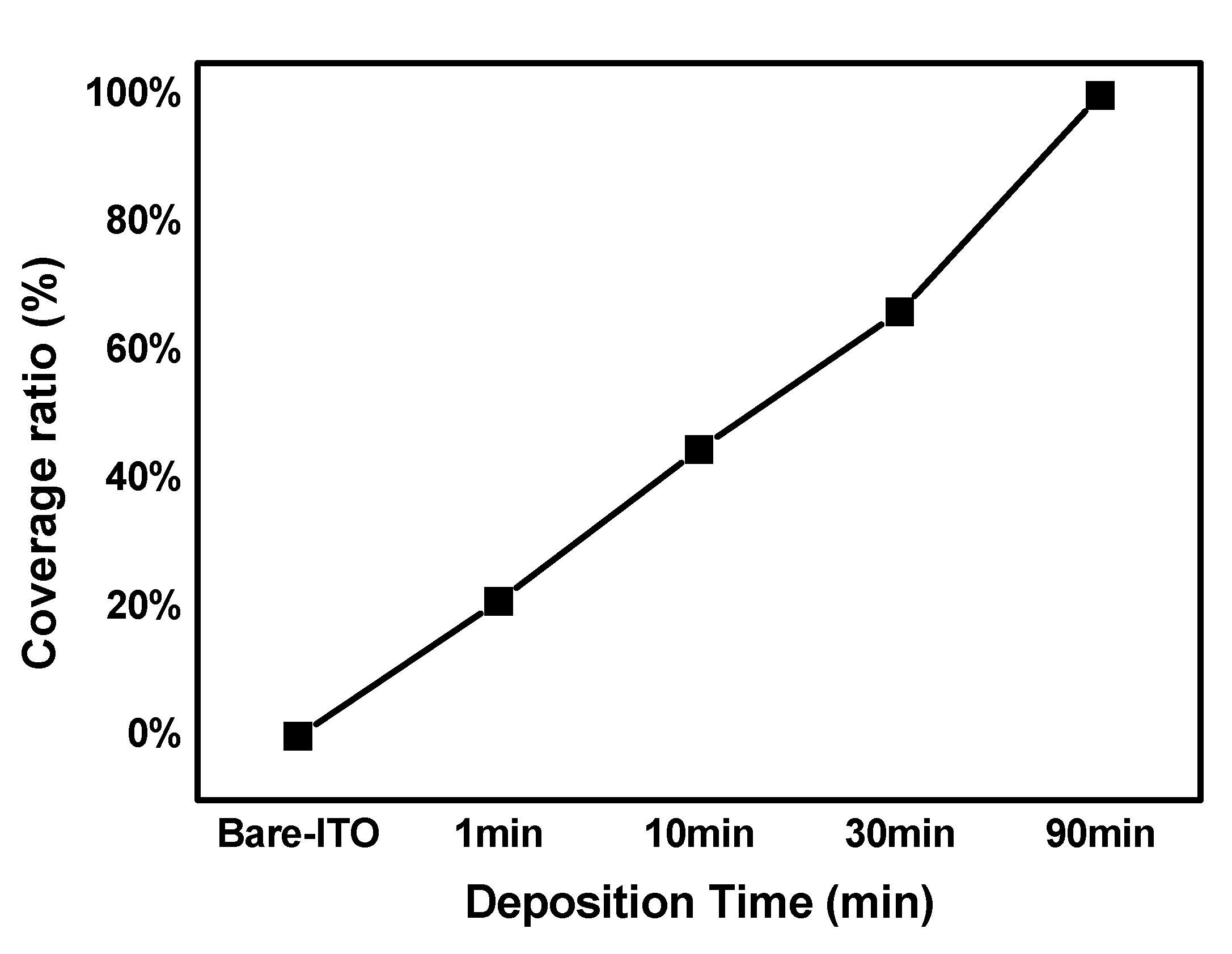
3. Results and Discussion

Once the SAM is present on the surface, the self-organization progresses in three phases. A low-density phase in which SAMs are randomly dispersed in the surface, an intermediate-density phase consisting of SAMs or disordered SAMs which are flat on the surface, and a high-density phase with close-packed order and SAMs standing normal to the surface [23]. Water plays a large role in the formation of SAMs. A thin water layer is typically present on the surface of hydrophilic silicon dioxide, and alkylsilane molecules physically adsorb to this water layer [24,25,26]. At this stage, the alkyl molecule is in a high flow state, similar to the equilibrium state. Before each molecule undergoes the condensation reaction, the SAM can be well positioned because of the strong van der Waals attraction generated between the alkyl chains of the CH3SAM molecule [27]. This van der Waals force is considerable because of the large surface area of the alkyl chain in the body part, as well as the contact part between the molecules. The physically adsorbed SAM is hydrolyzed when deposited at high temperatures, and hydrolysis converts the alkoxy groups to -OH groups [28]. The bonding part of CH3SAM proceeds with the dehydration/condensation reaction, with the adjacent -OH on the ITO substrate. Consequently, the bonding part of the SAM achieved complete chemical bonding with ITO substrate. The CH3SAM formation process is shown in Figure 2.
To confirm the changes of self-organization according to the different modification times of SAM on the surface of ITO, the devices were fabricated using gas phase method in which with CH3SAM was deposited on ITO at deposition times. These were labeled as Bare ITO, 1-min ITO, 10-min ITO, 30-min ITO, and 90-min ITO. Bare ITO and ITO/SAM surface wetness measured the contact angle to ensure that the SAM was effectively deposited on the ITO surface.
Figure 3 shows the contact angle for various CH3SAM deposition times at 120 °C on ITO. Contact angle measurement results were as follows: bare ITO, 57.41°; 1-min ITO, 63.43°; 10-min ITO, 73.76°; 30-min ITO, 81.47°; and 90-min ITO, 93.34°. The error ranges were: bare ITO, ±2.69°; 1-min ITO, ±3.07°; 10-min ITO, ±0.95°; 30-min ITO, ±0.51°; and 90-min ITO, ±0.23°. This result shows the low wettability characteristics of CH3SAM.
ITO is hydrophilic. However, the organic hole injection layer is hydrophobic, and this difference causes a heterojunction, which has a negative effect on the growth and stability of organic thin films [29]. Therefore, inserting the CH3SAM between the ITO and the HTM increases the hydrophobicity of the ITO surface, and eliminates the imbalance between the inorganic/organic interface at the ITO/HTL interface [30]. As shown in Figure 1, the terminal functional group in CH3SAM is a -CH3 group. Accordingly, the surface of the ITO is nonpolar and hydrophobic [21]. Note that the contact angle increased with increasing CH3SAM deposition time. This ratio can be confirmed using Cassie’s Law, as follows:
cos θ = ( 1 C 1 ) cos θ 1 + C 1 cos θ 2
In the above-stated equation, C_1 has a value between 0 and 1; θ is the contact angle of the modified CH3SAM on the ITO substrate; and θ1 is the contact angle of the bare ITO, while θ2 is the contact angle when CH3SAM is deposited for 90 min. According to Cassie’s Law, if CH3SAM is assumed to be 100% deposited on the surface of the 90 min deposition sample, it can be expressed as a percentage, i.e., as 0% for bare ITO, 21% for 1 min, 44.7% for 10 min, 66.2% for 30 min, and 100% for 90 min. Notably, as evident in the graph in Figure 4, the deposition time increases with an increase in the deposition time.
This simply indicates that CH3SAM was successfully adsorbed on the surface of the ITO as the deposition time increased, thereby causing the contact angle to increase. Figure 5 shows the atomic force microscopy (AFM) images of the bare ITO and 90-min ITO surfaces measured at 120 °C, and the root mean square of the average roughness values are as follows: bare ITO: 2.826 nm; 1-min ITO: 1.888 nm, 10-min ITO: 1.576 nm, and 90-min ITO: 1.339 nm.
These results confirm that the surface treatment method using SAM reduces the roughness of the ITO surface. In particular, it was confirmed that the surface roughness became lower as the SAM deposition time increased. Table 1 shows the roughness values according to the SAM deposition time. The deposition of CH3SAM over time on the ITO substrate revealed that the average roughness improved. These results consider that the ITO thin film is surface-treated with CH3SAM, which initially forms a disordered alignment of CH3SAM, which aligns well over time. The average roughness values of ITO bare and modified with a SAM are measured to be 1.418 nm, 1.139 nm, 1.240 nm, and 1.042 nm, respectively. To increase the hole injection efficiency of the OLED device, it is necessary to reduce the large energy level gap between ITO and the HTM.
The variation of ITO according to the deposition time of CH3SAM can improve the efficiency of porous injection between the anode and the HTM. Figure 6 shows the work function of bare ITO and CH3SAM deposited on the substrate for 90 min as measured through photoemission yield spectroscopy in air. The work function increased from 5.05–5.16 eV as CH3SAM was deposited on the ITO substrate. The results showed that the low work function of ITO substrates was easily controlled by the surface treatment of ITO substrates modified by CH3SAM. In other words, it is reported that large filling barriers between the ITO substrate and the HTM can be easily improved to facilitate carrier injection; thus helping to reduce drive voltage and enhance luminous efficiency.

4. Conclusions

Herein, we confirmed that the surface properties of the ITO can be changed by adjusting the CH3SAM deposition time. Furthermore, contact angle measurement showed that the ITO contact angle increased by 62.58% to 93.34° after the 90-min CH3SAM deposition, which was the highest value, with a contact angle of 57.41°. We also established that CH3SAM induced hydrophobic properties when deposited on the ITO surface. As the CH3SAM deposition time was gradually increased, the average roughness decreased by 51.6% to 1.399 nm for a deposition time of 90 min, compared to that of bare ITO, with an average roughness of 2.890 nm. In addition, the work function of the ITO surface was improved by approximately 0.11 eV by CH3SAM. These results showed that with increasing deposition time, disordered CH3SAM molecules were well aligned due to the van der Waals forces acting between the alkyl chain molecules. This demonstrates that CH3SAM is effectively deposited on the ITO surface as the deposition time increases, and the interfacial properties are improved.

Author Contributions

Conceptualization, S.-H.K.; methodology, J.-E.S.; validation, S.-G.P.; formal analysis, M.-G.B.; investigation, M.-G.B.; resources, D.-H.H.; data curation, M.-G.B.; writing—original draft preparation, M.-G.B.; writing—review and editing, S.-G.P.; visualization, M.-G.B.; supervision, S.-G.P.; project administration, H.-G.P.; funding acquisition, J.-E.S. All authors have read and agreed to the published version of the manuscript.

Funding

This work was supported by the Korea Institute of Energy Technology Evaluation and Planning (KETEP) and the Ministry of Trade, Industry & Energy (MOTIE) of the Republic of Korea (Project No. 20173010013680).

Conflicts of Interest

The authors declare no conflict of interest.

References

  1. Park, H.-G.; Park, S.-G. Electro-Optical Performance of Organic Thin-Film Using HAT (CN) 6 between Anode and Organic Materials. Coatings 2019, 9, 648. [Google Scholar] [CrossRef] [Green Version]
  2. Aleksandrova, M. Specifics and challenges to flexible organic light-emitting devices. Adv. Mater. Sci. Eng. 2016, 2016, 4081697. [Google Scholar] [CrossRef] [Green Version]
  3. Patel, B.N.; Prajapati, M.M. OLED: A modern display technology. Int. J. Sci. Res. Publ. 2014, 4, 1–5. [Google Scholar]
  4. Tseng, Z.-L.; Kao, P.-C.; Yang, C.-S.; Juang, Y.-D.; Chu, S.-Y. Transparent Al-doped ZnO anodes in organic light-emitting diodes investigated using a hole-only device. Appl. Surf. Sci. 2012, 261, 360–363. [Google Scholar] [CrossRef]
  5. Lee, B.J.; Kim, H.J.; Jeong, W.-I.; Kim, J.-J. A transparent conducting oxide as an efficient middle electrode for flexible organic tandem solar cells. Sol. Energy Mater. Sol. Cells 2010, 94, 542–546. [Google Scholar]
  6. Yu, S.-Y.; Huang, D.-C.; Chen, Y.-L.; Wu, K.-Y.; Tao, Y.-T. Approaching charge balance in organic light-emitting diodes by tuning charge injection barriers with mixed monolayers. Langmuir 2011, 28, 424–430. [Google Scholar] [CrossRef]
  7. Paramonov, P.; Paniagua, S.A.; Hotchkiss, P.J.; Jones, S.C.; Armstrong, N.R.; Marder, S.R.; Brédas, J.-L. Theoretical Characterization of the Indium Tin Oxide Surface and of Its Binding Sites for Adsorption of Phosphonic Acid Monolayers. Chem. Mater. 2008, 20, 5131–5133. [Google Scholar] [CrossRef]
  8. Brewer, P.J.; Lane, P.A.; Huang, J.; Demello, A.J.; Bradley, D.D.C.; Demello, J.C. Role of electron injection in polyfluorene-based light emitting diodes containing PEDOT:PSS. Phys. Rev. B 2005, 71, 205–209. [Google Scholar] [CrossRef]
  9. Lee, K.-S.; Lim, I.; Han, S.-H.; Kim, T.-W. Enhancement of the power efficiency for pin OLEDs containing organic p-type HAT-CN and n-type LCV materials. Org. Electr. 2014, 15, 343–347. [Google Scholar] [CrossRef]
  10. Lü, D.; Wu, Y.; Guo, J.; Lu, G.; Wang, Y.; Shen, J. Surface treatment of indium tin oxide by oxygen-plasma for organic light-emitting diodes. Mater. Sci. Eng. B 2003, 97, 141–144. [Google Scholar] [CrossRef]
  11. Ji, S.-B.; Choi, H.-W.; Yook, S.-K. Materials for Organic Light Emitting Diodes. Korean Ind. Chem. News 2016, 19, 1–11. [Google Scholar]
  12. Huang, Q.; Evmenenko, G.; Dutta, P.; Lee, P.; Armstrong, N.R.; Marks, T.J. Covalently Bound Hole-Injecting Nanostructures. Systematics of Molecular Architecture, Thickness, Saturation, and Electron-Blocking Characteristics on Organic Light-Emitting Diode Luminance, Turn-on Voltage, and Quantum Efficiency. J. Am. Chem. Soc. 2005, 127, 10227–10242. [Google Scholar] [CrossRef] [PubMed]
  13. Sung, M.-M. Self-Assembled Monolayers, SAMs. Electron. Mater. Lett. 2007, 3, 137–145. [Google Scholar]
  14. Ulman, A. Formation and Structure of Self-Assembled Monolayers. Chem. Rev. 1996, 96, 1533–1554. [Google Scholar] [CrossRef]
  15. Cayre, O.J.; Paunov, V.N. Fabrication of microlens arrays by gel trapping of self-assembled particle monolayers at the decane?—Water interface. J. Mater. Chem. 2004, 14, 3300. [Google Scholar] [CrossRef]
  16. Ramachandran, S.; Tsai, B.-L.; Blanco, M.; Chen, H.; Tang, Y.; Goddard, W.A. Self-Assembled Monolayer Mechanism for Corrosion Inhibition of Iron by Imidazolines. Langmuir 1996, 12, 6419–6428. [Google Scholar] [CrossRef]
  17. Andreatta, G.A.; Lachowicz, A.; Blondiaux, N.; Allebé, C.; Faes, A. Patterning solar cell metal grids on transparent conductive oxides using self-assembled phosphonic acid monolayers. Thin Solid Films 2019, 691, 137624. [Google Scholar] [CrossRef] [Green Version]
  18. Hillebrandt, H.; Tanaka, M. Electrochemical Characterization of Self-Assembled Alkylsiloxane Monolayers on Indium-Tin Oxide (ITO) Semiconductor Electrodes. J. Phys. Chem. B 2001, 105, 4270–4276. [Google Scholar] [CrossRef]
  19. Ashur, I.; Jones, A.K. Immobilization of azurin with retention of its native electrochemical properties at alkylsilane self-assembled monolayer modified indium tin oxide. Electrochim. Acta 2012, 85, 169–174. [Google Scholar] [CrossRef]
  20. Chi, Y.S.; Kang, S.M.; Choi, I.S. Surface Engineering Based on Self-Assembled Monolayers. Polym. Sci. Technol. 2006, 17, 172–181. [Google Scholar]
  21. Yan, L.; Huck, W.T.S.; Whitesides, G.M. Self-Assembled Monolayers (SAMs) and Synthesis of Planar Micro- and Nanostructures. J. Macromol. Sci. Part C 2004, 44, 175–206. [Google Scholar] [CrossRef]
  22. Zhao, Y.; Duan, L.; Zhang, D.; Dong, G.; Qiao, J.; Wang, L.; Qiu, Y. Systematic Investigation of Surface Modification by Organosiloxane Self-Assembled on Indium–Tin Oxide for Improved Hole Injection in Organic Light-Emitting Diodes. ACS Appl. Mater. Interfaces 2014, 6, 4570–4577. [Google Scholar] [CrossRef]
  23. Schwartz, D.K. Mechanisms and kinetics of self-assembled monolayer formation. Ann. Rev. Phys. Chem. 2001, 52, 107–137. [Google Scholar] [CrossRef]
  24. Wasserman, S.R.; Tao, Y.T.; Whitesides, G.M. Structure and reactivity of alkylsiloxane monolayers formed by reaction of alkyltrichlorosilanes on silicon substrates. Langmuir 1989, 5, 1074–1087. [Google Scholar] [CrossRef]
  25. Silberzan, P.; Leger, L.; Ausserré, D.; Benattar, J.J. Silanation of silica surfaces. A new method of constructing pure or mixed monolayers. Langmuir 1991, 7, 1647–1651. [Google Scholar] [CrossRef]
  26. Allara, D.L.; Parikh, A.N.; Rondelez, F. Evidence for a Unique Chain Organization in Long Chain Silane Monolayers Deposited on Two Widely Different Solid Substrates. Langmuir 1995, 11, 2357–2360. [Google Scholar] [CrossRef]
  27. Kim, H.R.; Kim, T.; Park, S. Effective hole-injection characteristics of organic light-emitting diodes due to fluorinated self-assembled monolayer embedded as a buffer layer. Polym. Int. 2019, 68, 1478–1483. [Google Scholar] [CrossRef]
  28. Aswal, D.; Lenfant, S.; Guérin, D.; Yakhmi, J.V.; Vuillaume, D. Self assembled monolayers on silicon for molecular electronics. Anal. Chim. Acta 2006, 568, 84–108. [Google Scholar] [CrossRef]
  29. Donley, C.L.; Dunphy, D.R.; Doherty, W.J.; Zangmeister, R.; Drager, A.S.; O’Brien, D.F.; Saavedra, S.S.; Armstrong, N.R. Indium—Tin Oxide Organic Interfaces; American Chemical Society (ACS): Washington, DC, USA, 2003; Volume 844, pp. 133–153. [Google Scholar]
  30. Wu, Q.-H. Progress in Modification of Indium-Tin Oxide/Organic Interfaces for Organic Light-Emitting Diodes. Crit. Rev. Solid State Mater. Sci. 2013, 38, 318–352. [Google Scholar] [CrossRef]
Figure 1. Molecular structure of n-decyltrimethoxysilane.
Crystals 10 00645 g001
Figure 2. n-decyltrimethoxysilane formation of process. SAM is formed through physisorption, hydrolysis, covalent grafting to the substrate, and in plane reticulation.
Crystals 10 00645 g002
Figure 3. Contact angle measurement of SAMs on ITO. (a) bare ITO (b) 1-min ITO (c) 10-min ITO, and (d) 30-min ITO (e) 90-min ITO.
Crystals 10 00645 g003
Figure 4. Coverage ratio calculated using Cassie’s Law.
Crystals 10 00645 g004
Figure 5. AFM 3D image (a) bare ITO, and (b) SAM 90-min ITO. The AFM images and roughness (c) bare ITO (d) 1-min ITO (e) 10-min ITO, and (f) 90-min ITO.
Crystals 10 00645 g005
Figure 6. Square root of the photoemission yield.
Crystals 10 00645 g006
Table 1. Results of the roughness values when surface treatment was performed, according to the SAM deposition time. (Mean–Mean line; Rpv–R peak to peak value, Rq–R root mean square, and Ra–R average Rz–ten point height).
TimeMinMaxMidMeanRpvRqRaRz
Bare ITO−8.05139.03515.4920.00047.0862.8261.41846.349
1 min−6.83135.61314.3910.00042.4441.8881.13941.707
10 min−8.3809.7970.7090.00018.1771.5761.24017.001
90 min−9.1987.193−1.0020.00016.3911.3391.04214.560

