1. Introduction
Optogenetics is the combination of genetic and optical methods aimed at achieving gain or loss of specific functions or events in defined cells of living tissues [
1]. This technology integrates genetic control tools targeted at specific cells responsive to light, together with technologies designed to deliver controlled illumination to the targeted investigation sites. Currently, the primary cell types studied are those of the nervous system, responsible for signal transmission between different areas of the body and the coordination of voluntary and involuntary actions.
Optogenetics employs light-activated proteins (opsins) to control neuronal functions, thus becoming an evolving methodology in neuroscience seeking deeper understanding of the neurological system. Optogenetic techniques activate or inhibit distinct neuronal populations with unprecedented precision in spatial, temporal, and neurochemical terms. It is the only available method capable of activating specific neuronal populations embedded in dense, heterogeneous structures within milliseconds [
2].
The human brain comprises approximately 86 billion neurons. Each neuron consists of two main parts: a central region containing the nucleus, known as the soma, and numerous thin tubes radiating from the central region called neurites, which are subdivided into axons and dendrites [
3]. Neurons connect to each other through synapses, forming a complex interconnected network called the neural network. This network has a significant capacity for processing and storing information.
The nervous system, a complex set of neurons, communicates through pulses or action potentials transmitted through synapses. Electrical synapses transmit signals through rapid variations in sodium and potassium ion concentrations. An action potential fired by a presynaptic neuron generates a pulse transmitted to postsynaptic neurons, influencing the likelihood of these neurons firing their action potentials. These potentials must summate, either spatially or temporally, to reach the threshold for action potential initiation [
4].
Neuronal behavior often encounters failures due to genetic malformations or degenerative diseases affecting proper nervous system functionality. Optogenetics emerges with tools facilitating the study of neuronal network behaviors by precisely activating or inhibiting certain neuronal populations. Neuronal cells generally lack efficient natural response to light stimuli, necessitating artificial sensitization through opsins—light-sensitive membrane proteins acting as ion channels. Each opsin responds selectively to specific wavelengths, allowing particular ions to pass, modulating neuronal activity [
5].
Commonly used opsins include microbial types such as ChR2 (channelrhodopsin-2), VChR1 (volvox-channelrhodopsin-1), and NpHR (halorhodopsin), typically delivered to neurons using viral vectors. Once neurons express these opsins, optical tools installed appropriately stimulate neurons via direct illumination. Additionally, acquiring local biopotentials is crucial to analyzing optical stimulation efficacy. Each opsin type has a specific peak activation at different wavelengths. For instance, a 500 nm wavelength yields a 50% relative response for ChR2, 70% for VChR1, and 25% for NpHR [
6].
Various optogenetic instrumentation technologies have evolved to facilitate targeted cell stimulation and response measurement effectively. Tools primarily involve benchtop lasers delivering optimal power and wavelengths via optical fibers. Wireless technologies have shown promise in reducing animal stress and expanding behavioral study possibilities. One example is the use of a wireless interface with two LED-fiber optic optrodes for neuronal excitation [
7]. Recognizing optogenetics’ importance, Nature Methods selected it as the 2010 method of the year, highlighting significant interdisciplinary growth potential [
8].
Optical neural interfaces have evolved significantly with the integration of light-based stimulation and neural signal recording. Recent work has demonstrated various microfabricated optrode platforms capable of simultaneously stimulating and recording neural activity [
9,
10,
11]. These include wireless head-mounted systems and multi-channel micro-LED stimulators integrated into silicon chips, validating the potential for bidirectional and mobile neuromodulation. Flexible and scalable implant architectures with embedded light sources and detectors are also enabling large-area cortical interfacing and real-time fluorescence imaging [
12].
Artifact reduction remains a critical challenge in combined optogenetic and electrophysiological systems. Material innovations, such as PEDOT:PSS coatings on graphene electrodes, have been shown to suppress light-induced artifacts during stimulation [
13]. Complementarily, simulation-driven models have predicted interference-free spike detection frequencies, and novel concepts such as lithium niobate microring resonators are being investigated as purely optical extracellular voltage sensors [
14].
Hybrid sensors combining optical fibers with piezoelectric films have demonstrated mechano-electrical conversion for physiological sensing, offering alternative signal acquisition modes for implantable interfaces [
15]. Complementary technologies, such as bio-impedance feedback-controlled drilling systems, are improving the precision and safety of implant placement during neurosurgery [
16].
Outside neural interfaces, fiber-optic optrodes are being applied in environmental and chemical sensing. SERS-active fiber tips with plasmonic nanostructures have achieved detection limits in the nanomolar range for analytes such as crystal violet, opening applications in trace-level diagnostics and pollutant monitoring [
17,
18]. Photonic crystal hydrogels and in situ porous polymer tips have similarly enhanced the detection of heavy metals and pesticides in microfluidic systems [
19].
In toxicology, oxygen-sensitive optrodes have been used to detect metabolic changes in fish embryos in response to pollutants, offering fast and non-invasive physiological readouts [
18,
20]. These optrodes have also been employed in bioreactor systems to quantify gas–liquid mass transfer efficiency. Meanwhile, engineered microbes have been monitored via optrodes with fluorescence detection capabilities, enabling real-time biosensing even in opaque or complex media [
19]. This has extended into bioelectronic platforms where CMOS chips interact with light-responsive living cells to close the loop between biological input and optoelectronic output [
20].
Together, these developments demonstrate the growing versatility of optrodes across disciplines. By converging optics, microfabrication, and biology, these tools are pushing the boundaries of neural engineering, biosensing, and diagnostic technologies.
Currently, however, applications remain limited to specialized laboratory environments equipped with complex, bulky, and expensive instruments. There is an increasing demand for compact, intelligent, interconnected, and cost-effective devices across various fields, suggesting wider adoption of these technologies. Integrating this trend with optogenetics enhances accessibility and encourages neuroscientific research, elucidating brain behavior under normal, pathological, or situational conditions and identifying particular neuronal networks and their roles. Translational research, especially in rodents, aims to understand brain behavior using precise temporal and spatial optogenetic control. All current solutions rely on commercial components, limiting genuine miniaturization.
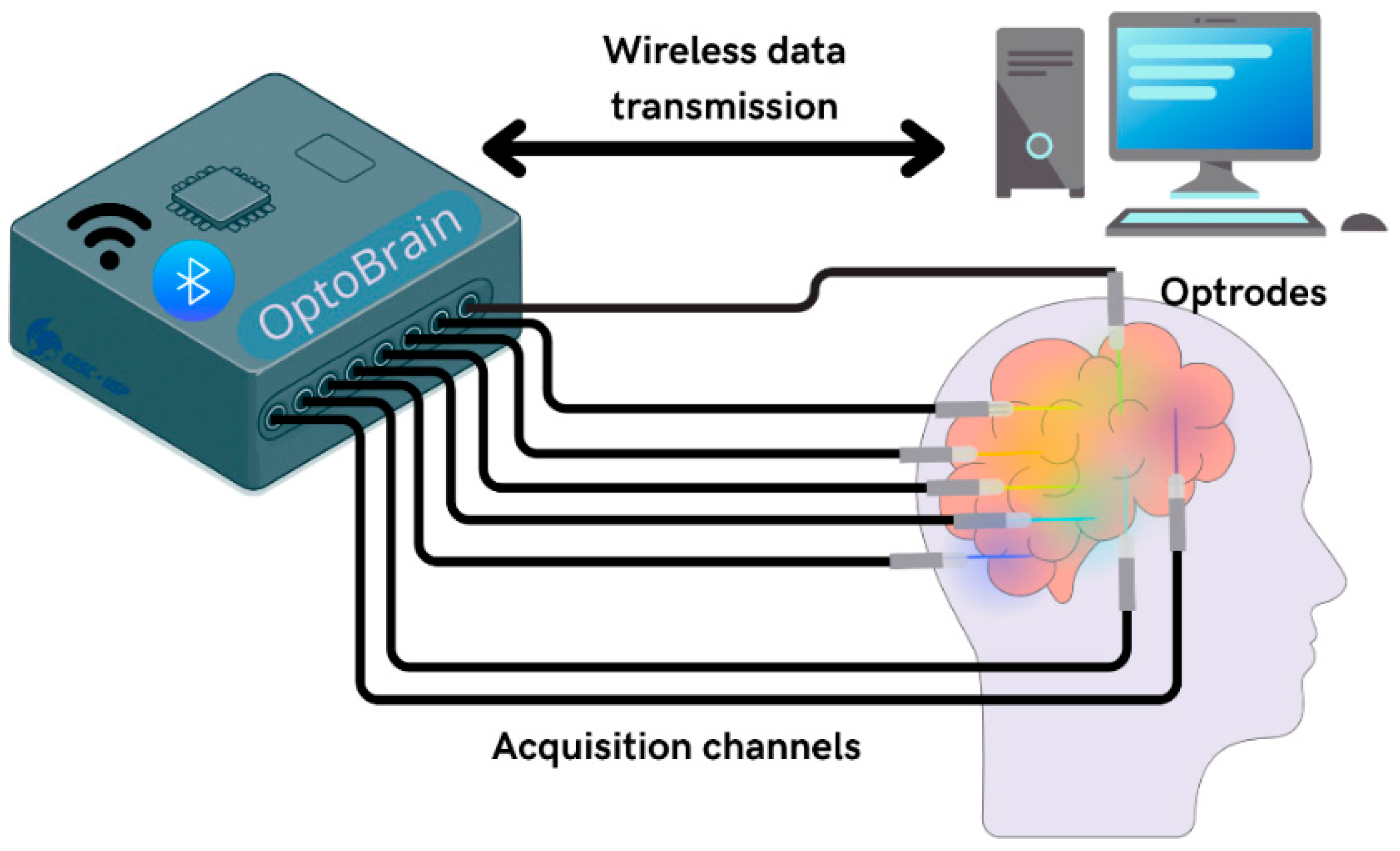
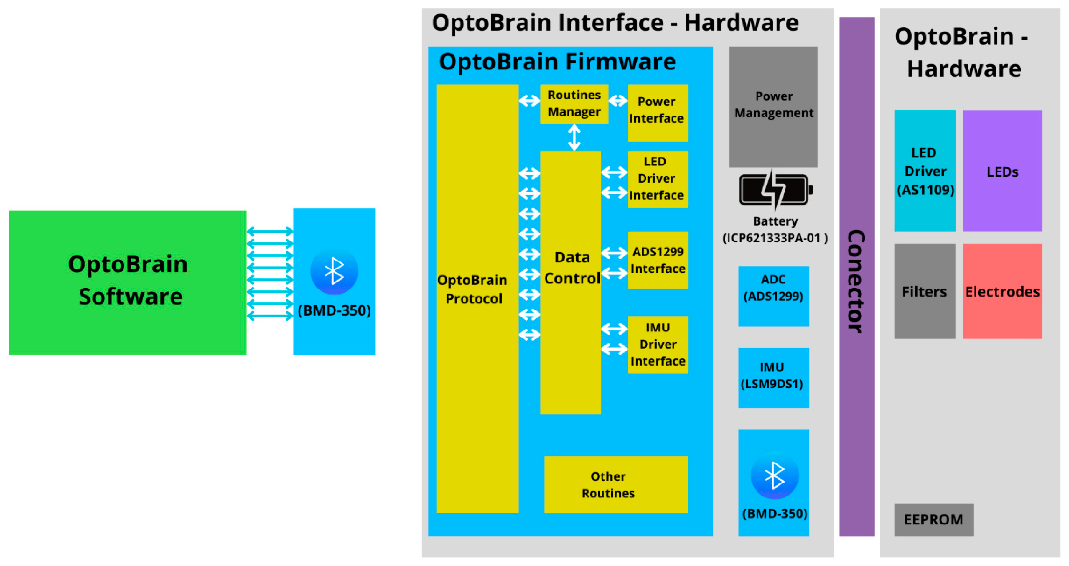
This paper introduces OptoBrain, a comprehensive and portable wireless system designed for optogenetic applications, integrating modules for data acquisition, signal processing, control, and neurostimulation. The overall OptoBrain system application is represented in
Figure 1.
The main innovation presented in this paper is the development of multi-channel interfaces for acquisition of neurological signals, facilitating the creation of ultra-compact, low-power, and cost-effective optogenetic devices. The OptoBrain system has the potential to advance novel treatment techniques, stimulate growth in the medical instrumentation market, and foster the training of new professionals across various disciplines, including medicine, biology, and technical fields. Furthermore, its progressive adoption and the utilization of its electronic modules, optrodes, and open-interface architectures are expected to lead to substantial long-term cost savings. This work validates OptoBrain from an engineering standpoint. Biological validation (in vitro or in vivo) remains as future work and is outside the scope of this manuscript but the system was extensively tested and validated in a laboratorial engineering environment. To achieve these objectives, the OptoBrain development was guided by specific technical requirements: miniaturization for compact form factor suitable for small animal models, power efficiency enabling multi-hour experiments on single battery charge, reliable wireless performance supporting multi-channel neural recording without packet loss, cost-effectiveness to promote research laboratory adoption, and modular architecture allowing custom optrode configurations for diverse experimental protocols.
3. Evaluation Methodology
3.1. Energy Consumption Profile
The analysis of the energy consumption profile is extremely important to identify any abnormal power usage and to estimate the device’s battery life under various conditions. Therefore, different usage profiles were defined so that immediate current draw, power consumption, total energy used, and system autonomy can be measured.
The list below describes common scenarios characterized by their theoretical power consumption:
Standby—The Bluetooth module is advertising (ready to connect to another system), but no data are being acquired via the ADS1299 or inertial sensor, and no LEDs are activated.
ADS1299 Data Acquisition—Similar to Standby, but with the ADS1299 running in four different configurations:
- a.
1 channel at 250 samples per second (sps);
- b.
8 channels at 250 sps;
- c.
1 channel at 20,000 sps;
- d.
8 channels at 2000 sps.
ADS1299 Data Read and Transmission—The ADS1299 is actively sampling, and the data are being sent via Bluetooth, under the same configurations as scenario 2.
Inertial Sensor Active—The IMU is powered and streaming data (in addition to the conditions of scenario 3, for example).
Optical Stimulation Active—One or more LEDs are activated at maximum intensity (in addition to the data acquisition and wireless transmission of scenario 3).
For each of the above profiles, the immediate current draw was measured, and from that the power consumption and the estimated runtime of the 240 mAh battery were calculated. An auxiliary board was used to read the voltage and current, calculate the power consumption and register the acquired data into a CSV file. The power calculated is the mean value and the energy consumption is the product of the mean power by the time of operation.
For some profiles, some estimates were made using data from the datasheets of the components:
CPU current: 3.7 mA;
Bluetooth receiver current: 5.4 mA;
Bluetooth transceiver current: 7.5 mA;
Average ADS1299 current: 7.14 mA (analog) plus 1 mA (digital) = 8.14 mA;
IMU current: 4.6 mA.
An additional test protocol for analyzing noise in the power supply was proposed during the pilot trials of the board, because it was noticed that there was noise, which could have originated from the power rails, during some analog acquisitions. Thus, a specific test was devised to evaluate the noise on the power supply lines under different conditions. In this test, various power supply topologies were used to power a resistor divider connected directly to one channel of the ADS1299, in order to adjust the input level to a suitable range for analog reading. The following supply configurations were tested, whose scenarios are illustrated in
Figure 4:
VIN with −2.5 V (using the negative supply rail as reference);
+3.3 V with −2.5 V;
±2.5 V (dual supply);
External battery with −2.5 V;
External battery with GND as reference.
Figure 4.
The five power supply topologies tested to characterize the influence of noise.
Figure 4.
The five power supply topologies tested to characterize the influence of noise.
These topologies consider different types of power sources that could be used to power the sensors. Because the interface can be connected to external sensors (such as pressure sensors), which depend on an input excitation voltage, any noise on the input supply can translate into noise on the sensors’ signals. The analysis performed in this case consisted of finding the highest amplitudes and frequencies of these noise components via FFT (Fast Fourier Transform) analysis and comparing the noise levels among the topologies.
3.2. Analog Acquisition Test Setup
The OptoBrain signal acquisition is performed by the ADS1299 module, which has very well-defined noise characteristics provided by the manufacturer, which indicate that performance related to noise can be optimized by simply adjusting the data reading frequency and the programmable amplifier gain. Decreasing the acquisition frequency increases the average time over which each reading is taken, making the reading more stable and less susceptible to input noise compared to faster readings. On the other hand, increasing the amplification gain reduces the effect of input-referred noise. Nevertheless, every real-world component introduces noise related to the amplification and acquisition process. Therefore, quantifying the noise during analog signal acquisition is fundamental to understanding whether it impacts the desired signal measurement. For performing input noise tests, each differential channel under evaluation must be shorted. Data were collected for 10 s for the specific gains and sampling rates below:
Gains: 1, 2, 4, 8, 12 and 24 V/V;
Sampling rates: 250, 500, 1000 and 2000 samples per second.
These values were transmitted to a computer in real time using the Bluetooth dongle. Higher sampling rates were not used due to throughput limitations during the tests. For input noise measurement, all sample points during the 10 s of collection were considered to ensure at least 1000 samples. The maximum and minimum values within this window were used for peak-to-peak (µVpp) calculation, and the RMS value (µVRMS) was calculated from the standard deviation of the entire set of points. To allow the comparison, the same noise-related parameters provided by the ADS1299 datasheet were used:
The ADS1299 manufacturer provides well-described tables with noise values captured by its converter, as well as formulas for calculating the parameters. For the OptoBrain board, a comparative table was made against the values available in the datasheet, as well as noise graphs over time and in histogram format.
To measure the offset and its variation with respect to gain, the inputs of all eight channels were short-circuited. Simultaneous acquisitions on all eight channels were performed for 3 to 4 s for each gain, starting from 1 to 24 V/V, with a sampling rate of 250 Hz. The comparison between the average values for each channel/gain allows understanding the behavior of the initial DC level of each input. To measure the gain variation between the ADS1299 channels, the same constant voltage of 0.15 V was applied to six of the channels (channels 2 and 8 were excluded as they showed instability in their operation). This voltage value was chosen so that a gain of 24 V/V would not saturate the amplifier. Subsequently, the voltage levels for each gain were analyzed. For this test, the signal was divided by the gain value. To calculate the gain deviation between the channels, the case where the gain is 24 V/V was used for comparison, as this is the case where the offset has the least influence. The parameter used was the percentage deviation of a given channel (
Vi) relative to the first channel (
V1):
The value considered at the end was the maximum deviation. This test protocol aims to investigate potential interference or crosstalk between the different subsystems of the device. Specifically, it tests whether the operation of one component (such as the radio transmitter or the LED driver for optogenetics) introduces noise or artifacts into the signals of another component (such as the analog biopotential readings). One part of this test involved operating the LED driver (AS1109) at full load (turning LEDs on and off at maximum current) while recording from the ADS1299 channels. Any coincident disturbances in the recorded signals would suggest electromagnetic or ground interference caused by the LED switching. Another part involved intensive Bluetooth activity (forcing continuous data transmission bursts) while observing the analog signal baseline for anomalies. Additionally, scenarios were created where the inertial module was actively communicating over I2C/SPI to assess if digital bus noise leaked into the analog front-end.
The test procedure was designed to compare signal recordings in conditions with and without active potential interference sources. If needed, measures like adding shielding, altering grounding schemes, or adjusting firmware scheduling would be considered based on the findings. For acquisition, the sampling rate was configured at 2000 samples per second, with a gain of 1 V/V, allowing the maximum excursion of the input voltage. To measure the rejection to interference between channels (crosstalk), the following formula was used:
where
crosstalk(
x,
y) represents the interference that channel
y suffers from channel
x, in dB,
Vix is the amplitude of the first harmonic in the frequency spectrum of channel
x, and
Voy is the amplitude of the largest harmonic among the first 10 of the signal in channel
y.
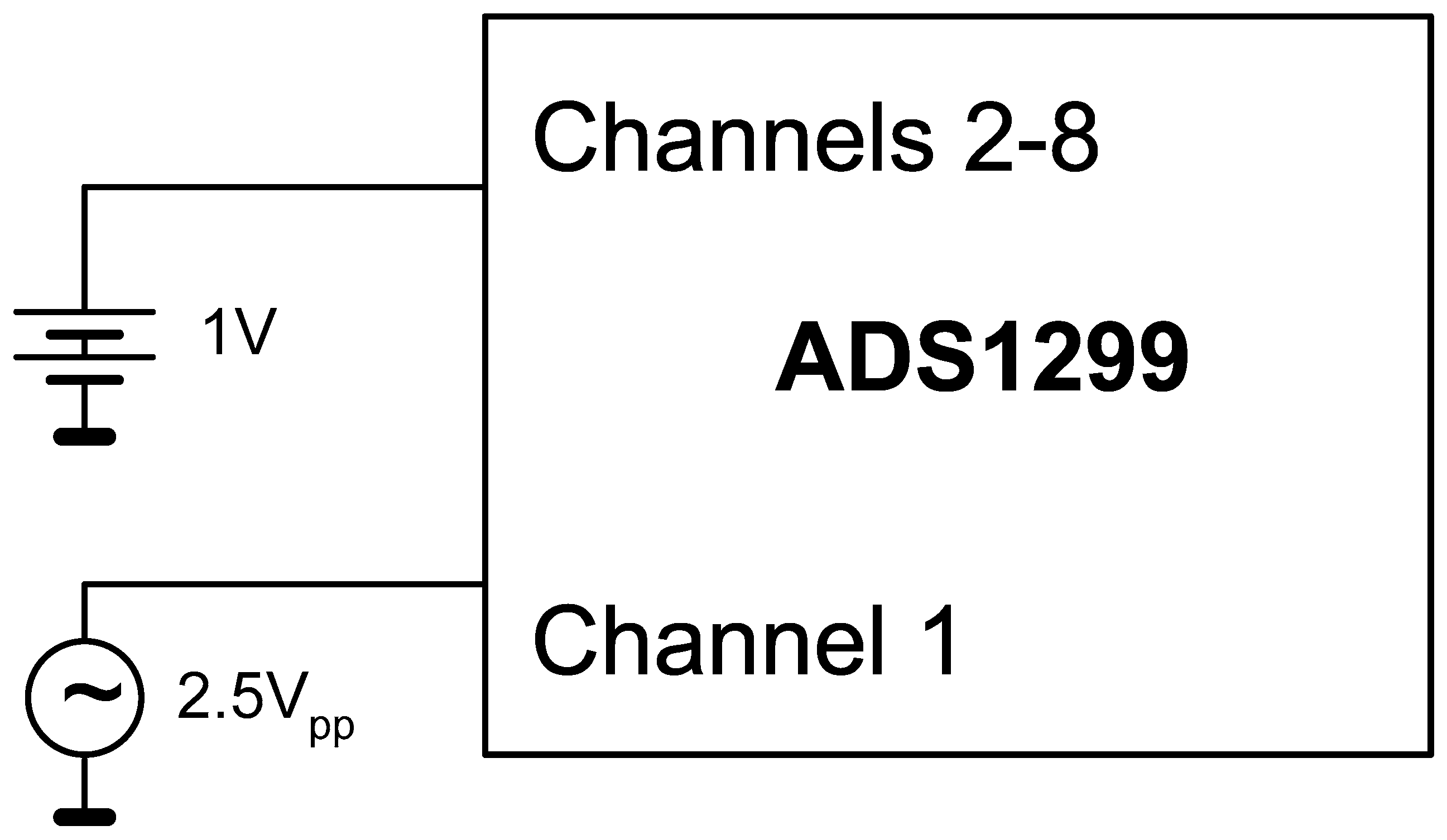
Figure 5 shows the test setup diagram for crosstalk analysis.
3.3. Frequency and Linearity Profile
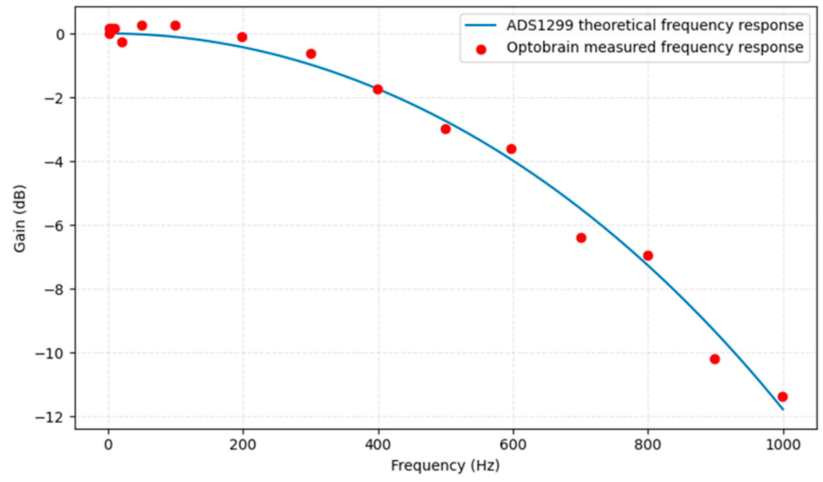
The frequency characterization and linearity analysis of the OptoBrain system are essential to ensure that the system is compatible with the envisioned optogenetic application. The ADS1299 datasheet does not mention any notch filters or configurable input filters. However, it presents a decimation filter, which is linked to the system’s acquisition. To avoid aliasing in the data acquisition, third-order sinc filters are used. To analyze the system’s behavior for this type of filter, some tests were performed, as documented below, with the goal of obtaining the frequency spectrum for the ADS1299 decimation filter. For this purpose, a sinusoidal wave of approximately 1.6 V was applied to channel 1, with a gain of 1 V/V. The sampling rate was 2000 sps, to obtain the largest possible spectrum. The sine wave frequency should vary from 1 Hz to 1 kHz. For each frequency, a 10 s data acquisition should be performed. After collecting all signals, the magnitude spectrum in frequency was calculated for each signal to obtain the frequency and amplitude. The amplitude of the 1 Hz signal was used as a reference for gain calculation, which was performed by dividing the amplitude of the signal in a given frequency (from the FFT analysis) by the amplitude of the 1 Hz component.
This test protocol was intended to verify the linearity of the signal acquisition across the entire input range. Linearity in this context means that the output digital value is directly proportional to the input voltage over the full scale of the ADC, without significant deviation. To test this, a series of DC voltages spanning from near 0 V up to the ADC’s reference voltage (full-scale range) were applied to an ADS1299 input channel. For each input value, the corresponding output code from the ADC was recorded. Additionally, some negative voltages (down to the negative reference limit, since the ADS1299 can measure bipolar signals when biased at mid-supply) were applied to test linearity in the negative range as well.
These input–output pairs were then plotted and fitted to a straight line. The primary metric for linearity is how closely the data points follow a linear fit, typically quantified by the R2 coefficient or by the maximum deviation in percent of full scale. If the system is perfectly linear, the points form a straight line with slope corresponding to the ADC gain and intercept point corresponding to the offset (which was separately tested in the offset analysis). By conducting this test on all channels, we also ensured there were no channel-specific nonlinearities introduced by any analog components or calibration mismatches.
3.4. Wireless Transmission Profile
To evaluate the ability of the OptoBrain system to transfer data wirelessly, the throughput of the Bluetooth link and the reliability of data transfer are key factors. The test setup for the wireless communication involved the OptoBrain interface transmitting data to the receiver dongle, while a packet sniffer (with Nordic’s firmware and the Wireshark software version 3.6.0) captured the Bluetooth packets. The throughput was measured by analyzing the size of data packets and their arrival times. In addition to raw throughput, this protocol tested data integrity by comparing transmitted data versus received data to ensure no corruption. For instance, sequence number counters were included in the data payload so that any lost or out-of-order packets could be detected on the receiving end. Finally, the wireless range was informally tested by increasing the distance between the OptoBrain device and the receiver to determine at what point communication became unreliable. Although range was not the primary focus (since experiments are expected to be within a few meters), it was useful to confirm that typical lab distances did not pose a problem.
4. Experimental Results
4.1. Energy Consumption and Power Supply Noise Analysis
The measurements for each defined usage profile provided insights into the Interface’s battery performance and helped identify any unexpected power draw. In standby mode, the current draw was on the order of 12 mA, indicating that the system can remain idle for extended periods with negligible battery drain. Activating the ADS1299 acquisition increased the consumption in proportion to the number of channels and the sampling rate: for instance, running 8 channels at 2000 sps drew 25 mA, which is significantly more current than 1 channel at 250 sps, which drew 14 mA. This increase in current is expected. When data transmission via Bluetooth was added, the current increases to 29 mA. Even though the current is higher with all channels and the data transmission, the system was still able to operate for several hours on battery in this mode.
By combining the measured current draws with the battery capacity, we estimated the system’s autonomy for each scenario. In a typical use case (for example, 8 channels sampling at 250 sps with continuous Bluetooth transmission), the 240 mAh battery would last for about 3 h with an 80 mA current consumption. This meets the requirements, since optogenetic experiments are usually shorter than this duration. In less demanding scenarios (fewer channels or intermittent transmission), the battery life is correspondingly longer, potentially exceeding 5–6 h for a 40 mA current consumption.
No irregular power consumption was observed beyond the planned profiles—each component (ADS1299, IMU, LEDs, Bluetooth) contributed to the overall consumption as anticipated. This confirms that there are no hidden power drains in the system. The consumption profile analysis also highlighted which modes are most taxing (simultaneous high-speed sampling and LED activation), allowing us to optimize usage or provide guidelines (for example, using duty cycles for LED stimulation to conserve energy). In summary, the system’s power consumption aligns with expectations, and the measured profiles affirm that the interface can support the intended experimental use cases on a single battery charge.
For each power supply connection topology at the ADS1299 input referred to in
Figure 4, graphs of the acquisition over time and frequency (from FFT analysis) are presented below, as well as a table comparing the amplitude of the main noise components of each topology.
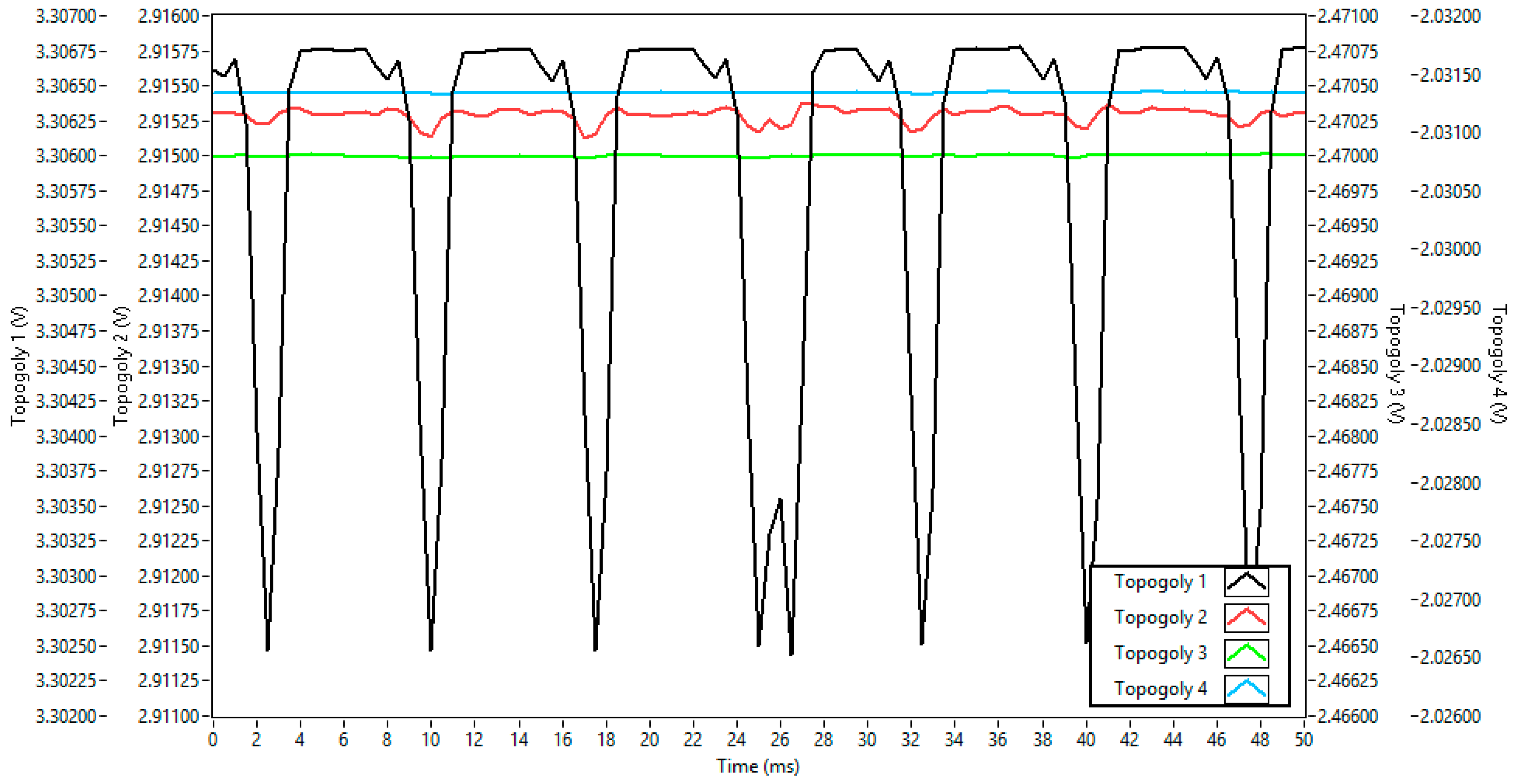
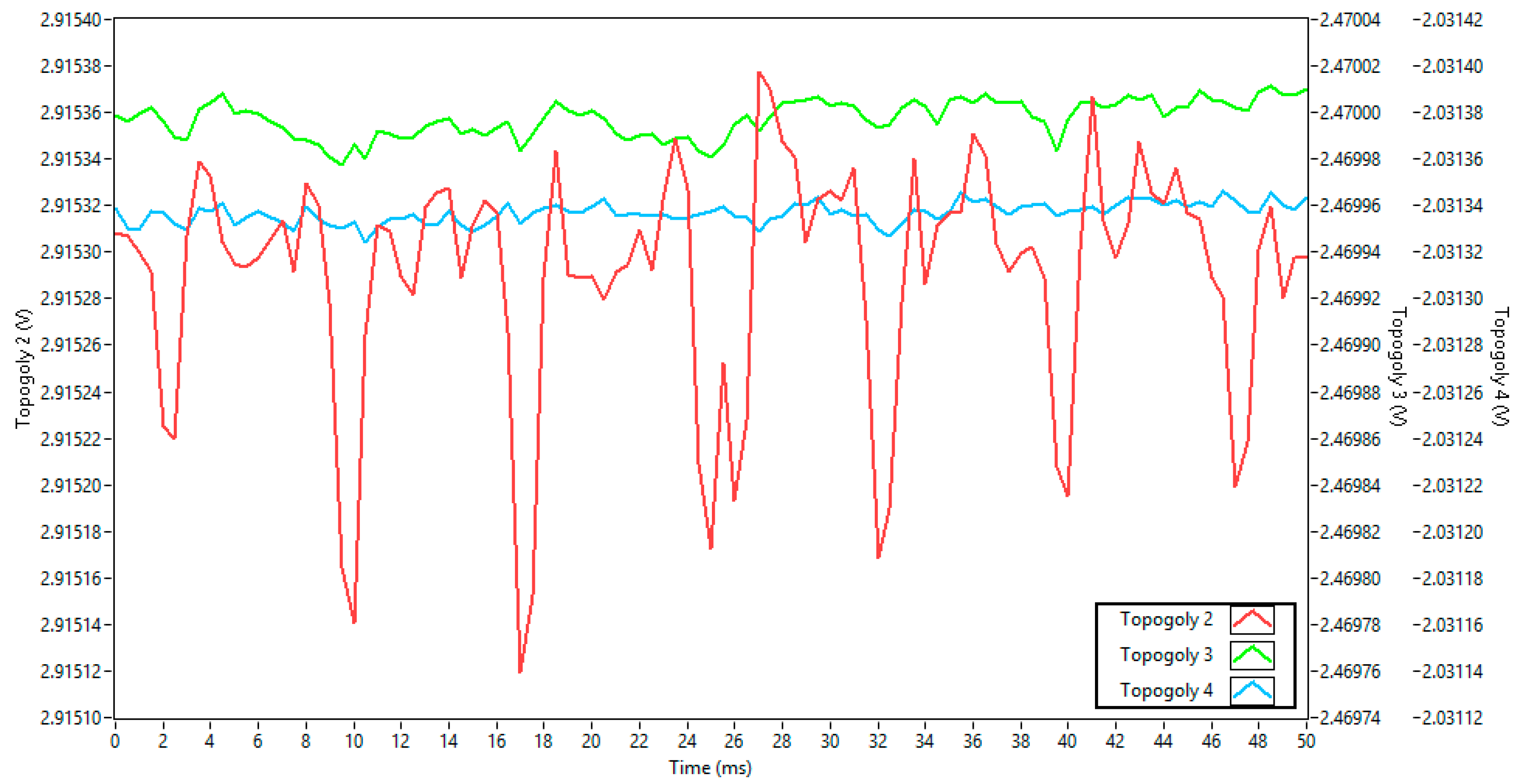
Figure 6 compares the effect of noise from each type of power supply when connected directly to the inputs through a voltage divider for the first four topologies. Containing approximately 100 points, each channel had its
y-axis adjusted in level but maintained the same 5 mV delta for each of the channels, so their intensities could be visually compared. To visually understand the proportionality of noise influence among the topologies,
Figure 7 shows topologies 2, 3, and 4 with an axis interval fixed at 0.3 mV, an interval 16 times smaller than the peak-to-peak interval axis that encompasses topology 1 in
Figure 6.
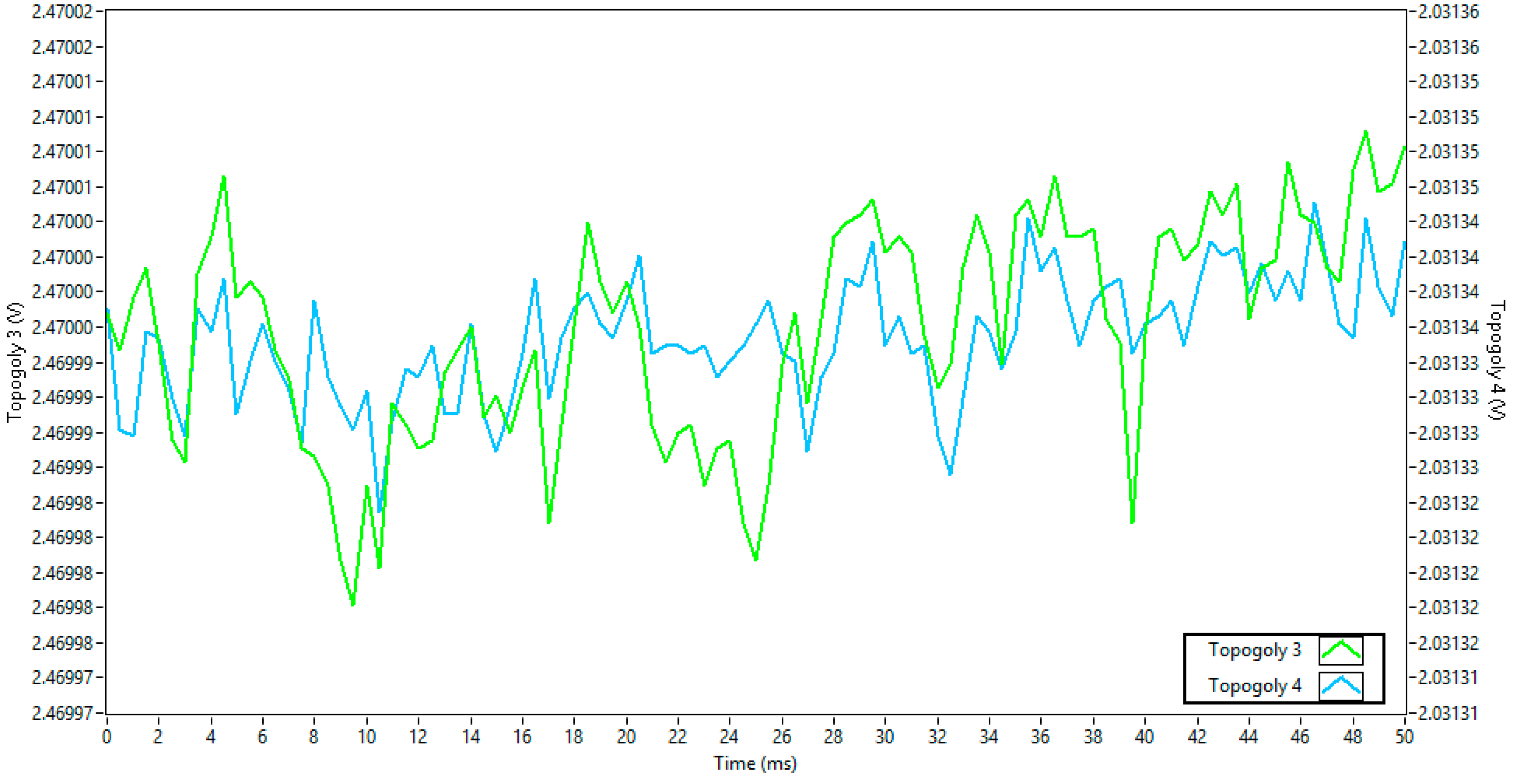
Figure 8 compares the power supply noise for topologies 3 and 4, with a
y-axis interval of 50 µV, about 6 times smaller than topology 2 in peak-to-peak values.
Finally, a separate power supply noise measurement was made for topology 5, which also used topology 5 of the OptoBrain interface.
Figure 9 shows the time series with a 50 ms window. The peak-to-peak amplitude seen in the graph is approximately 20 µV, 40% lower when compared to topology 4 and 250 times lower than topology 1.
These results clearly demonstrate that the power source choice significantly affects noise levels. Topology 1, which used the board’s main battery input (VIN), introduced the most significant noise. In contrast, topology 5, which used a separate external battery with a ground reference, provided the cleanest power, with a peak-to-peak noise amplitude approximately 250 times lower than the worst-case scenario.
Table 1 depicts the RMS noise value for each topology.
This meets the requirements, as this duration is sufficient to accommodate common optogenetic stimulation protocols, which can range, for example, from 15 min daily [
27] sessions to continuous 60 min experiments [
28].
4.2. Analog Acquisition Analysis
The characterization of the input noise floor was accomplished by analyzing data recorded with all inputs shorted to ground. The measured noise level was extremely low—on the order of a few microvolts peak-to-peak. This is in line with the ADS1299 specifications and confirms that the front-end electronics introduce minimal noise. The noise appeared as a very slight random fluctuation around zero, with no discernible bias or drift. The amplitude of this mains frequency component was, however, negligible (well below 1 μV RMS), indicating effective shielding and filtering. No other significant spectral lines were present, confirming the absence of unexpected interference.
The system’s intrinsic noise floor is very low and does not limit the device’s ability to detect the small biopotential signals of interest. The input noise remains within acceptable bounds across different gain settings and operational modes, giving confidence that the measurements reflect the true physiological signals rather than internal noise.
For almost all 120 measurements performed across the four sampling rates within the six different gains, the measured noise value and the parameters calculated based on these measurements were better than or equal to those provided in the ADS1299 datasheet. Only seven specific peak-to-peak noise values were greater than those described in the datasheet. This is likely because this noise measurement was made with respect to the entire 10 s sample of each collection, unlike the datasheet recommendation of taking just 1000 samples, which increases the possibility of capturing less common noises of higher amplitudes.
Table 2,
Table 3,
Table 4,
Table 5,
Table 6 and
Table 7 depict the measured values and reference values measured for the input noise.
Table 8 shows the offset variation in the OptoBrain board varying channel and gain. The offset and gain verification tests indicate that the system’s measurements are accurate and consistent with the expected values. In terms of DC offset, when the inputs were shorted to ground, the ADC outputs fluctuated around zero with no significant fixed offset; the average value was within a few microvolts of zero. When a small DC voltage was applied (e.g., 5 mV), the readings reflected that value, with an error of less than ±0.01 mV, which is negligible. This demonstrates an excellent zero-offset performance.
Table 9 lists the analysis of the effect of gain on output voltage for each channel. Regarding gain accuracy, the system showed a high degree of linearity. For a reference 1.00 mV peak input signal, the measured amplitude across the digitized data was about 0.99 mV peak, corresponding to a gain error of roughly −1%. Across a range of test amplitudes (from 0.5 mV up to 10 mV), the output-to-input relationship remained linear (R
2~0.999) and the gain error never exceeded 1–2% of the full-scale value. This small error can be calibrated out if needed, but it is already within the tolerance of the application. Tests were conducted at an ambient laboratory temperature of approximately 26.8 °C. The board’s supply voltage was provided by a lithium battery and is not considered a critical parameter for this test, as internal regulators provide stable power to the analog-to-digital converter.
In practical terms, these results mean that the interface can accurately capture the true amplitude of biopotential signals and that any minor systematic errors in offset or gain are very small. The linear response also implies that the device does not introduce distortion, so signal waveforms are preserved in shape. Overall, the offset is virtually zero and the gain is very close to unity (within calibration limits), confirming that the hardware design and calibration are effective.
It is noted that the voltages tend to stabilize as the gain increases, varying considerably between gains 1 and 2 compared to the others. The ADS1299 showed distinct offset values for each channel. This variation is small and can be corrected by software calibration. Regarding gain, the maximum deviation between channels was 0.1% (seen between channels 1 and 5). This deviation is less than the 0.2% full-scale specified in the datasheet.
For DC inputs,
Table 10 shows the results of the common mode rejection ratio (CMRR) measurements and calculations considering the three applied voltage levels:
V1 = 0.2 V,
V2 = 2 V, and
V3 = 3.8 V. A small increase in the absolute CMRR value with gain 24 was observed, compared to gain 1. This increase was 14.72 dB considering
V1 and
V2, and 6.60 dB considering
V2 and
V3.
For AC inputs,
Table 11 shows the results for input frequencies between 1 Hz and 100 Hz, with sampling rates varying from 250 to 2000 samples per second.
Regarding the variation in CMRR with sampling rate, there was no significant variation (less than 2.5%). In all cases, the CMRR was better than −116 dB. According to the ADS1299 datasheet, the CMRR varies between −110 and −120 dB, so a greater CMRR attends to the specifications.
For some cases of the 1 Hz test, there were no peaks representing the components in the frequency spectrum. In this case, the noise level was considered as amplitude, causing the final value in the interference to increase.
Table 12 shows the result of interference between channels (crosstalk) when the input signal was 1 Hz with a gain of 1 V/V. Channels 2 and 8 were not included in the tests because they exhibited abnormal behavior, likely due to degradation in their internal amplification stages or other components in the acquisition chain of these channels that may have occurred between experiments. Consequently, reliable measurements could no longer be obtained for these specific channels in the subsequent tests. It is expected that the performance of these channels would be similar to that of the others, since they share the same circuit architecture and components.
For the 2 Hz interference frequency and 1 V/V gain, the FFT components were above the noise, especially the second harmonic (4 Hz).
Table 13 shows the result of interference between channels when the input signal was 2 Hz with a gain of 1 V/V.
A variability between channels is observed. Some reached a higher interference (−97 dB) for channels adjacent to the input channel, but except for these cases, all other channels showed interference less than −110 dB, which is specified by the datasheet.
Table 14 shows the result of interference between channels when the input signal was 10 Hz with a gain of 1 V/V.
For the test with a gain change of 2 V/V, a smaller amplitude (1.2 V) was adjusted in the function generator to achieve a high amplitude without saturating the amplifier.
Table 15 shows the result of interference between channels when the input signal was 10 Hz with a gain of 2 V/V.
The ADS1299 datasheet provides a crosstalk value of −110 dB. Most of the measurements extrapolated this value, excluding the 1 Hz and 1 V/V results, as in most cases it was difficult to find interference at that frequency. However, it is noted that there is greater interference between channels 3 and 4 and between channels 5 and 6. This could be caused by several factors, such as closer proximity between the wires connected to these channels, but this hypothesis was discarded by repeating the tests with the wires arranged to maximize separation. The hypotheses that the PCB the trace routing could have caused this crosstalk was also discarded. For these reasons, it is understood that there is likely greater internal interference between these channels within the ADS1299. A support ticket was sent to the manufacturer to understand the cause of this interference. In any case, a 100 dB crosstalk rejection represents an attenuation of 100,000 times in the interference signal, while a 91 dB rejection represents 35,000 times. Therefore, it is not recommended to apply AC signals with this order of magnitude of amplitude difference simultaneously on these channels.
The interference tests revealed that the system’s design successfully minimizes crosstalk and noise coupling between subsystems. When the optical driver was activated (with LEDs switching at high current), the ADS1299 recorded signals showed only a very minor transient synchronous with the LED pulses—on the order of a few microvolts—and only on channels physically closest to the LED wiring. This small artifact is considered negligible for most purposes, but indicates that careful routing and perhaps additional filtering could eliminate entirely even this minor effect. Importantly, the artifact was consistent and predictable, meaning it could also be subtracted or ignored if necessary.
4.3. Frequency Response Evaluation
Figure 10 shows the gain (in dB) of the ADS1299 input in the frequency domain. This frequency response evaluation showed that the system’s analog front-end has a flat gain (±0.1 dB) from DC up to approximately 200 Hz, after which a gentle roll-off begins. The –3 dB point was observed around 400 Hz. This behavior is in line with design expectations, considering the ADS1299’s built-in digital filter settings and any small analog RC filters on the inputs.
No unexpected resonant peaks or irregularities were present in the response curve, indicating that the analog input network is stable and well-behaved across frequencies. The flat response in the relevant bandwidth (up to a few hundred hertz for neural signals) means the interface does not distort or diminish the physiological signals of interest. In summary, the bandwidth of the system is more than sufficient for capturing the necessary signal content, and the observed roll-off at high frequencies serves to filter out unwanted high-frequency noise, which is beneficial.
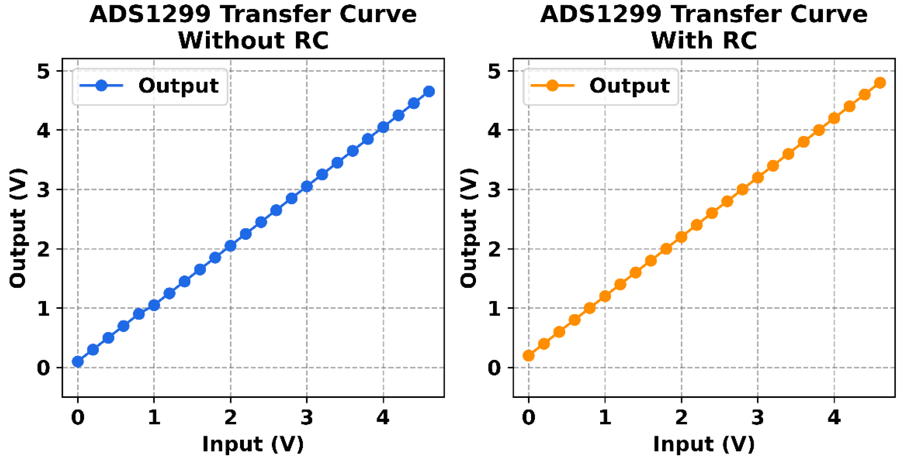
Figure 11 shows the linearity curves without and with the use of RC filters. As can be observed, the system demonstrated excellent linearity across the tested input voltage range. When plotting the ADC output values against the known input voltages, the resulting graph was essentially a straight line. The coefficient of determination (R
2) was above 0.9999, indicating virtually perfect linear correlation. The maximum deviation from the ideal line (after accounting for the tiny offset error discussed earlier) was on the order of 0.5% at the extreme ends of the range, very close to the specified ADS1299 integral nonlinearity. In practical terms, this means if we apply 100% of the input range, the worst-case deviation was around 0.5% of that value, and for most mid-range values the error was even smaller. No individual channel showed any peculiar deviation; all behaved uniformly, which reflects good matching in the analog front-end and proper calibration. The linearity holds in both the positive and negative input directions—the response was symmetric. In conclusion, the acquisition system’s linearity is confirmed to be within specifications, assuring that the amplitude of signals is measured accurately throughout the dynamic range and that the system does not introduce distortion even when signals approach the upper limit of values the ADC can digitize.
Knowing the input impedance of the analog front-end is crucial, as it should be high enough to avoid loading the biological signal sources. According to the ADS1299 datasheet, the input DC impedance is greater than 1 GΩ. To verify this, a test was conducted using a precision multimeter (NI PXI-4071) [
29] capable of measuring up to 5 GΩ. In this test protocol, each ADS1299 input channel (referenced to the common ground) was measured individually. The interface was powered on, and no signal was actively driven into the channel (inputs were left floating or connected through a very large resistor). The multimeter was connected to measure the resistance from the input node to ground over a period of about 10 s, and the average value was noted. Because the datasheet provides only DC impedance values, no frequency-dependent impedance measurement was performed; the focus was solely on the DC input impedance. The test ensures that the hardware (including any protection circuits or filters on the input) does not significantly lower the impedance from the ideal value stated by the ADC.
All measured channels showed an impedance above 1 GΩ (in many cases, the readings were at the limit of the multimeter’s range, indicating it could be even higher), confirming that each analog input has an extremely high impedance. This means the interface’s inputs draw virtually no current from the signal source, which is an ideal scenario for biopotential measurements, where source impedances (like electrode-skin interfaces) can be high. No channel exhibited a markedly lower impedance than the others, which implies that all input protection and filtering components were correctly chosen and are not loading the inputs appreciably. This uniformly observed high impedance across channels validates that the design (which uses the ADS1299’s high-impedance instrumentation amplifiers and appropriate biasing networks) is functioning as intended. In practical terms, such a high input impedance ensures that connecting the OptoBrain interface to electrodes or sensors does not alter the signals. Even if an electrode has an impedance of, for example, 100 kΩ, the higher than 1 GΩ input impedance means less than 0.01% of the signal is dropped across the electrode, which is negligible. Thus, from the perspective of signal fidelity and safety, the interface’s input impedance is more than sufficient.
4.4. Wireless Transmission Evaluation
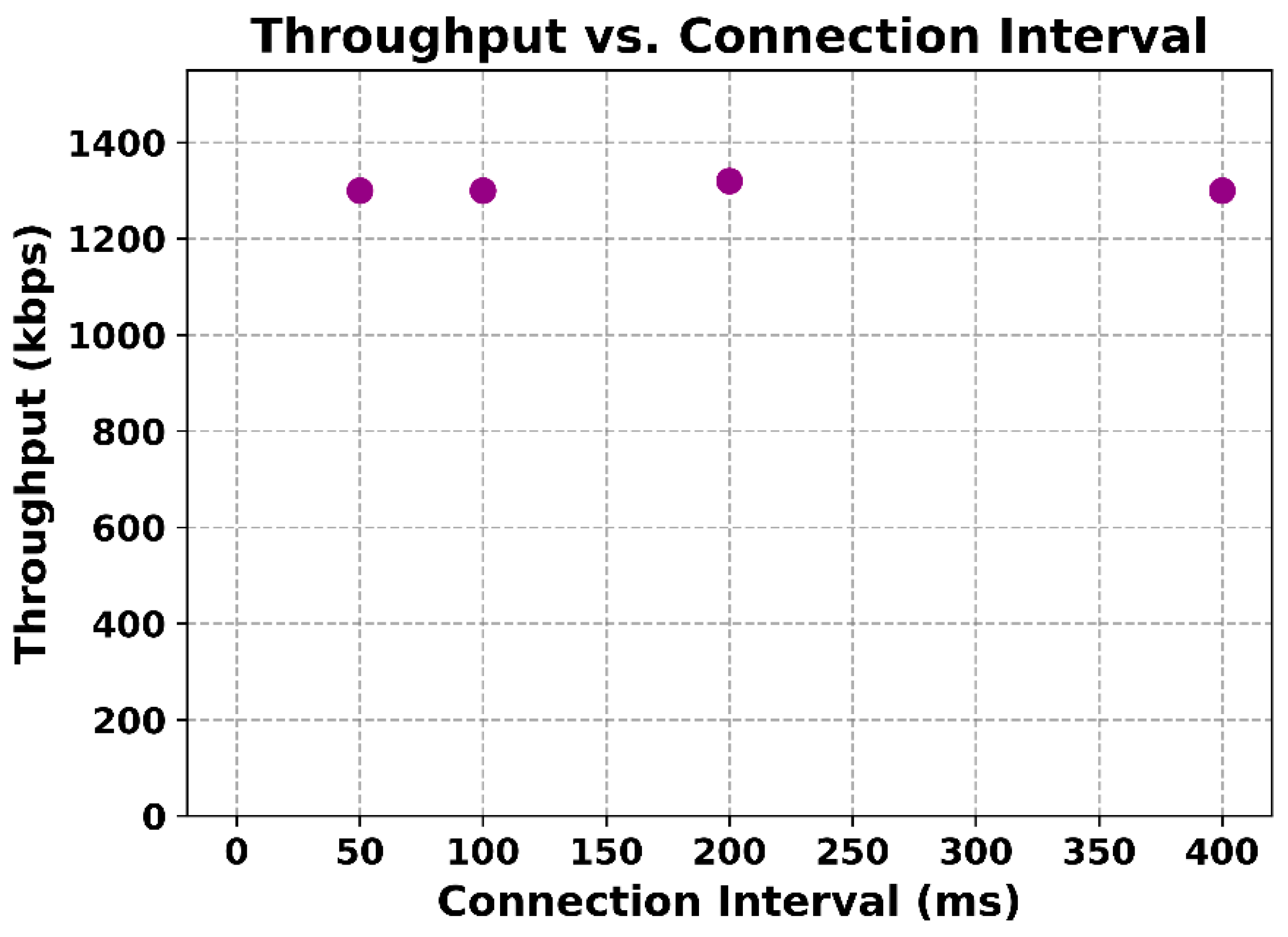
The wireless data transmission tests yielded very positive results. The Bluetooth Low Energy link was able to handle the continuous streaming of data from the device without any packet loss under normal operating conditions. The maximum stable throughput observed was roughly 1300 kbps, which corresponds to the data from 8 channels at 2000 sps plus overhead. This agrees with the BLE theoretical maximum for the given connection parameters. Crucially, the data received matched exactly the data sent. Sequence number counters embedded in the packets showed no gaps or duplications, indicating that no packets were lost or reordered. Even when the device was at the far end of the lab (approximately 10 m away, with a clear line of sight), the connection remained reliable, and the throughput was unaffected. Only when additional physical obstructions or longer distances were introduced did the link quality begin to drop, as expected for BLE. During these tests, various data patterns were used (for example, streaming actual recorded physiological data versus synthetic test patterns), and it was found that the data content did not impact throughput or integrity. The BMD-350 module supports a theoretical maximum throughput of 1426 kbps under BLE 5 (2 M PHY, DLE). In our tests, stable throughput of ~400 kbps was measured, reflecting application-level performance including protocol overhead. Stress testing under interference and multi-device conditions will be explored in future work.
Figure 12 depicts the measured throughput (in kbps) as function of the BLE connection interval (in ms).
In summary, the OptoBrain interface’s wireless communication has been validated to meet the real-time requirements of optogenetic experiments. It can stream multi-channel high-resolution data while simultaneously receiving commands (such as those to trigger LED stimulation) with no noticeable lag. This successful wireless performance is a critical confirmation that the system can be used in freely moving animal experiments, providing both freedom of movement and dependable data capture.
5. Conclusions
This work successfully introduces OptoBrain, a novel, comprehensive, and portable wireless system specifically engineered for advanced optogenetic applications. The OptoBrain system was validated from an engineering standpoint. Biological validation (in vitro or in vivo) remains as future work and is outside the scope of this manuscript. By integrating modules for data acquisition, signal processing, control, and neurostimulation, OptoBrain addresses the critical need for compact, intelligent, interconnected, and cost-effective devices in neuroscientific research. A significant contribution of this research is the development of multi-channel interfaces for neurological signal acquisition, which facilitates the creation of ultra-compact, low-power, and cost-effective optogenetic devices. These selections underpin the system’s low power consumption, high data throughput, and multichannel capabilities. Cross-domain insights (e.g., extreme environment sensing, acoustic tomography) are valuable, though outside the scope of this work. These will be considered in future interdisciplinary extensions.
Table 16 and
Table 17 make a comparison of the characteristics of the proposed OptoBrain interface with selected commercial systems and similar systems found in the literature. It must be noted the nonexistence of electronic systems to implement solutions of closed-loop optogenetic stimulation, nor electronic system solutions providing a large simultaneous number of acquisition and stimulation channels as it is proposed with the OptoBrain.
Latency requirements for closed-loop neuromodulation vary widely depending on the target application: up to ~200 ms for motor BCIs [
39], ~0.5–1 s for seizure suppression [
40,
41], tens of milliseconds for oscillation modulation [
42], and <10 ms with sub-ms jitter for STDP [
43,
44]. In this work, no closed-loop experiments were performed. Based on throughput characterization, the estimated end-to-end delay is on the order of tens of milliseconds, which may already be compatible with several applications. However, systematic evaluation of latency, jitter, and stimulation artifacts remains a limitation of the present work and will be addressed in future studies. For latency-critical scenarios, we envision embedding the closed-loop controller directly in the firmware to reduce dependency on wireless transmission.
Experimental results confirm the robust performance of the OptoBrain system across various critical parameters. The energy consumption profile aligns with expectations, demonstrating efficient operation in standby, data acquisition, and transmission modes. The 240 mAh battery supports 2–3 h of continuous operation in demanding scenarios, extending to 5–6 h in less intensive use cases, which is adequate for most optogenetic experiments. Analysis of power supply noise revealed that while some topologies introduced minor interference, topology 5, utilizing an external battery with a ground reference, exhibited the lowest noise, with peak-to-peak amplitude approximately 250 times lower than topology 1.
The analog acquisition analysis demonstrated exceptionally low input noise, in the order of a few microvolts peak-to-peak, consistent with the ADS1299 datasheet specifications. The frequency spectrum of this intrinsic noise showed only negligible mains interference, confirming effective shielding. Offset and gain verification tests confirmed accurate and consistent measurements, with ADC outputs fluctuating around zero for shorted inputs and a maximum gain deviation between channels of 0.1%, which is within datasheet specifications. Common-mode rejection ratio (CMRR) measurements consistently exceeded the ADS1299 datasheet specifications, indicating strong rejection of common-mode interference. While some inter-channel crosstalk was observed, particularly between channels 3 and 4, and 5 and 6, most instances were below −110 dB, aligning with datasheet values, suggesting potential internal interference within the ADS1299 in specific adjacent channels. Crosstalk was observed between channels Ch3–Ch4 and Ch5–Ch6, likely due to PCB trace coupling and ADS1299 internal architecture. Firmware-based subtraction and hardware shielding are potential mitigation strategies, to be developed in future work.
The frequency response evaluation confirmed a flat gain (±0.1 dB) from DC up to approximately 500 Hz, with a −3 dB point around 1.2 kHz, ensuring accurate capture of relevant neural signals without distortion. Linearity tests yielded excellent results with an R2 value above 0.9999, signifying a nearly perfect linear correlation between input voltage and output digital values across the entire dynamic range. Furthermore, the input impedance measurements confirmed an extremely high impedance (above 1 GΩ) across all analog inputs, preventing loading of biological signal sources and ensuring signal fidelity.
Finally, the wireless transmission tests demonstrated robust performance, achieving a stable throughput of approximately 400 kbps without packet loss under normal operating conditions. Data integrity was maintained, and the wireless link remained strong even at distances of 10 m, confirming the system’s suitability for freely moving animal experiments. By adopting BLE 5.0, OptoBrain can integrate into distributed wireless ecosystems, supporting IoT-based neuroscience frameworks.
In conclusion, OptoBrain represents a significant step towards more accessible and versatile optogenetic research. Its compact, low-power, and high-performance design, coupled with validated wireless capabilities, positions it as a valuable tool for advancing our understanding of neural circuit function in both normal and pathological states.

