
Simulation Study of Silicon-Based Single-Photon Avalanche Diodes with Double Buried Layers and Deep Trench Electrodes

Abstract
:1. Introduction
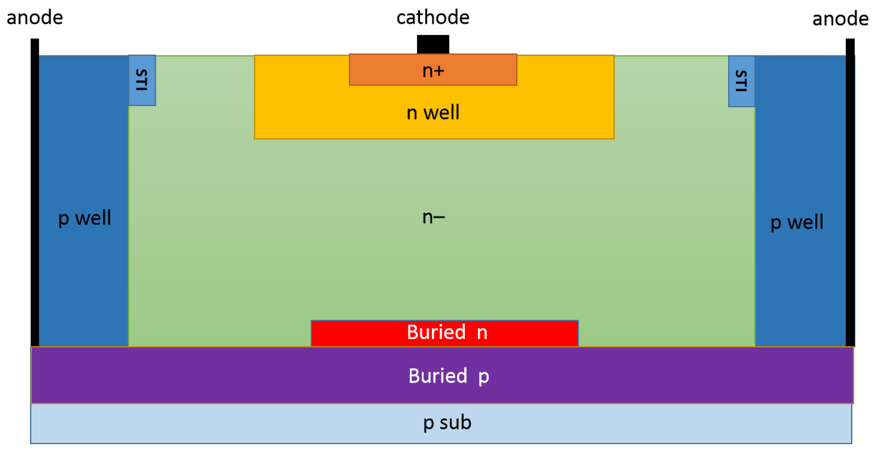
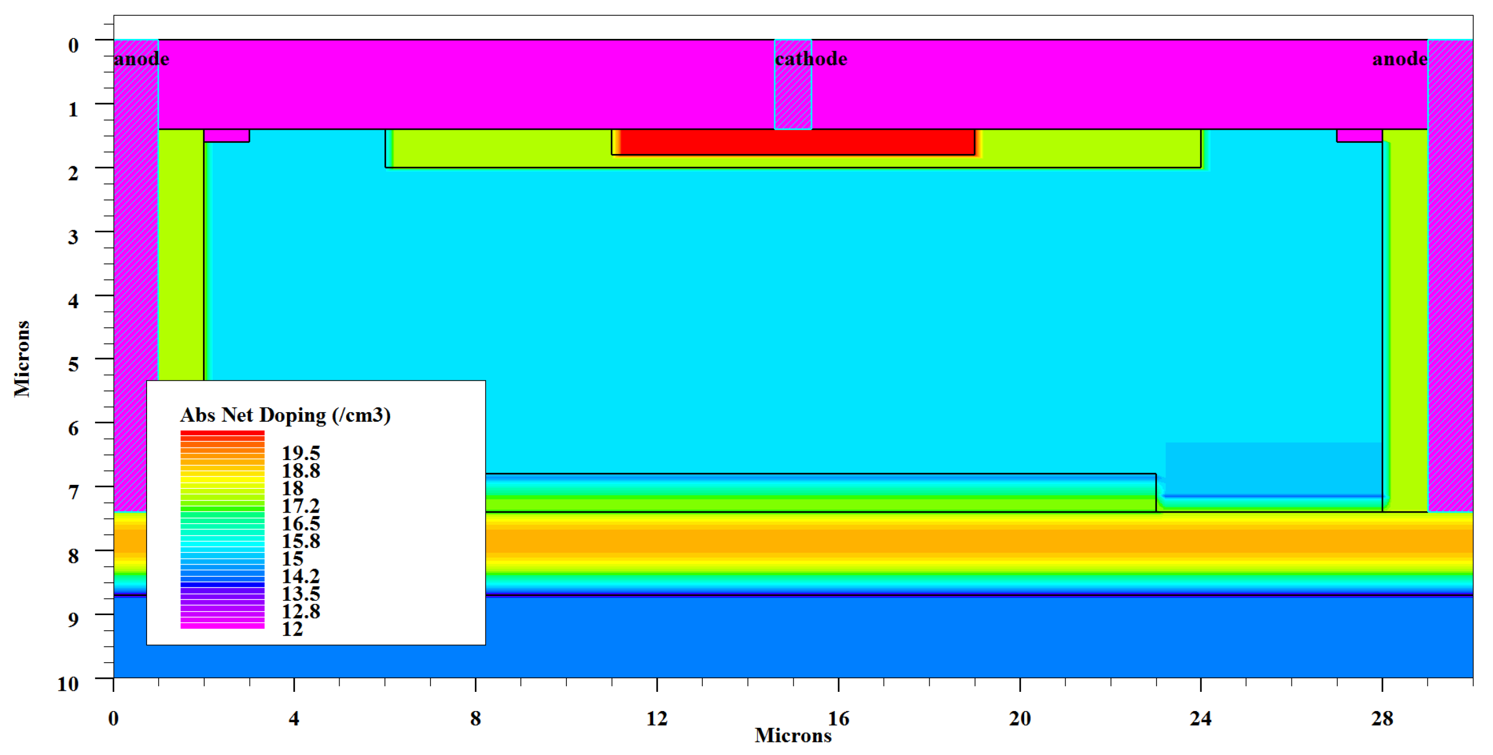
2. Simulations
3. Result and Discussion
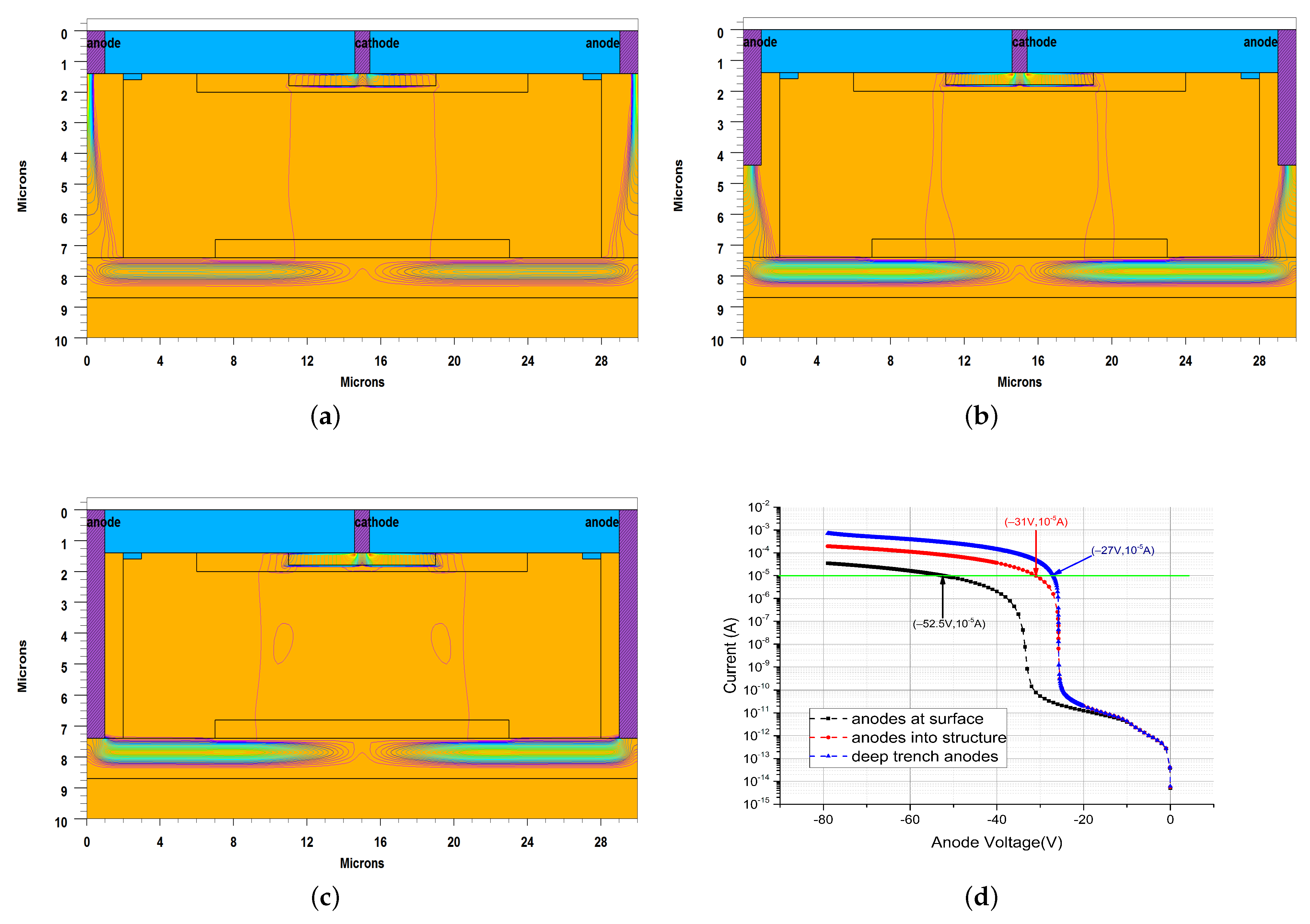
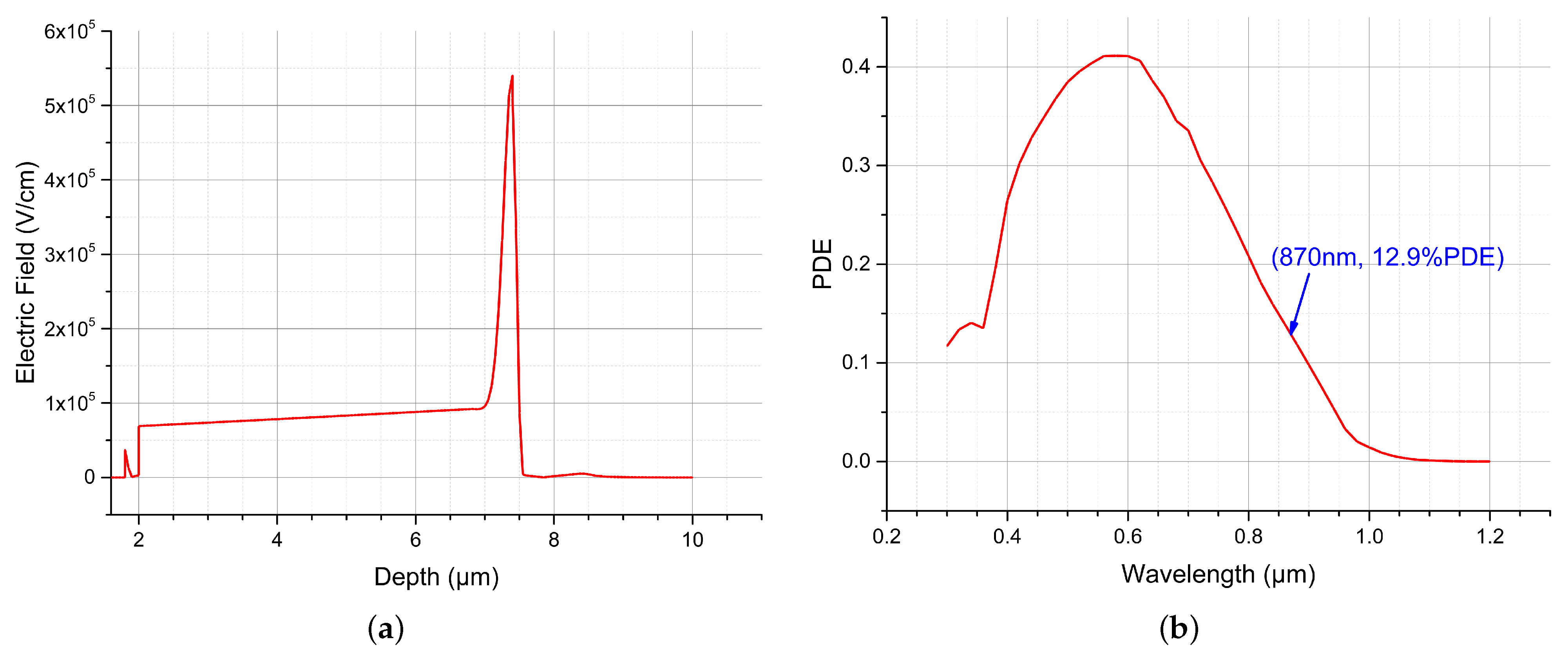
3.1. Deep Trench Anode
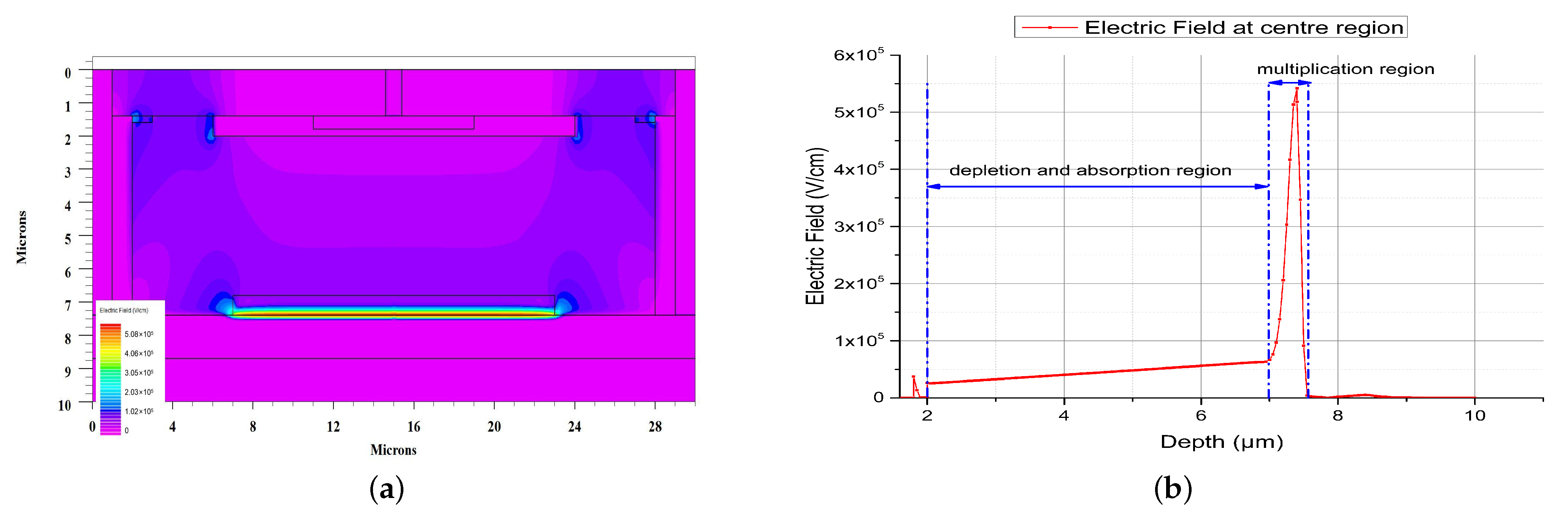
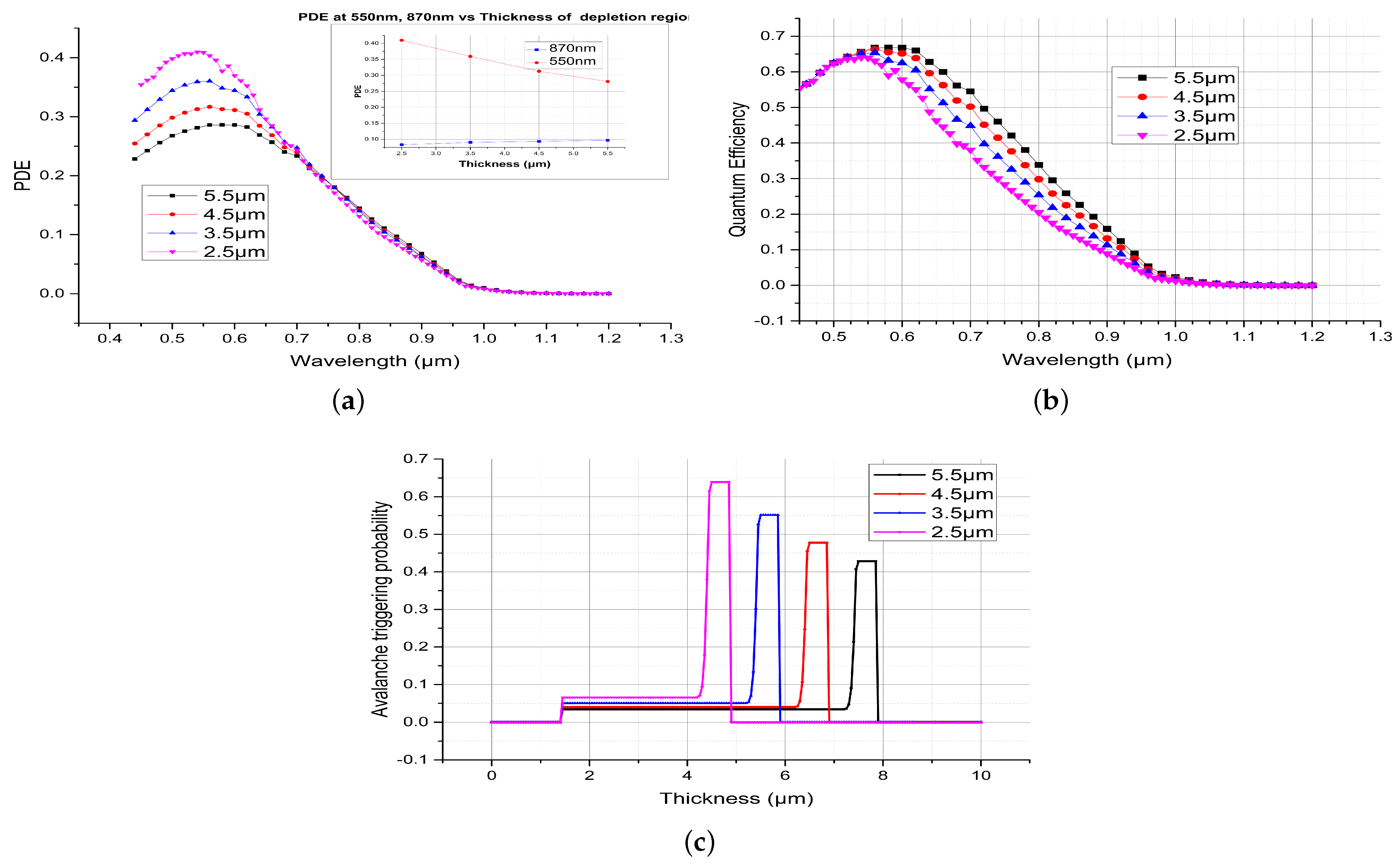
3.2. Effect of Depletion Region Thickness
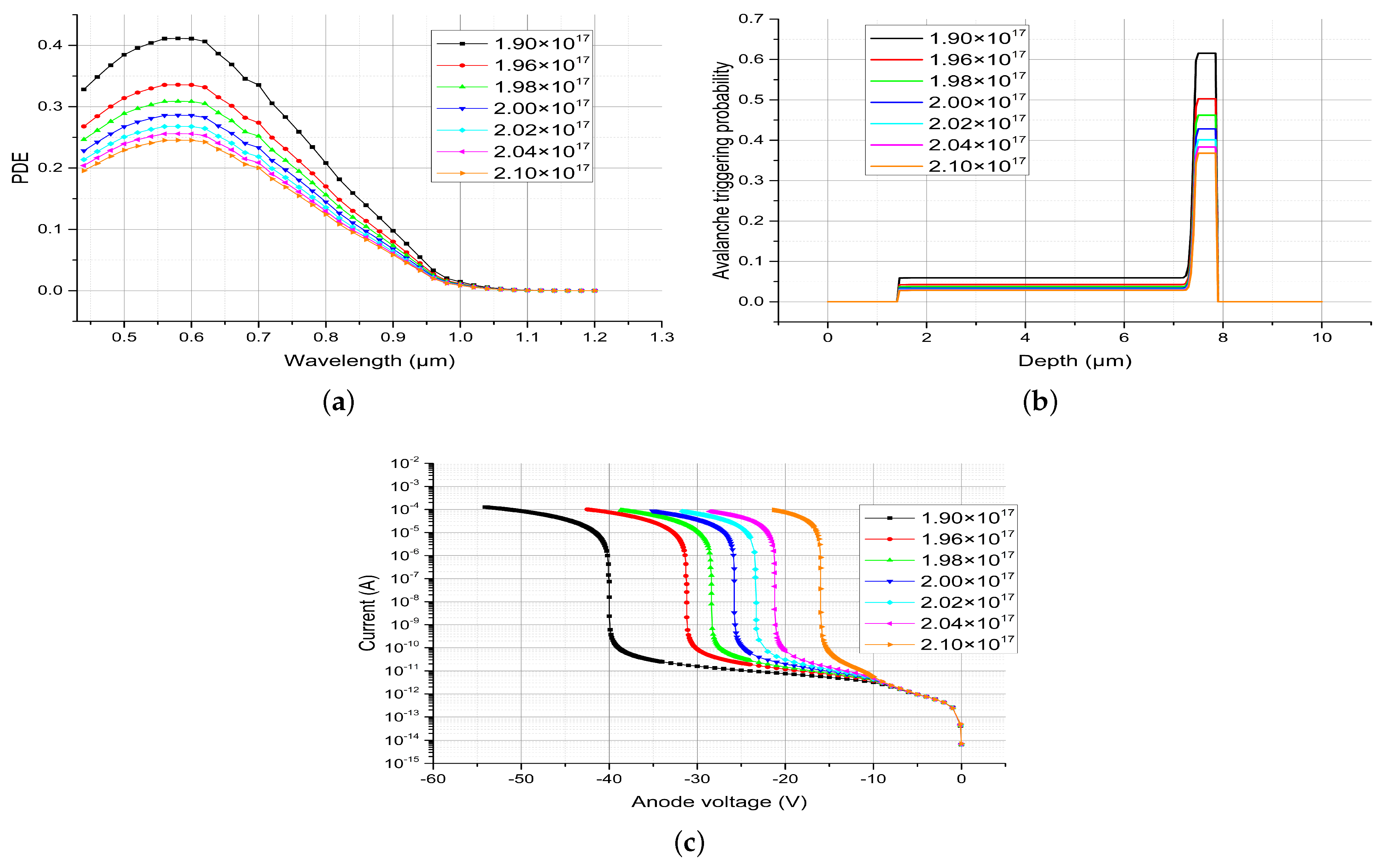
3.3. Effect of Doping Concentration of N Buried Layer
4. Conclusions
Author Contributions
Funding
Data Availability Statement
Acknowledgments
Conflicts of Interest
References
- Campbell, J. Recent Advances in Avalanche Photodiodes. J. Light. Technol. 2016, 34, 278–285. [Google Scholar] [CrossRef]
- Steindl, B.; Hofbauer, M.; Schneider-Hornstein, K.; Brandl, P.; Zimmermann, H. Single-photon avalanche photodiode based fiber optic receiver for up to 200 Mb/s. IEEE J. Sel. Top. Quantum Electron. 2017, 24, 1–8. [Google Scholar] [CrossRef]
- Gyongy, I.; Al Abbas, T.; Finlayson, N.; Johnston, N.; Calder, N.; Erdogan, A.; Dutton, N.W.; Walker, R.; Henderson, R.K. Advances in CMOS SPAD sensors for LIDAR applications. Emerg. Imaging Sens. Technol. Secur. Def. III 2018, 10799, 1079907. [Google Scholar]
- Bruschini, C.; Homulle, H.; Antolovic, I.M.; Burri, S.; Charbon, E. Single-photon avalanche diode imagersin biophotonics: Review and outlook. Light. Sci. Appl. 2019, 8, 1–28. [Google Scholar] [CrossRef] [PubMed]
- Faramarzpour, N.; Deen, M.J.; Shirani, S.; Fang, Q. Fully Integrated Single Photon Avalanche Diode Detector in Standard CMOS 0.18 μm Technology. IEEE Trans. Electron Devices 2008, 55, 760–767. [Google Scholar] [CrossRef]
- Wei, W.; Yu, Z.; Wei, Z. High-Performance Structure of Guard Ring in Avalanche Diode for Single Photon Detection. Int. J. Commun. Netw. Syst. Sci. 2017, 10, 1–6. [Google Scholar]
- Richardson, J.A.; Webster, E.; Grant, L.A.; Henderson, R.K. Scaleable Single-Photon Avalanche Diode Structures in Nanometer CMOS Technology. IEEE Trans. Electron Devices 2011, 58, 2028–2035. [Google Scholar] [CrossRef]
- Niclass, C.; Matsubara, H.; Soga, M.; Ohta, M.; Ogawa, M.; Yamashita, T. A NIR-Sensitivity-Enhanced Single-Photon Avalanche Diode in 0.18 µm CMOS. In Proceedings of the International Image Sensor Workshop, Vaals, The Netherlands, 8–11 June 2015; pp. 8–11. [Google Scholar]
- Takai, I.; Matsubara, H.; Soga, M.; Ohta, M.; Ogawa, M.; Yamashita, T. Single-Photon Avalanche Diode with Enhanced NIR-Sensitivity for Automotive LIDAR Systems. Sensors 2016, 16, 459. [Google Scholar] [CrossRef] [PubMed]
- Ping, X.; Yue, X. Improved photon detection efficiency of single photon avalanche diodes with buried layer structure. In Proceedings of the 2016 13th IEEE International Conference on Solid-State and Integrated Circuit Technology (ICSICT), Hangzhou, China, 25–28 October 2016. [Google Scholar]
- Pancheri, L.; Stoppa, D.; Betta, G.D. Characterization and Modeling of Breakdown Probability in Sub-Micrometer CMOS SPADs. IEEE J. Sel. Top. Quantum Electron. 2014, 20, 328–335. [Google Scholar] [CrossRef]
- Shao, L.; Li, T.; Chen, Y.X.; Wang, Y. Design and Optimization of 500 V Trench Anode LIGBT. J. Beijing Univ. Technol. 2012, 38, 1153–1157. [Google Scholar]


| Region | Value () | Type |
|---|---|---|
| N+ | uniformity | |
| N Well | uniformity | |
| N− | uniformity | |
| P well | uniformity | |
| N buried layer | gauss | |
| P buried layer | gauss |
Publisher’s Note: MDPI stays neutral with regard to jurisdictional claims in published maps and institutional affiliations. |
© 2021 by the authors. Licensee MDPI, Basel, Switzerland. This article is an open access article distributed under the terms and conditions of the Creative Commons Attribution (CC BY) license (https://creativecommons.org/licenses/by/4.0/).
Share and Cite
Du, Y.; Li, B.; Wang, X. Simulation Study of Silicon-Based Single-Photon Avalanche Diodes with Double Buried Layers and Deep Trench Electrodes. Crystals 2021, 11, 1176. https://doi.org/10.3390/cryst11101176
Du Y, Li B, Wang X. Simulation Study of Silicon-Based Single-Photon Avalanche Diodes with Double Buried Layers and Deep Trench Electrodes. Crystals. 2021; 11(10):1176. https://doi.org/10.3390/cryst11101176
Chicago/Turabian StyleDu, Yanyan, Bo Li, and Xu Wang. 2021. "Simulation Study of Silicon-Based Single-Photon Avalanche Diodes with Double Buried Layers and Deep Trench Electrodes" Crystals 11, no. 10: 1176. https://doi.org/10.3390/cryst11101176
APA StyleDu, Y., Li, B., & Wang, X. (2021). Simulation Study of Silicon-Based Single-Photon Avalanche Diodes with Double Buried Layers and Deep Trench Electrodes. Crystals, 11(10), 1176. https://doi.org/10.3390/cryst11101176