


Journal Description
Micromachines
Micromachines
is a peer-reviewed, open access journal on the science and technology of small structures, devices and systems, published monthly online by MDPI. The Chinese Society of Micro-Nano Technology (CSMNT) and AES Electrophoresis Society are affiliated with Micromachines and their members receive a discount on the article processing charges.
- Open Access— free for readers, with article processing charges (APC) paid by authors or their institutions.
- High Visibility: indexed within Scopus, SCIE (Web of Science), PubMed, PMC, Ei Compendex, dblp, and other databases.
- Journal Rank: JCR - Q2 (Instruments and Instrumentation) / CiteScore - Q1 (Mechanical Engineering)
- Rapid Publication: manuscripts are peer-reviewed and a first decision is provided to authors approximately 16.6 days after submission; acceptance to publication is undertaken in 2.6 days (median values for papers published in this journal in the first half of 2026).
- Recognition of Reviewers: Reviewers whose reports are timely and of high quality receive an APC discount voucher for a future publication in an MDPI journal. Become a reviewer.
- Companion journal: Micro.
- Journal Cluster of Instruments and Instrumentation: Actuators, AI Sensors, Instruments, Metrology, Micromachines and Sensors.
Impact Factor:
3.5 (2025);
5-Year Impact Factor:
3.5 (2025)
Latest Articles
Collective Motion and Programmable Self-Organization of Rotating Active Particles Manipulated by Magnetic Fields
Micromachines 2026, 17(9), 1068; https://doi.org/10.3390/mi17091068 (registering DOI) - 9 Sep 2026
Abstract
►
Show Figures
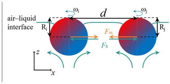
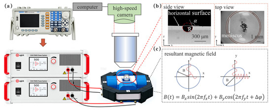
Rotating magnetic microparticles are classic active matter systems dominated by competing magnetic dipolar attraction and spin-induced hydrodynamic repulsion, whose collective behaviors under programmable magnetic field remain insufficiently characterized. This work builds a two-dimensional orthogonal Helmholtz coil experimental setup to investigate the collective motion
[...] Read more.
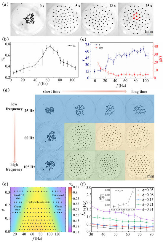
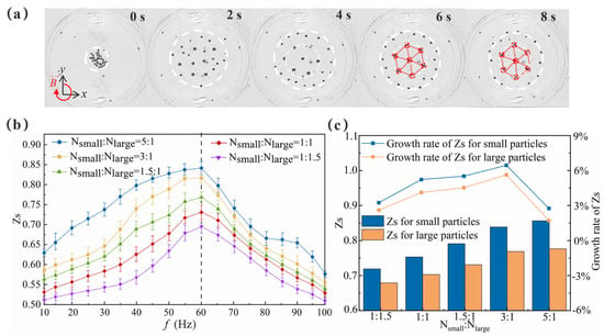
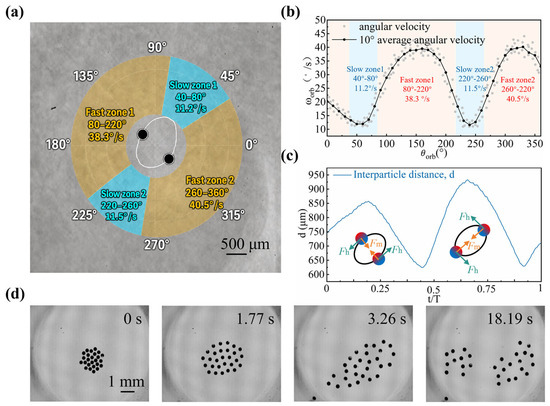
Rotating magnetic microparticles are classic active matter systems dominated by competing magnetic dipolar attraction and spin-induced hydrodynamic repulsion, whose collective behaviors under programmable magnetic field remain insufficiently characterized. This work builds a two-dimensional orthogonal Helmholtz coil experimental setup to investigate the collective motion and self-organization of magnetic microparticles. For single-component assemblies, the hexatic order parameter varies non-monotonically with driving frequency and particle area fraction; an intermediate frequency range (60–80 Hz) yields optimal hexagonally ordered structures, and a full phase diagram covering clustered, ordered and disordered states is established. Binary mixtures of 200 μm and 300 μm particles display hydrodynamic driven size segregation, with the segregation parameter peaking uniformly at 60 Hz. By applying programmable Lissajous-type magnetic fields with mismatched orthogonal frequencies, we achieve tunable elliptical particle trajectories and controlled splitting of particle clusters. This study reveals the coupling mechanism between magnetic and finite Reynolds number hydrodynamic interactions and proposes a programmable method to dynamically reconfigure active microparticle swarms.
Full article
Open AccessArticle
Nanomaterial-Based SPR Sensing Chip for Detection of Metal Ion Mixtures in Aquatic Environment
by
Jie Li, Xiaomeng Zhang, Chong Yue and Wenbin Yin
Micromachines 2026, 17(9), 1067; https://doi.org/10.3390/mi17091067 (registering DOI) - 9 Sep 2026
Abstract
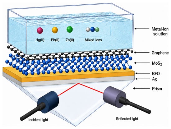
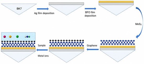
Aquatic heavy metal pollution poses substantial risks to ecological systems and human health, attributable to the toxic properties and bioaccumulative behaviors of metallic ions, including Hg[II], Zn[II], and ion mixtures. A novel SPR sensing chip based on a Ag-BiFeO3-MoS2–graphene
[...] Read more.
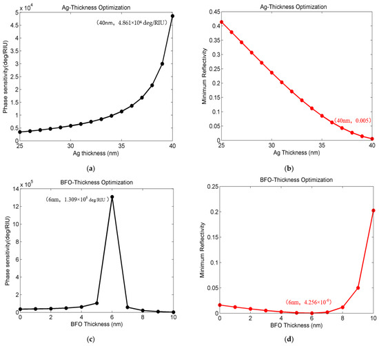
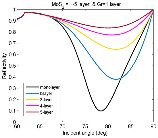
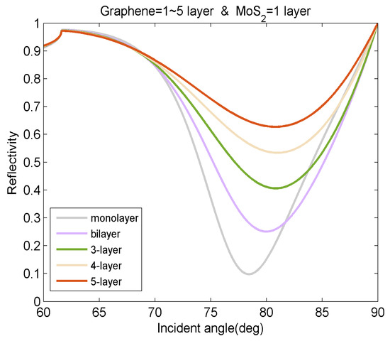
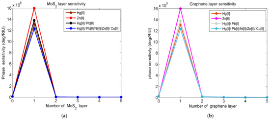
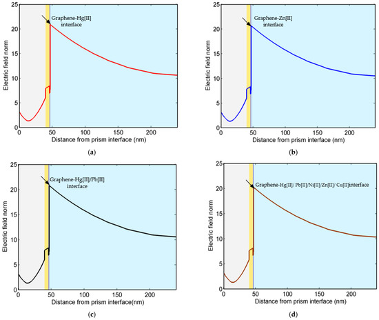
Aquatic heavy metal pollution poses substantial risks to ecological systems and human health, attributable to the toxic properties and bioaccumulative behaviors of metallic ions, including Hg[II], Zn[II], and ion mixtures. A novel SPR sensing chip based on a Ag-BiFeO3-MoS2–graphene hybrid structure is proposed and analyzed for detection of metal ion mixtures. Systematic tuning is implemented for Ag and BiFeO3 film thicknesses to boost the overall sensing capability, aiming to acquire minimized reflectance together with favorable detection sensitivity. Following this step, we investigate how different quantities of MoS2 and graphene layers affect the sensing properties of the SPR biosensor. Analytical outcomes demonstrate that configurations adopting monolayer MoS2 and graphene achieve the maximum phase sensitivity. Moreover, the optimized SPR chip architecture achieves sensing sensitivity two orders of magnitude greater than conventional sensor setups. Numerical investigations are further carried out to evaluate the sensor’s response toward various heavy metal ion species. The maximal sensitivity of 1.599 × 10⁶ deg/RIU is realized when detecting Zn[II]. Under this optimal structural setup, the spatial electric field distributions responding to variations in the refractive index of the sensing medium are also characterized. The remarkable sensitivity of the presented sensor configuration makes it a more competitive choice for deployment in further biological detection scenarios.
Full article
(This article belongs to the Special Issue Nanomaterials for Micro/Nano Devices, 3rd Edition)
►▼
Show Figures

Figure 1
Open AccessArticle
Reusable and Soft Self-Adhesive Epidermal Electrodes for Human Skin Enabled by Functional Additives
by
Sungmin Bae, Dong-Jin Lee, Chuljin Hwang and Dae Yu Kim
Micromachines 2026, 17(9), 1066; https://doi.org/10.3390/mi17091066 - 8 Sep 2026
Abstract
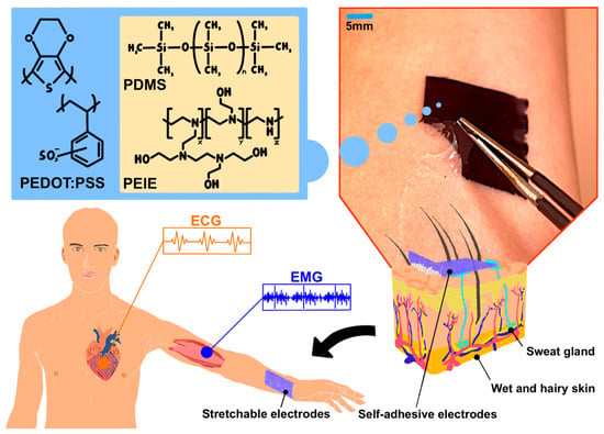
Wearable electronics, particularly dry epidermal electrodes, provide human-connected interfaces for recording biopotential signals. However, their practical utility is often hindered by their limited operational longevity and the resulting environmental burden of electronic waste, as most conventional electrodes are discarded after a single use
[...] Read more.
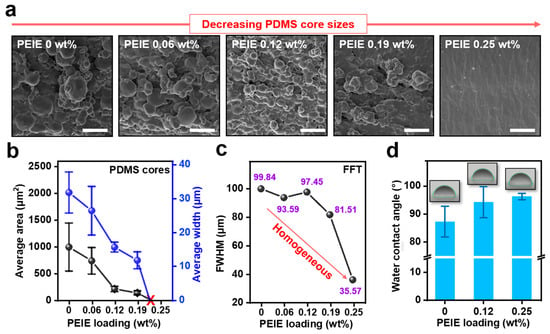
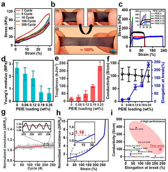
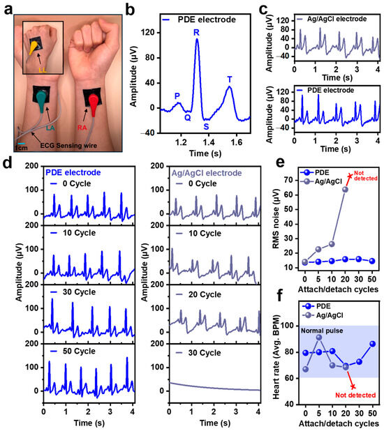
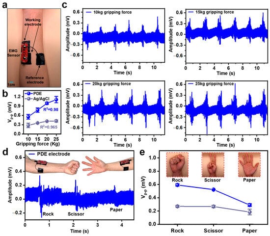
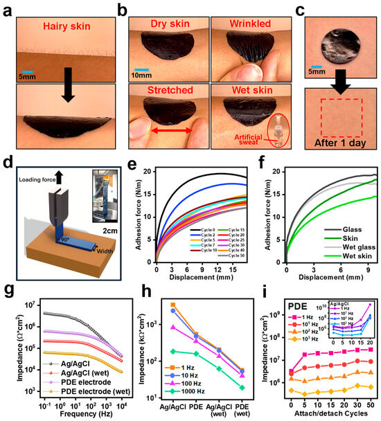
Wearable electronics, particularly dry epidermal electrodes, provide human-connected interfaces for recording biopotential signals. However, their practical utility is often hindered by their limited operational longevity and the resulting environmental burden of electronic waste, as most conventional electrodes are discarded after a single use because of performance degradation. Herein, a reusable, soft, and conductive epidermal electrode is reported, fabricated through the precise incorporation of functional additives. By intentionally modulating the polymer chain architecture, a homogeneous composite is developed that exhibits exceptional flexibility, high conductivity (~100 S/cm), softness (~649 kPa), and stretchability (~234%). This molecular-level design promotes strong intermolecular interactions at the skin–electrode interface, facilitating persistent adhesion and conformability to challenging surfaces, including wet, wrinkled, and stretched skin. These properties enable reliable electrocardiography acquisition through 50 repeated attachment and detachment cycles, over which a commercial Ag/AgCl gel electrode became unmeasurable after 20. The applicability of the electrode to human–machine interfaces is further demonstrated by capturing clear electromyography signals of muscle activity during a rock–paper–scissors game. This low-modulus electrode platform offers a route towards repeated-use wearable healthcare systems and soft-robotics applications, with the potential to reduce the waste associated with single-use electrodes.
Full article
(This article belongs to the Special Issue Flexible and Wearable Sensors, 4th Edition)
►▼
Show Figures

Figure 1
Open AccessReview
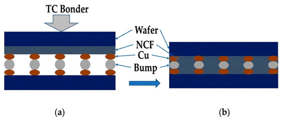
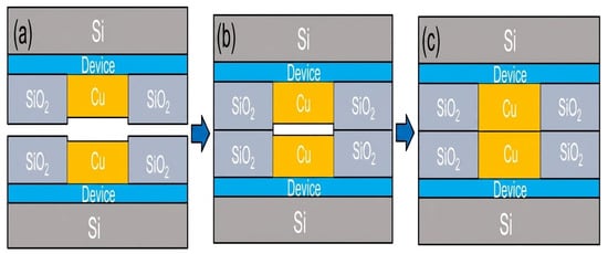
Thermal Management and Reliability Engineering of Advanced HBM Packages: Materials, Interfaces, and Integrated Design Strategies
by
Hye Rin Do, Jun Ha Wee, Hwa Rim Lee, Young Chae Lee, Yunna Song and Sung Gyu Pyo
Micromachines 2026, 17(9), 1065; https://doi.org/10.3390/mi17091065 - 8 Sep 2026
Abstract
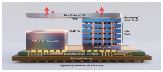
Advances in artificial intelligence, high-performance computing, and generative AI technologies have driven a rapid increase in the memory bandwidth and data throughput required of semiconductor systems, establishing High Bandwidth Memory (HBM)—which vertically stacks multiple DRAM dies—as a key enabling memory technology. However, increasing
[...] Read more.
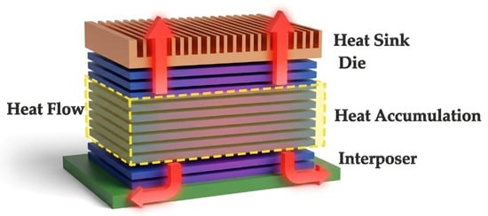
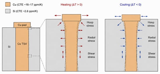
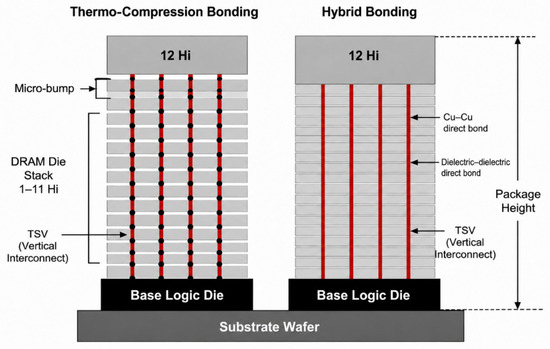
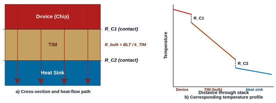
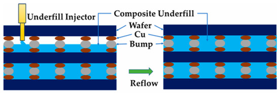
Advances in artificial intelligence, high-performance computing, and generative AI technologies have driven a rapid increase in the memory bandwidth and data throughput required of semiconductor systems, establishing High Bandwidth Memory (HBM)—which vertically stacks multiple DRAM dies—as a key enabling memory technology. However, increasing the stack count and shrinking the interconnect pitch in HBM not only intensify vertical heat accumulation and hotspot formation but also give rise to complex reliability issues, including thermo-mechanical stress arising from coefficient-of-thermal-expansion (CTE) mismatch, package warpage, interfacial delamination, Cu protrusion, void formation, and joint degradation. This review analyzes the heat-generation and heat-transfer mechanisms of HBM packages and examines package-level thermal management strategies based on thermal interface materials, underfill, non-conductive film, epoxy molding compound, heat spreaders, and high-thermal-conductivity composites. It further summarizes the current crowding, electromigration, Cu–dielectric interfacial defects, and thermo-mechanical failure mechanisms that arise at fine-pitch interconnects and hybrid-bonding interfaces, together with the material and process design strategies developed to mitigate them. In addition, structure-based thermal management technologies—thermal TSVs, embedded cooling, and hybrid bonding—are compared. This review emphasizes that the thermal bottlenecks and reliability degradation of HBM are interconnected through interfacial thermal resistance, interfacial adhesion, residual stress, and interfacial defects, and proposes that next-generation, highly stacked HBM requires a multi-scale thermal-reliability co-design that integrally controls the heat-, stress-, and current-transfer pathways across the entire package and interconnect domain, rather than relying on the improvement of individual material properties alone.
Full article
(This article belongs to the Special Issue Semiconductor Materials and Processing Technology)
►▼
Show Figures

Figure 1
Open AccessArticle
Error State Kalman Filter for Integrated Attitude Estimation Based on Data Fusion of MIMU Inertial Array and Magnetometer
by
Liang Xue, Jixiang Lu, Guangbin Cai, Bo Yang and Xinguo Wang
Micromachines 2026, 17(9), 1064; https://doi.org/10.3390/mi17091064 - 8 Sep 2026
Abstract
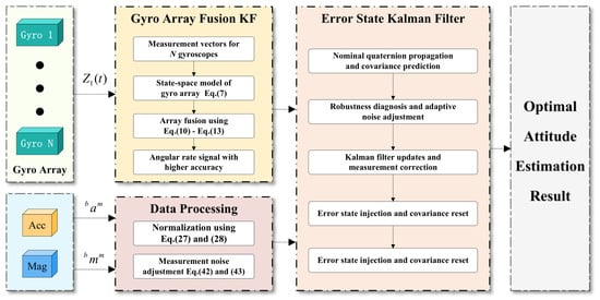
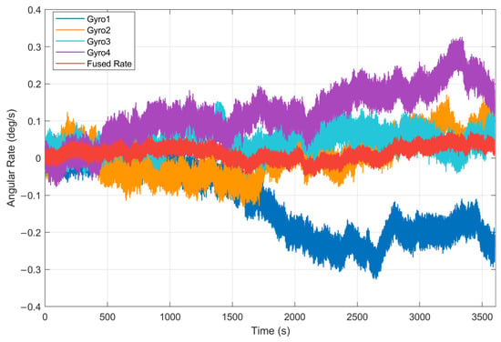
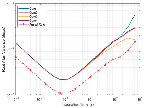
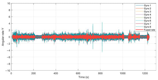
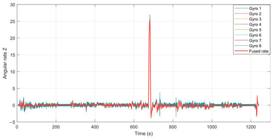
Attitude estimation has increasingly relied on MEMS inertial measurement units (IMUs) owing to the low cost and miniature size, but the inherent high random noise and error accumulation limit long-term measurement accuracy. This article proposes an integrated attitude estimation algorithm based on data
[...] Read more.
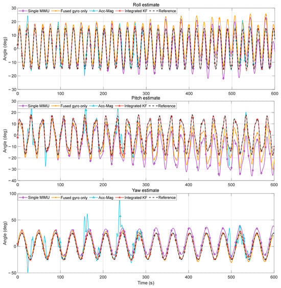
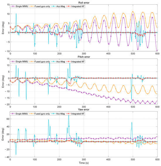
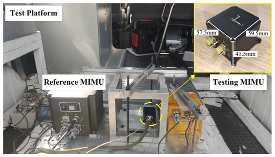
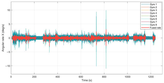
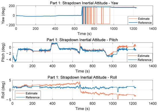
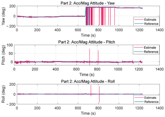
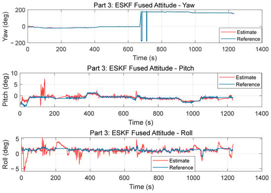
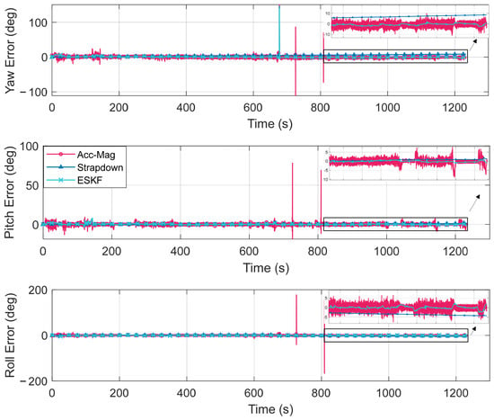
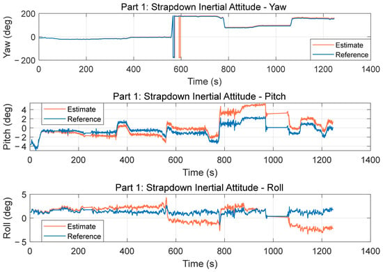
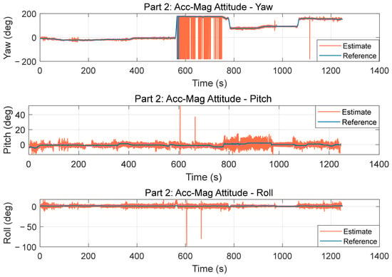
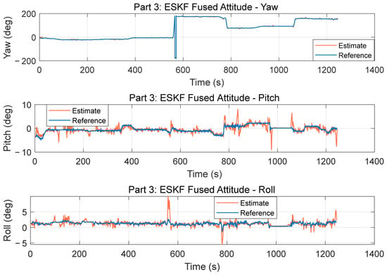
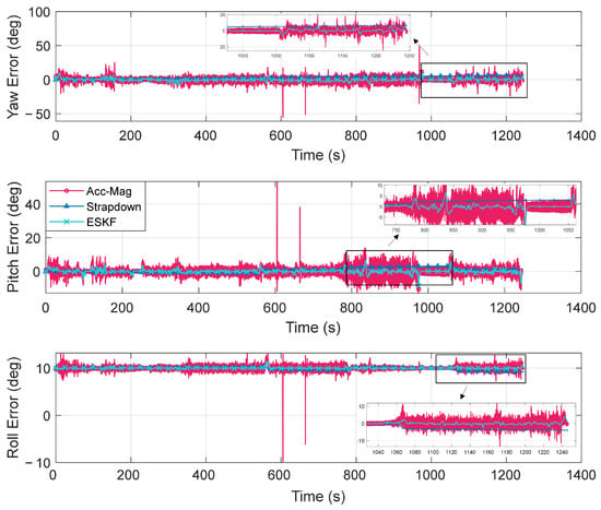
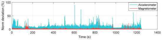
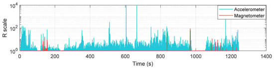
Attitude estimation has increasingly relied on MEMS inertial measurement units (IMUs) owing to the low cost and miniature size, but the inherent high random noise and error accumulation limit long-term measurement accuracy. This article proposes an integrated attitude estimation algorithm based on data fusion from a MIMU inertial array and magnetometer to address this challenge. First, a redundant inertial array is constructed using homogeneous gyroscopes, and a Kalman filter (KF) is designed to fuse output signals from multiple gyroscopes to estimate true angular rate. Second, an integrated error state Kalman filter (ESKF) for the MIMU/magnetometer system is developed. Using the attitude quaternion calculated by the strapdown inertial solution as the nominal state and combining it with measurements from the accelerometer and magnetometer as observations, the attitude error is estimated and corrected. Both simulations and field experiments were conducted to validate the effectiveness of the proposed algorithm. The experimental results show that the ESKF algorithm performs best in estimation accuracy and addresses the issue of error accumulation and fluctuation. In particular, the Root Mean Square Error (RMSE) of the ESKF algorithm was significantly reduced, with the roll angle reduced by 55.34%, the pitch angle by 30.25%, and the yaw angle by 55.71%.
Full article
(This article belongs to the Special Issue MEMS Inertial Device, 3rd Edition)
►▼
Show Figures

Figure 1
Open AccessArticle
Phase Compensator Combined Feedback Control to Mitigate Dynamic Hysteresis in Piezoelectric Actuators
by
Zhen Wang, Zekun Li, Hanqing Liu, Guanglu Hao, Bo Li and Kairui Cao
Micromachines 2026, 17(9), 1063; https://doi.org/10.3390/mi17091063 - 8 Sep 2026
Abstract
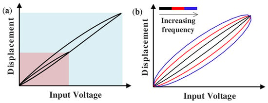
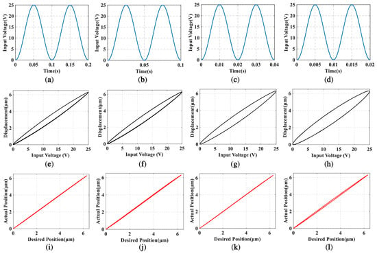
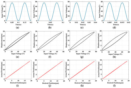
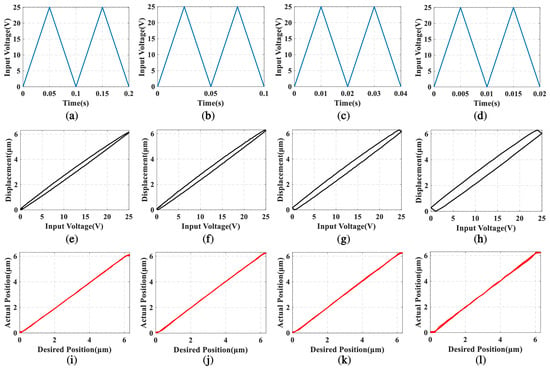
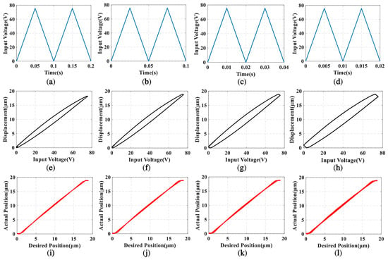
The inherent dynamic hysteresis nonlinearity of piezoelectric actuators severely degrades the control accuracy of micropositioning systems. This paper proposes a composite control method based on a phase compensator and polynomial correction. Unlike conventional approaches that rely on hysteresis modeling and inversion, the proposed
[...] Read more.
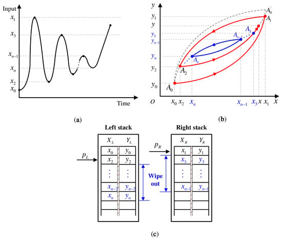
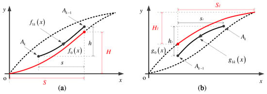
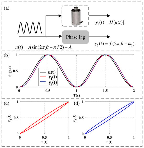
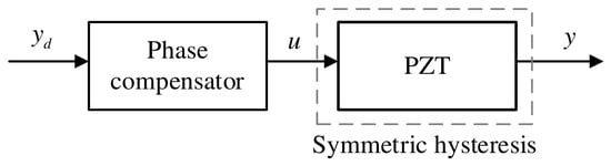
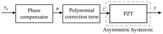
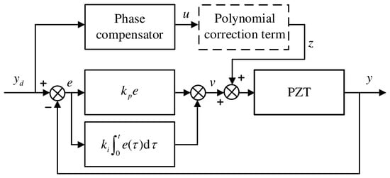
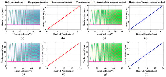
The inherent dynamic hysteresis nonlinearity of piezoelectric actuators severely degrades the control accuracy of micropositioning systems. This paper proposes a composite control method based on a phase compensator and polynomial correction. Unlike conventional approaches that rely on hysteresis modeling and inversion, the proposed method equivalently treats the symmetric hysteresis of piezoelectric actuators as a phase-lag property of the system and employs a phase compensator to achieve feedforward compensation. For asymmetric hysteresis, a polynomial is cascaded with the phase compensator to correct the amplitude discrepancy between ascending and descending branches, effectively overcoming the inability of the phase compensator alone to accommodate asymmetric nonlinearity. This strategy circumvents the cumbersome procedures of precise hysteresis modeling and parameter identification, offering a simple structure, few parameters to be identified, and convenient engineering implementation within the investigated operating range. To further enhance disturbance-rejection capability and steady-state positioning accuracy, the phase–polynomial feedforward compensator is combined with PI feedback control, establishing a composite feedforward–feedback architecture for high-performance piezoelectric actuator control. Feedforward compensation and composite control experiments validate the effectiveness of the proposed method.
Full article
(This article belongs to the Section E:Engineering and Technology)
►▼
Show Figures

Figure 1
Open AccessArticle
A High-Sensitivity MEMS Pressure Sensor with a Narrow Cross-Beam Membrane–Short Beam Structure
by
Tao Wang, Zibang Xiao, Peicang Chen, Meng Nie, Zhen Yan, Shijie Deng, Jing Chen, Xiaolin Wang and Jingquan Liu
Micromachines 2026, 17(9), 1062; https://doi.org/10.3390/mi17091062 - 8 Sep 2026
Abstract
To address the difficulty of balancing sensitivity and nonlinearity in MEMS piezoresistive pressure sensors, this study proposes an MEMS piezoresistive pressure sensor with a narrow cross-beam membrane–short beam structure. The structure introduces a tapered design at the ends of a conventional cross beam
[...] Read more.
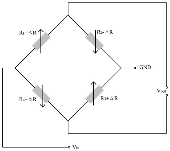
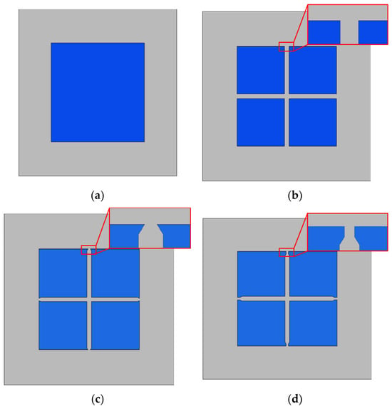
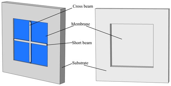
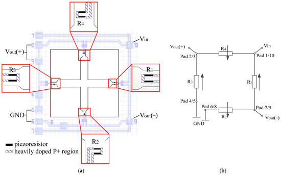
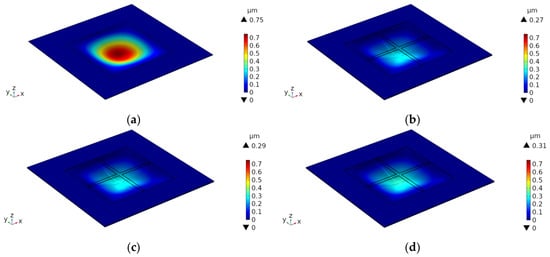
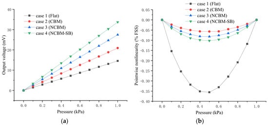
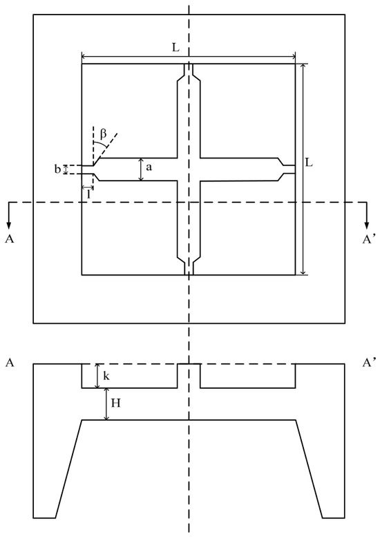
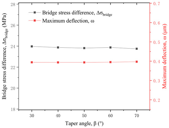
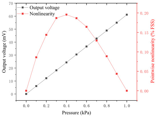
To address the difficulty of balancing sensitivity and nonlinearity in MEMS piezoresistive pressure sensors, this study proposes an MEMS piezoresistive pressure sensor with a narrow cross-beam membrane–short beam structure. The structure introduces a tapered design at the ends of a conventional cross beam and incorporates short beams to enhance stress concentration in the sensitive regions, thereby improving output sensitivity while maintaining low nonlinearity. Finite-element analysis was performed to evaluate the stress distribution and deflection characteristics and to compare the proposed structure with conventional cross-beam and other diaphragm structures. Under identical overall dimensions, the proposed structure improves sensitivity by 61% relative to the conventional cross beam. Based on the finite-element results, multivariate fitting models for surface stress and deflection were established, and nonlinear optimization was used to determine the constrained optimal geometrical parameters within the validated design domain. Simulation results indicate that, over a pressure range of 0–1 kPa, the proposed sensor achieves a sensitivity of 12.23 mV/V/kPa and a maximum nonlinearity of 0.196% FSS, demonstrating favorable performance for micropressure detection.
Full article
(This article belongs to the Special Issue MEMS and NEMS Sensors: Innovations, Applications, and Future Directions in Micro/Nano Technologies)
►▼
Show Figures

Figure 1
Open AccessArticle
Design and Implementation of a Quartz Cilia MEMS Vector Hydrophone
by
Ziming Ren, Shijie Yang, Rushan Xie, Zhonggang Zhang, Libo Gao and Chenyang Xue
Micromachines 2026, 17(9), 1061; https://doi.org/10.3390/mi17091061 - 6 Sep 2026
Abstract
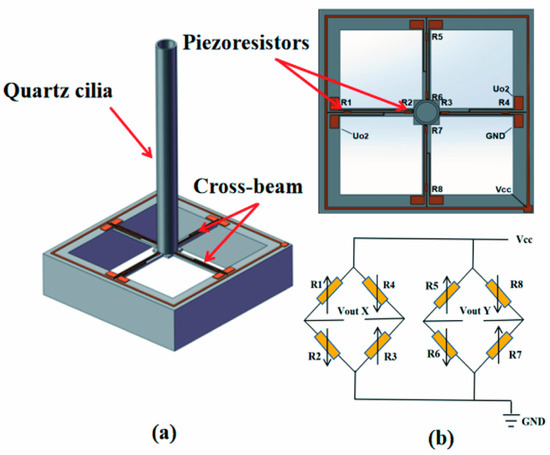
The cilium avoids energy loss due to bending deformation during vibration, thereby efficiently transmitting the acoustic driving force to the cross-beam. Meanwhile, a hollow cylindrical structure is adopted instead of the traditional solid one. While maintaining the same external geometry, this hollow design
[...] Read more.
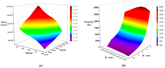
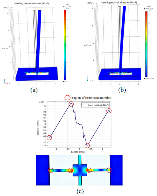
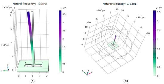
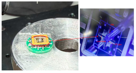
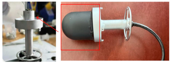
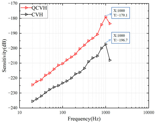
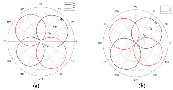
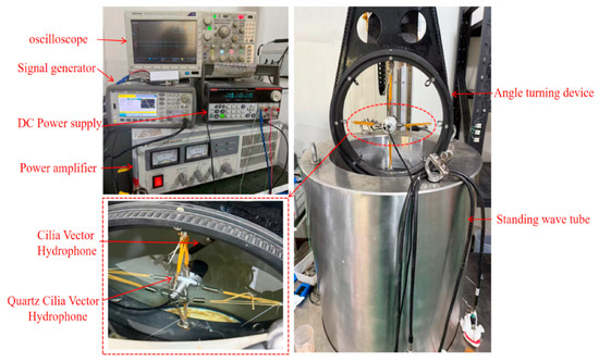
The cilium avoids energy loss due to bending deformation during vibration, thereby efficiently transmitting the acoustic driving force to the cross-beam. Meanwhile, a hollow cylindrical structure is adopted instead of the traditional solid one. While maintaining the same external geometry, this hollow design not only increases the effective acoustic area to enhance the acoustic driving force but also reduces the added mass of the cilium. This material–structure synergistic optimization improves the acoustic-to-mechanical transfer efficiency of the cilium in low-frequency acoustic fields, thus enhancing the device’s acoustic sensitivity in the low-frequency range. Parametric simulations are conducted using the COMSOL Multiphysics 6.3 platform to systematically optimize key geometric parameters such as the outer radius and height of the quartz cilium, and the optimal dimensions are determined. The sensitivity and directivity of the prototype are measured in the 20–1000 Hz frequency range using the standard hydrophone comparison method. Experimental results show that the quartz cilium vector hydrophone achieves a sensitivity of –179.1 dB (1 kHz, 0 dB = 1 V/μPa) at 1000 Hz. The frequency response curve exhibits good flatness in the low-frequency range and agrees well with the theoretical 6 dB per octave increase characteristic of pressure gradient sensors. Directivity tests reveal a typical figure-8 pattern at both 315 Hz and 630 Hz, with null depths exceeding 30 dB, demonstrating excellent vector detection capability. This study provides an effective approach for improving the low-frequency sensitivity of MEMS (Micro-Electromechanical System) vector hydrophones, and the designed device meets the requirements for underwater target detection with promising prospects for engineering applications.
Full article
(This article belongs to the Special Issue Micro/Nano Technologies for Ocean Sensing and Instrumentation)
►▼
Show Figures

Figure 1
Open AccessArticle
Topology-Free EM Modeling and Analysis of Pixelated Microstrip Low-Pass Filters Under Comparable Footprint
by
Jorge Davalos-Guzman, Jose L. Chavez-Hurtado and Lina M. Aguilar-Lobo
Micromachines 2026, 17(9), 1060; https://doi.org/10.3390/mi17091060 - 6 Sep 2026
Abstract
Pixelated electromagnetic representations enable topology-free numerical exploration of microwave layouts without enforcing a predefined circuit template. This work presents a simulation-based electromagnetic modeling and analysis framework for pixelated microstrip low-pass filters within a physical footprint comparable to that of a classical stepped-impedance reference.
[...] Read more.
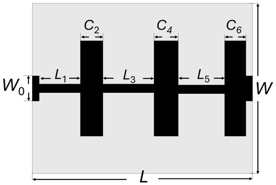
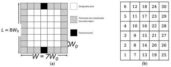
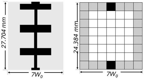
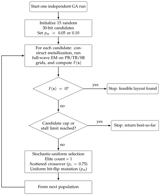
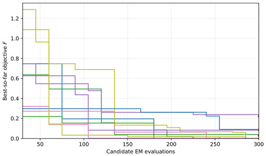
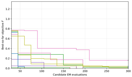
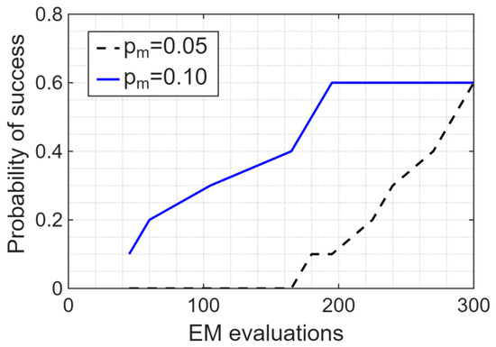
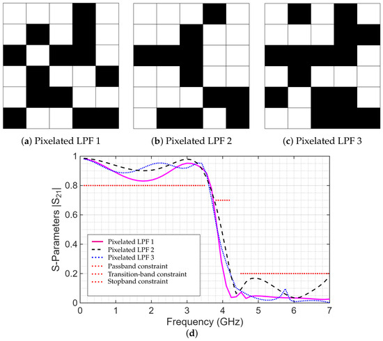
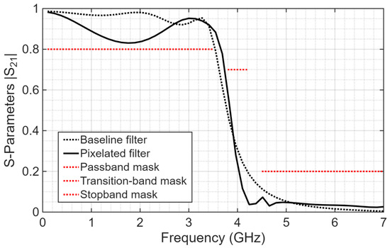
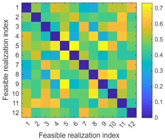
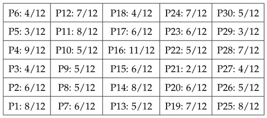
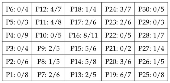
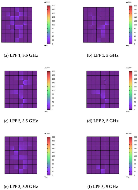
Pixelated electromagnetic representations enable topology-free numerical exploration of microwave layouts without enforcing a predefined circuit template. This work presents a simulation-based electromagnetic modeling and analysis framework for pixelated microstrip low-pass filters within a physical footprint comparable to that of a classical stepped-impedance reference. A binary metallization encoding is embedded in a fixed microstrip domain and explored through full-wave electromagnetic optimization under consistent material, excitation, and specification conditions. The objective is not extreme miniaturization or hardware prototyping, but to assess whether topology-free pixelated layouts can produce useful low-pass responses within the same general physical scale and to analyze the structural properties of the resulting feasible layouts. Across 20 independent optimization runs, 12 specification-compliant and geometrically unique metallization layouts were identified. Aggregate analysis of 360 single-pixel perturbations reveals topology-dependent sensitivity, while finite-width regularization of ideal corner contacts preserves modeled specification compliance after refined-mesh verification, with the suitable bridge width depending on the topology. The scope is deliberately limited to full-wave EM modeling and numerical analysis; experimental fabrication and measurement are left as a subsequent validation stage. These findings support topology-free pixelated EM modeling and analysis as a route for investigating non-obvious low-pass filter layouts under comparable footprint constraints.
Full article
(This article belongs to the Special Issue Recent Advances in Microwave, Photonic, and Optoelectronic Devices)
►▼
Show Figures

Figure 1
Open AccessArticle
Reliability-Oriented Multi-Class Fault-Injection Acceleration for Digital Integrated Circuits via Heterogeneous Spatio-Temporal Graph Learning
by
Jiaqi Lu, Changqing Xu, Huixin Peng, Guoxing Zhang, Liang Wang, Xinfang Liao, Yi Liu and Yintang Yang
Micromachines 2026, 17(9), 1059; https://doi.org/10.3390/mi17091059 - 4 Sep 2026
Abstract
The pre-silicon reliability analysis of digital integrated circuits relies on fault-injection campaigns to characterize how single-event upsets propagate into distinct system-level outcomes. Exhaustive gate-level injection is expensive, whereas most learning-based accelerators collapse failure manifestations into a single binary label, thereby providing limited support
[...] Read more.
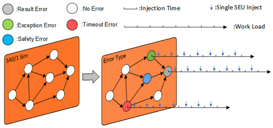
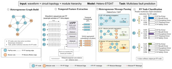
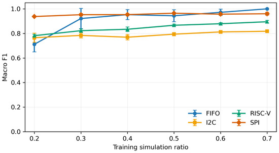
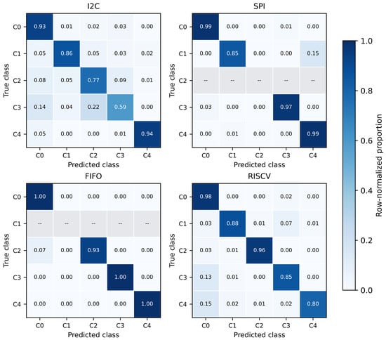
The pre-silicon reliability analysis of digital integrated circuits relies on fault-injection campaigns to characterize how single-event upsets propagate into distinct system-level outcomes. Exhaustive gate-level injection is expensive, whereas most learning-based accelerators collapse failure manifestations into a single binary label, thereby providing limited support for reliability diagnosis and follow-up analysis. We present a reliability-oriented reduced-campaign framework that predicts the monitor-defined outcome type of flip-flop (FF)-level cases omitted from a fixed circuit/workload campaign. For each circuit, Cadence Xcelium first performs SA0/SA1 screening and retains an FF when at least one stuck-at polarity produces a monitored failure. Within the resulting transient campaign, FeatureCoverage selects FF–time cases using structural attributes and fault-free activity statistics without reading their transient-fault outcomes. HSTGNN then combines a 60-cycle FF logic-value window from the same fault-free waveform, netlist-derived FF–FF topology and gate-path attributes, and module hierarchy to predict five outcomes: C0 No Error, C1 Result Error, C2 Exception Error, C3 Timeout Error, and C4 Safety Error. On the I2C, SPI, FIFO, and RISC-V benchmarks, HSTGNN achieves an 81.2–99.0% macro F1 on more than 38,000 held-out FF–time cases under a 70% labeled fault-injection budget comprising 60% training and 10% validation cases. FeatureCoverage also yields the highest macro F1 across all four label-free split strategies in every evaluated circuit. The proposed framework predicts the remaining 30% of cases while preserving reliability-relevant outcome semantics that binary acceleration discards. The evidence is limited to within-campaign prediction and supports, rather than replaces, quantitative reliability and diagnostic-coverage analysis.
Full article
(This article belongs to the Special Issue High-Reliability Semiconductor Devices and Integrated Circuits, 4th Edition)
►▼
Show Figures

Figure 1
Open AccessArticle
Investigation on FAB Morphology Evolution and Pd Redistribution Behavior in Palladium-Coated Copper Wires During Electronic Flame-Off (EFO) Process
by
Junling Fan, Haoyang Wang, Yongzhen Sun, Jun Cao and Weilong Liu
Micromachines 2026, 17(9), 1058; https://doi.org/10.3390/mi17091058 - 4 Sep 2026
Abstract
►▼
Show Figures
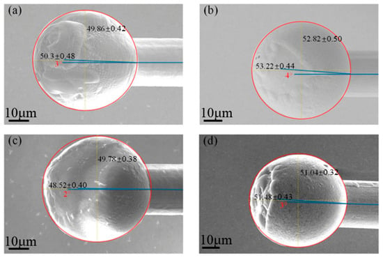
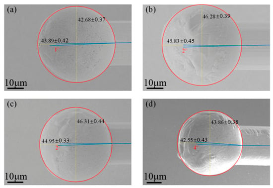
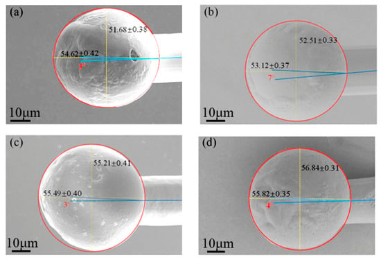
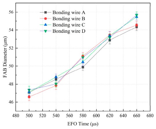
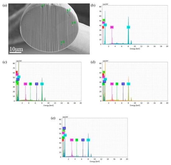
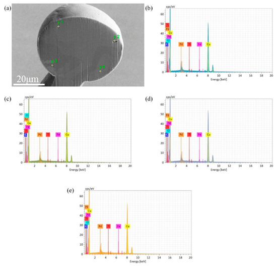
Compared with bare copper wire, palladium-coated copper (PCC) wire is widely used in microelectronic packaging due to its improved oxidation resistance and enhanced reliability. However, the formation mechanism of free air balls (FABs) and the redistribution behavior of Pd during the electronic flame-off
[...] Read more.
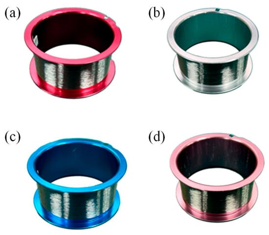
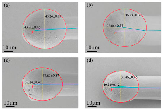
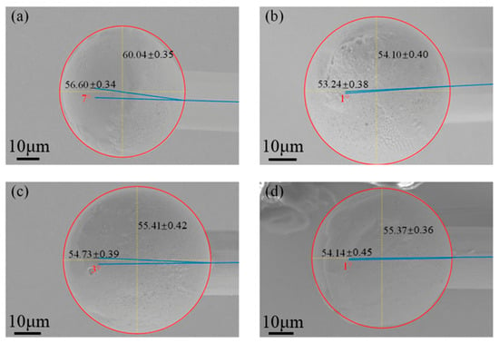
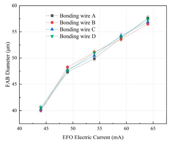
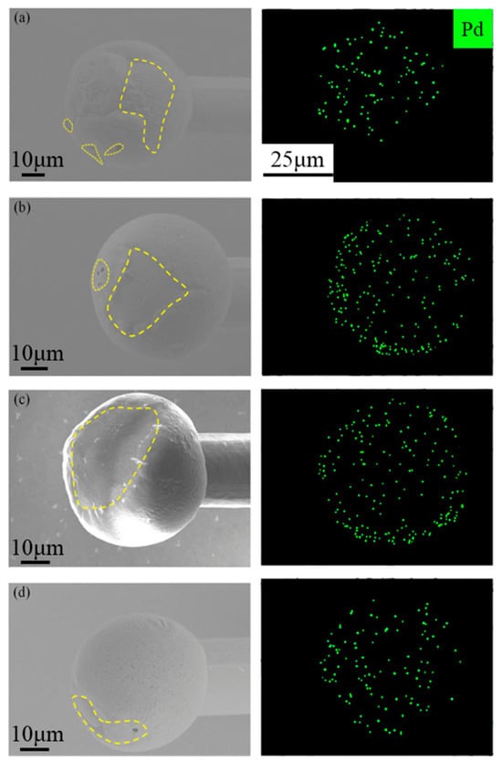
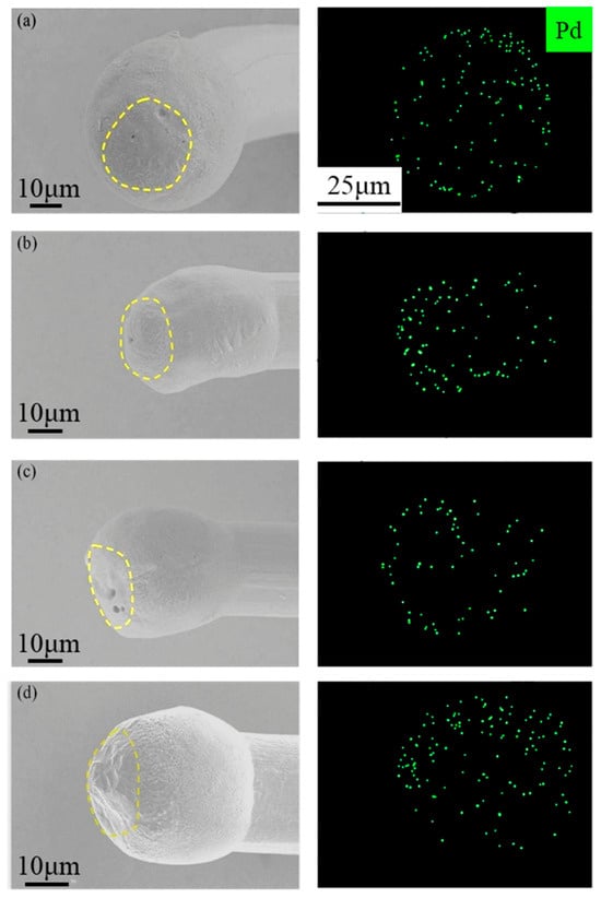
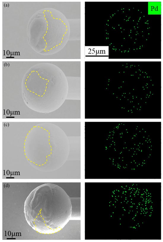
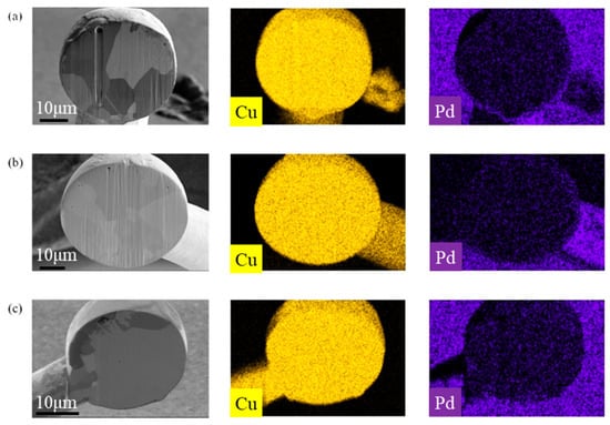
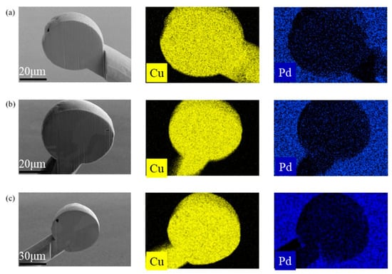
Compared with bare copper wire, palladium-coated copper (PCC) wire is widely used in microelectronic packaging due to its improved oxidation resistance and enhanced reliability. However, the formation mechanism of free air balls (FABs) and the redistribution behavior of Pd during the electronic flame-off (EFO) process, particularly under different Pd coating thicknesses and processing conditions, have not yet been fully understood. In this work, four types of 1 mil PCC wires with Pd coating thicknesses of 60, 80, 100, and 120 nm were systematically investigated to study the influence of EFO parameters on FAB morphology and Pd redistribution behavior. SEM, FIB, and EDS analyses were employed to provide experimental insights into the coupled relationship between transient thermal input, internal pore distribution and elemental segregation evolution, and Pd redistribution behavior. The results show that the preferred FAB morphology is obtained at 54 mA and 580 μs, with a diameter-to-wire ratio of approximately 2. With increasing Pd coating thickness, the exposed copper area on the FAB surface decreases from 13% to 6%, while the Pd-deficient region gradually shifts toward the bottom of the FAB. This study provides experimental insights into the Pd redistribution behavior during FAB formation under different EFO conditions, which may contribute to the optimization of Pd-coated Cu bonding wires.
Full article

Figure 1
Open AccessEditorial
Editorial for the Special Issue on Advances in Digital Manufacturing and Nano Fabrication
by
Jian Cheng, Jianguo Zhang and Qi Liu
Micromachines 2026, 17(9), 1057; https://doi.org/10.3390/mi17091057 - 4 Sep 2026
Abstract
In recent years, digital manufacturing, high-energy-beam processing, and nano- and micro-scale fabrication have developed rapidly, extending the capabilities of modern engineering and broadening their practical application [...]
Full article
(This article belongs to the Special Issue Advances in Digital Manufacturing and Nano Fabrication)
Open AccessArticle
Micro-Power Harvesting from Electromagnetic Interferences in Power Systems
by
Moreno d’Ambrosio, Gabriele Marasca, Massimo Calvo, Aldo Romani, Carmelo Corsaro and Salvatore Patané
Micromachines 2026, 17(9), 1056; https://doi.org/10.3390/mi17091056 - 3 Sep 2026
Abstract
The increasing demand for real-time monitoring systems has accelerated the adoption of distributed sensors operating in the ultra-low-power regime. However, in retrofittable and hard-to-access applications, providing a continuous external power supply is challenging, while batteries are limited by their lifetime and maintenance requirements.
[...] Read more.
The increasing demand for real-time monitoring systems has accelerated the adoption of distributed sensors operating in the ultra-low-power regime. However, in retrofittable and hard-to-access applications, providing a continuous external power supply is challenging, while batteries are limited by their lifetime and maintenance requirements. Energy harvesting represents a promising approach to enable autonomous sensor operation by exploiting ambient energy sources, including photovoltaic, thermal, mechanical, and electromagnetic sources. In this work, different circuit topologies for near-field electromagnetic energy harvesting are investigated through simulation and experimental validation. The proposed approach exploits the electromagnetic interference generated by shielded commercial power electronics, such as drivers and power supplies, as an available energy source. The results demonstrate the capability of compact and easily deployable circuits to capture and convert near-field electromagnetic energy into usable electrical power. The proposed methodology provides a flexible solution for powering low-power monitoring systems and can be adapted to different environments by tailoring the harvesting circuit parameters to the available electromagnetic source.
Full article
(This article belongs to the Special Issue MEMS and NEMS Sensors: Innovations, Applications, and Future Directions in Micro/Nano Technologies, 2nd Edition)
Open AccessArticle
Three-Dimensional Helical Antenna Array with Circular Polarization
by
Hui Peng, Kecheng Ye, Wei Nie and Yuxiang Li
Micromachines 2026, 17(9), 1055; https://doi.org/10.3390/mi17091055 - 3 Sep 2026
Abstract
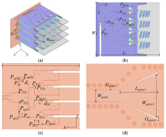
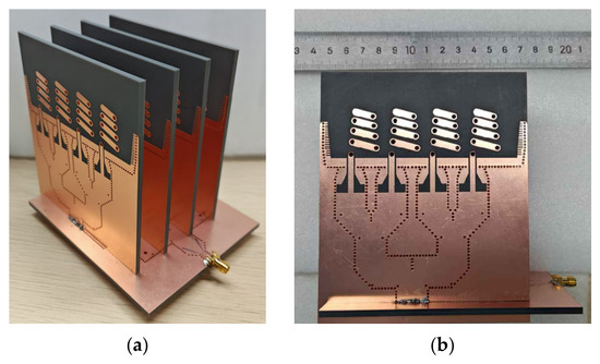
In this paper, a 4 × 4 planar helical antenna (PHA) array fed by a three-dimensional substrate integrated waveguide (SIW) power splitter is presented. The 4 × 4 array is composed of four 1 × 4 PHA subarrays, and each subarray is fed
[...] Read more.
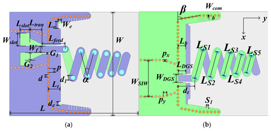
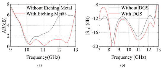
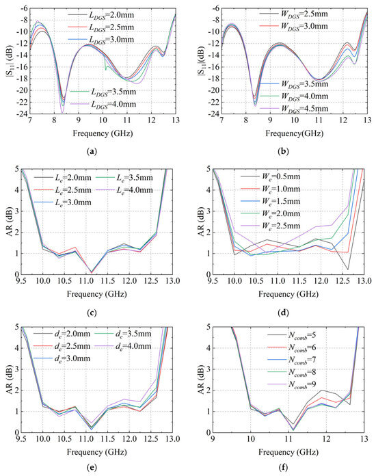
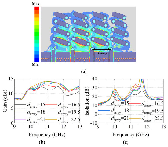
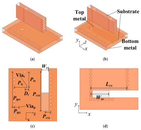
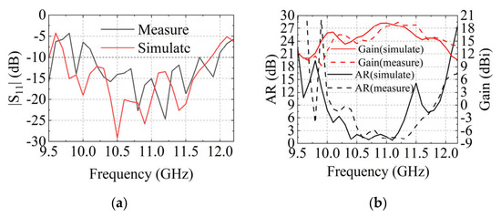
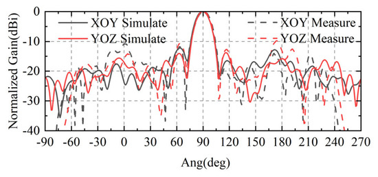
In this paper, a 4 × 4 planar helical antenna (PHA) array fed by a three-dimensional substrate integrated waveguide (SIW) power splitter is presented. The 4 × 4 array is composed of four 1 × 4 PHA subarrays, and each subarray is fed by the SIW power splitter. Since the helical antenna is end-fire, it could not be integrated into a 4 × 4 array in a 2-D plane. In order to realize a 4 × 4 array, a SIW twist vertical transition structure is designed to connect the subarray with the SIW power splitter. Finally, the proposed 4 × 4 helical antenna array is implemented and fabricated for measurement. The center frequency of the PHA is 11 GHz, the impedance bandwidth (IBW) is 10.16–11.99 GHz (16.64%), and the axial ratio bandwidth (ARBW) is 10.53–11.47 GHz with the peak gain of 18.44 dBi. The simulation and measurement results match each other well; therefore, the effectiveness of the proposed design is verified.
Full article
(This article belongs to the Special Issue Novel RF Nano- and Microsystems)
►▼
Show Figures

Figure 1
Open AccessArticle
Mechanisms of Degradation and Damage in GaAs PHEMT Low-Noise Amplifier Under Ultra-Short Microwave Pulses
by
Tongxin Guan, Liang Cheng, Zhiyuan Zhang, Yingjian Cao, Yu Wang and Guo Liu
Micromachines 2026, 17(9), 1054; https://doi.org/10.3390/mi17091054 - 3 Sep 2026
Abstract
Ultra-short microwave pulses with durations of 1 ns or less can go through a PIN limiter with low attenuation before the limiter responds and can therefore be directly injected into the subsequent low-noise amplifier (LNA). Based on this consideration, this paper reports the
[...] Read more.
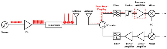
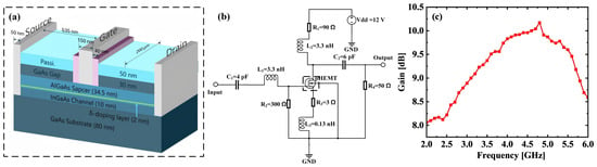
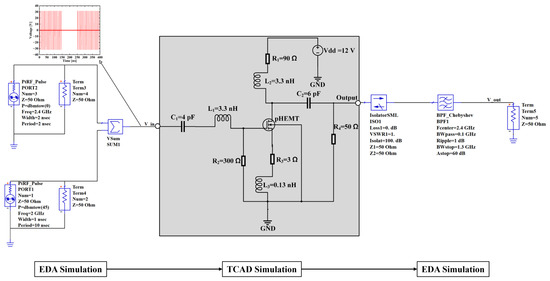
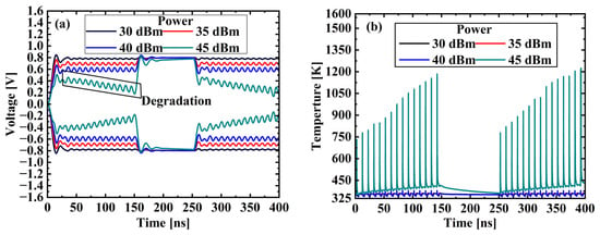
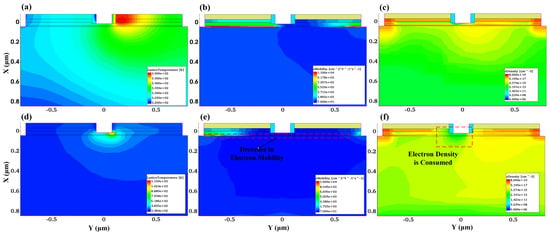
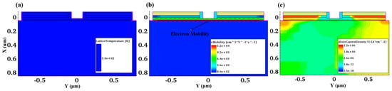
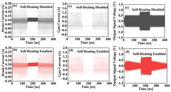
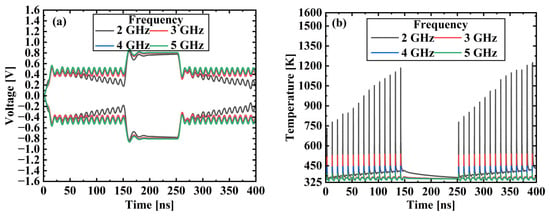
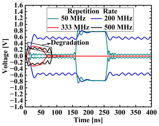
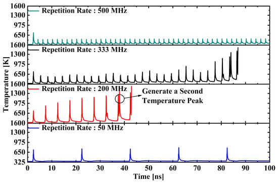
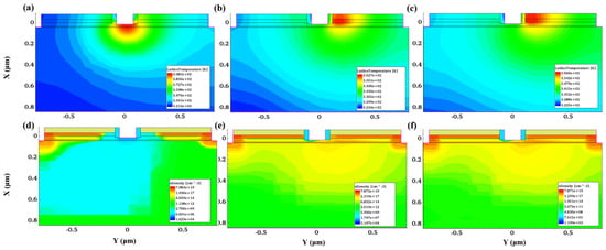
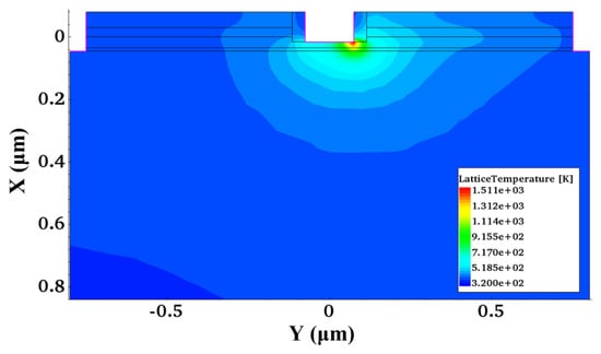
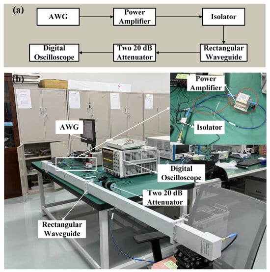
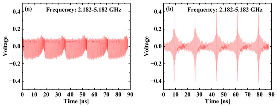
Ultra-short microwave pulses with durations of 1 ns or less can go through a PIN limiter with low attenuation before the limiter responds and can therefore be directly injected into the subsequent low-noise amplifier (LNA). Based on this consideration, this paper reports the first investigation of degradation and damage in the GaAs pseudomorphic high-electron-mobility transistors (pHEMT) LNA induced by high-power ultra-short microwave pulses. The effects of pulse power, frequency, and repetition rate on the degradation and damage mechanisms of the LNA are investigated. The results show that, when exposed to a 45 dBm ultra-short microwave pulse at 2 GHz, the region beneath the transistor gate on the drain side experiences the most rapid burnout within 43 ns at a repetition rate of 200 MHz. Further analysis reveals that the negative half-cycle of the high-power microwave pulse depletes the electron concentration in the transistor. Consequently, excessively high repetition rates of high-power ultra-short microwave pulses are less likely to induce transistor burnout. Furthermore, the gain of the LNA is affected by both the electron concentration and the electron mobility in the transistor. The injected high-power ultra-short microwave pulses disturb the electron concentration, while the temperature rise reduces electron mobility. As a result, the transistor performance degrades, leading to a decrease in the LNA gain.
Full article
(This article belongs to the Special Issue Microwave Passive Components, 3rd Edition)
►▼
Show Figures

Figure 1
Open AccessArticle
Enhancing the Source-Side Transient Response of Logarithmic Double-Spiral Terahertz Photoconductive Antennas Using a Central-Feed-Boundary Tip Array
by
Chao Xu, Shuaiqi Wang, Yu Zhang, He Dong, Jian Gao and Guofeng Wang
Micromachines 2026, 17(9), 1053; https://doi.org/10.3390/mi17091053 - 3 Sep 2026
Abstract
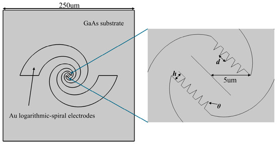
The smooth central feed boundary of a logarithmic double-spiral terahertz photoconductive antenna can limit the spatial overlap between the high-field region and photogenerated carriers, thereby restricting the source-side transient response. We introduced a micrometer-scale tip array along the central feed boundary and investigated
[...] Read more.
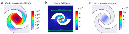
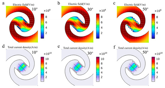
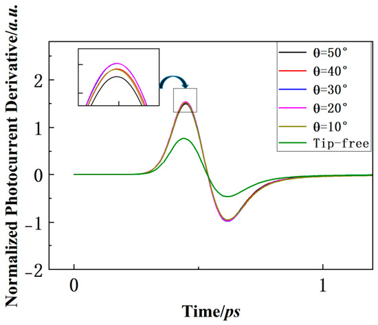
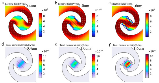
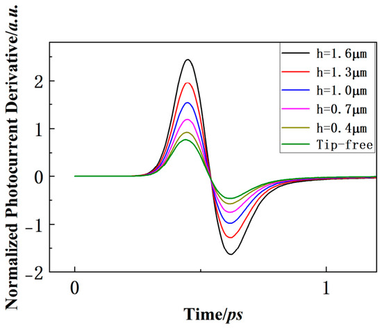
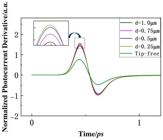
The smooth central feed boundary of a logarithmic double-spiral terahertz photoconductive antenna can limit the spatial overlap between the high-field region and photogenerated carriers, thereby restricting the source-side transient response. We introduced a micrometer-scale tip array along the central feed boundary and investigated the influence of tip apex angle, height, and spacing through a transient semiconductor model in COMSOL Multiphysics. The photocurrent derivative, which is proportional to the emitted terahertz electric field under the transient-current approximation, was adopted as the source-side response metric. The tip array enhanced the response by redistributing the local bias field and bringing the carrier-collection boundary closer to the illuminated region. Within the investigated ranges, tip height produced the strongest response variation, whereas the influence of the apex angle remained limited over 10–50°, and further reducing d from 0.5 to 0.25 μm resulted in only a marginal response improvement. For θ = 30°, h = 1.0 μm, and d = 0.5 μm, the positive-peak and peak-to-peak enhancement ratios reached 100.1% and 103.9%, respectively. These results provide source-side design guidance for parameter selection while qualitatively considering geometric perturbation and fabrication practicality.
Full article
(This article belongs to the Special Issue Advanced Microwave Devices and RF Chips: Design, Microfabrication, and Applications)
►▼
Show Figures

Figure 1
Open AccessArticle
Thermal-Hydraulic Performance Optimization of Open Microchannel Heat Sinks with Integrated Front Triangular Ribs and Secondary Channels
by
Jianlong Gong and Zhongliang Pan
Micromachines 2026, 17(9), 1052; https://doi.org/10.3390/mi17091052 - 3 Sep 2026
Abstract
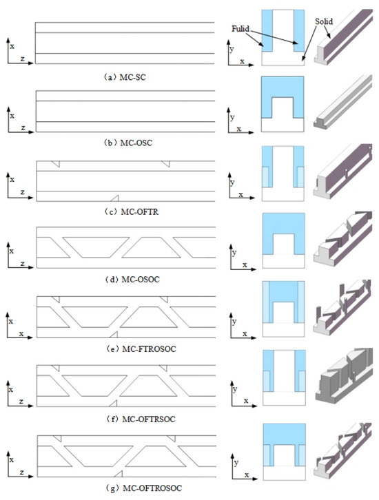
To enhance the comprehensive thermal-hydraulic performance of microchannel heat sinks (MCHS), this work proposed a novel open-type MCHS integrated with front triangular ribs and secondary channels. Firstly, numerical computations were carried out to compare the flow and heat transfer characteristics of seven distinct
[...] Read more.
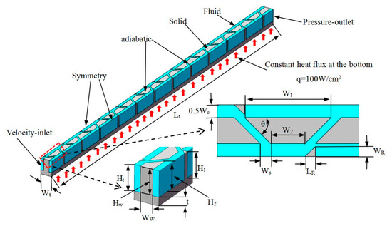
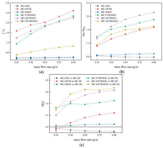
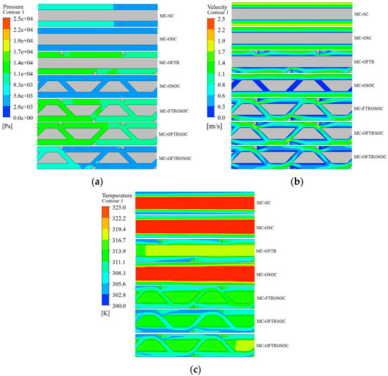
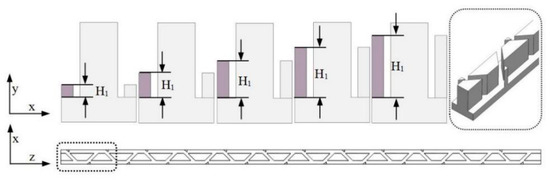
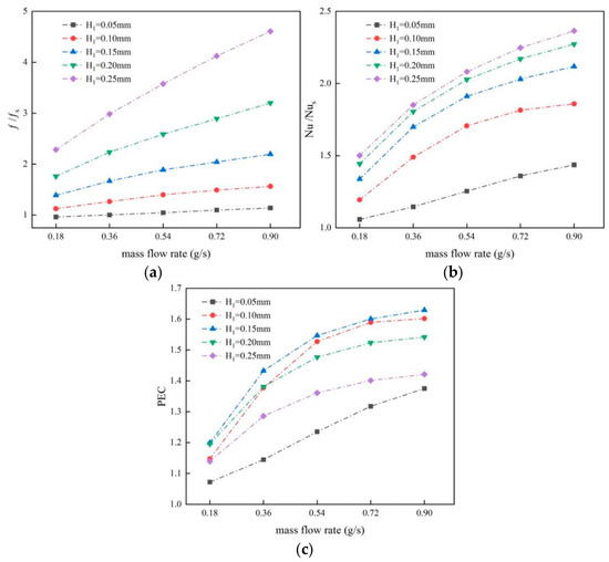
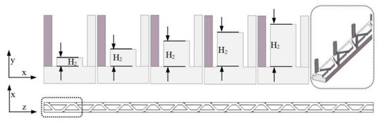
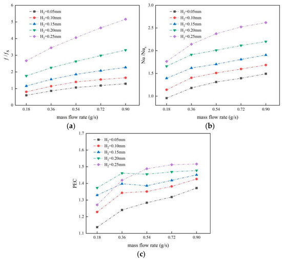
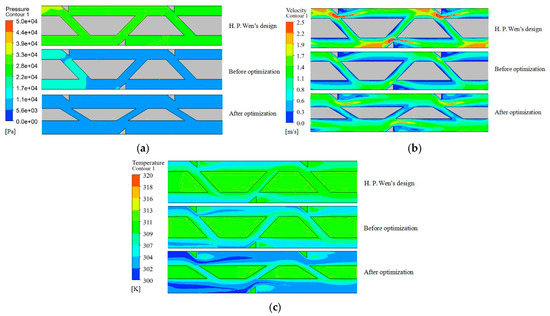
To enhance the comprehensive thermal-hydraulic performance of microchannel heat sinks (MCHS), this work proposed a novel open-type MCHS integrated with front triangular ribs and secondary channels. Firstly, numerical computations were carried out to compare the flow and heat transfer characteristics of seven distinct MCHS configurations, and identify the optimal hybrid geometry consisting of an open microchannel fitted with integrated front triangular ribs and secondary channels. Secondly, the effects of H1 (height of open front triangular ribs) and H2 (height of open secondary channels) on the thermal-hydraulic performance of the MCHS were systematically analyzed. The results revealed that the composite open MCHS obtained its peak performance evaluation criterion (PEC) value at H1 = 0.15 mm and H2 = 0.25 mm from separate single-factor parametric analyses for H1 and H2, at a mass flow rate of 0.9 g/s. Finally, a surrogate model correlating three structural parameters (H1, H2, Ww) with the optimization objective (PEC) was established based on orthogonal test data. This surrogate model was coupled with a genetic algorithm to perform global parameter optimization to maximize PEC. Relative to the original design and the reference geometry in other literature, the optimized design achieved maximum reductions of 15.3% in thermal resistance and 70.9% in pumping power, accompanied by a 55.7% improvement in PEC. This research provides theoretical support for the structural design of high-heat-flux microchannel cooling devices.
Full article
(This article belongs to the Special Issue Emerging Technologies and Applications for Semiconductor Industry, 2nd Edition)
►▼
Show Figures

Figure 1
Open AccessReview
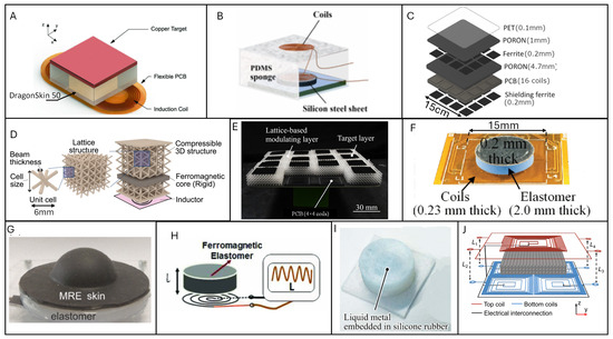
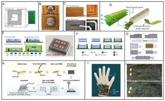
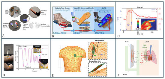
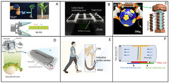
SoftMechanical Inductive Sensors: Principles, Design, and Applications
by
Muhammad Awais, Gayatri Indukumar, Diana Cafiso and Lucia Beccai
Micromachines 2026, 17(9), 1051; https://doi.org/10.3390/mi17091051 - 2 Sep 2026
Abstract
Soft mechanical inductive (SMI) sensors are emerging as a promising solution for advanced robotics, healthcare, and wearable devices, offering high precision, adaptability, and environmental robustness. These sensors leverage coil-based designs to achieve resilience against temperature variations, humidity, and mechanical wear, making them suitable
[...] Read more.
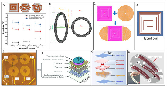
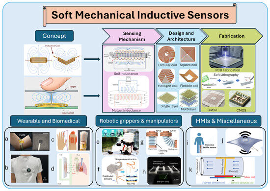
Soft mechanical inductive (SMI) sensors are emerging as a promising solution for advanced robotics, healthcare, and wearable devices, offering high precision, adaptability, and environmental robustness. These sensors leverage coil-based designs to achieve resilience against temperature variations, humidity, and mechanical wear, making them suitable for long-term operation in challenging environments. Existing reviews tend to focus narrowly on specific applications of coil-based inductive sensors, such as soft-robotic tactile sensing or biomedical devices, without systematically comparing design methodologies, fabrication techniques, or broader use cases, thereby lacking a unified perspective on the field. This review addresses this gap by analyzing recent developments in SMI sensors from theoretical concepts and practical design to their use cases. The review focuses on the working principles, design strategies, fabrication techniques, electronic interfaces, and, finally, the applications of coil-based SMI sensors. Key applications in soft robotics, prosthetics, and haptic devices are examined, highlighting the transformative potential of these sensors across diverse domains. Finally, the review discusses critical challenges, including sensitivity optimization, durability, and environmental interference, and outlines future directions to further advance this promising technology.
Full article
(This article belongs to the Special Issue MEMS and NEMS Sensors: Innovations, Applications, and Future Directions in Micro/Nano Technologies)
►▼
Show Figures

Figure 1
Open AccessArticle
Bonding with a Benchtop UV Ozone Cleaner: A Practical Guide to Prepare a Microfluidic Chip
by
Mirjam P. M. Poschmann, Lucas Holtorf, Igor Titov, Nahomy M. Lizarde, Thomas Strunskus and Martina Gerken
Micromachines 2026, 17(9), 1050; https://doi.org/10.3390/mi17091050 - 2 Sep 2026
Abstract
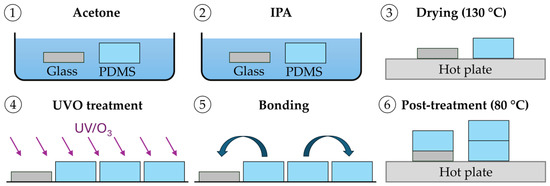
This study describes a procedure for preparing microfluidic chips made from polydimethylsiloxane (PDMS) layers. It uses an Ossila UV ozone cleaner for surface activation instead of the more common oxygen plasma treatment. The process is limited to PDMS@PDMS bonding, and it can be
[...] Read more.
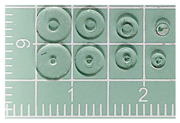
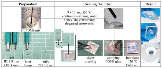
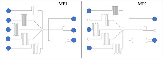
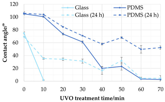
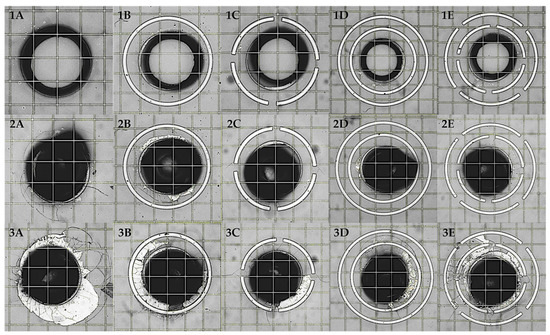
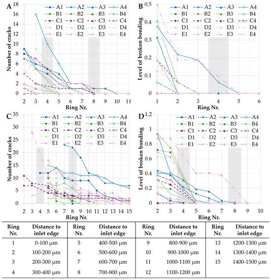
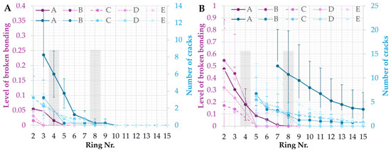
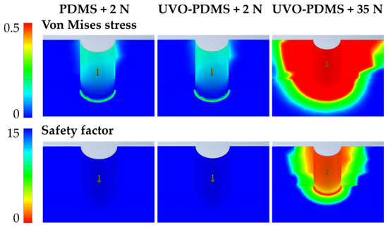
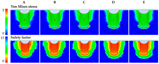
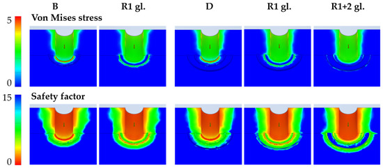
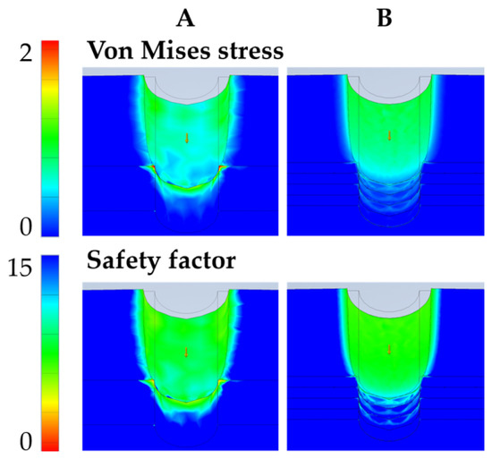
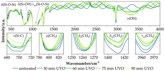
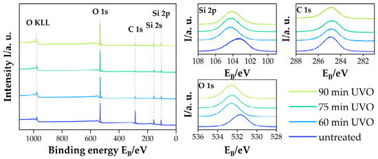
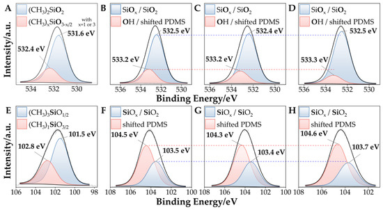
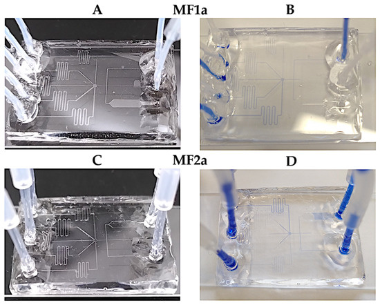
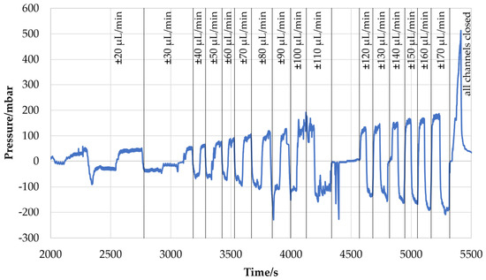
This study describes a procedure for preparing microfluidic chips made from polydimethylsiloxane (PDMS) layers. It uses an Ossila UV ozone cleaner for surface activation instead of the more common oxygen plasma treatment. The process is limited to PDMS@PDMS bonding, and it can be used when a low-cost procedure for a small number of microfluidic chips is required or when an oxygen plasma etcher is unavailable. The challenges of this process arise from the slight hardening of the PDMS surface when it is activated for at least 70 min, which is necessary for reliable bonding. Activation of the surface is confirmed by contact angle measurements. In a static simulation and lab tests, it is demonstrated that damage resulting from this hardening in conjunction with careless handling of the microfluidic chip is mitigated by incorporating predetermined break structures and using tubes with an outer diameter that is smaller than the inlets. Additionally, pre-polymerized PDMS glue and PDMS seals are suggested to ensure that the tubes are properly sealed. A burst test in air was performed to demonstrate the stability of the bonding and gluing. IR and XPS measurements were performed to investigate surface and bulk changes due to the treatment. To demonstrate the concept, six microfluidic chips were prepared and tested, achieving flow rates of at least 170 µL/min at ±180 mbar. Bonding remains stable up to a pressure of approximately 428 ± 60 mbar.
Full article
(This article belongs to the Special Issue Advances in Microfluidic Chips for Chemical and Biomedical Applications, 2nd Edition)
►▼
Show Figures

Figure 1
Open AccessArticle
Hardware–Algorithm Co-Optimization of Weight-Update Protocols in Oxide-Based Synaptic Transistor Arrays for Neuromorphic Systems
by
Yixin Cao, Jingsong Xia, Xiangyi Ding, Xin Wang, Jin Liu and Canhua Xu
Micromachines 2026, 17(9), 1049; https://doi.org/10.3390/mi17091049 - 2 Sep 2026
Abstract
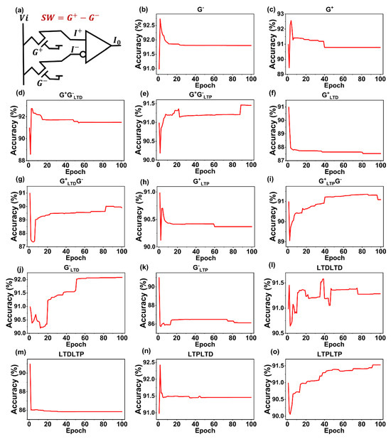
The transition from single-device characterization to array-level simulation remains a critical challenge in the development of three-terminal synaptic transistors for neuromorphic computing, as most existing simulation studies either extract parameters from a single representative device and apply them uniformly, or rely on weight-update
[...] Read more.
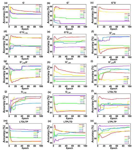
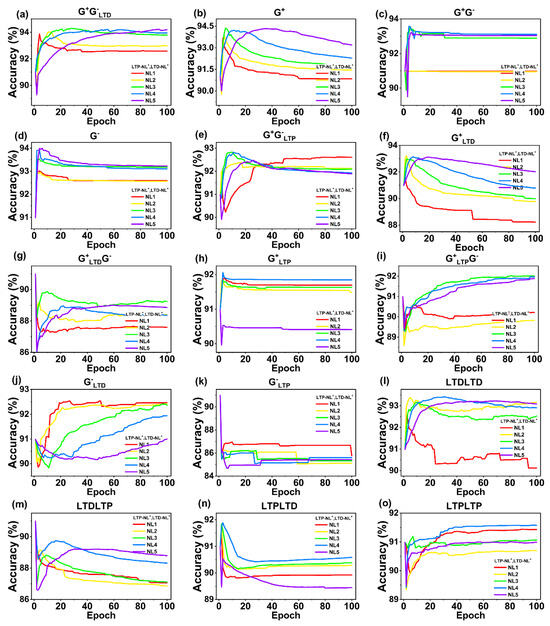
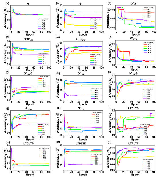
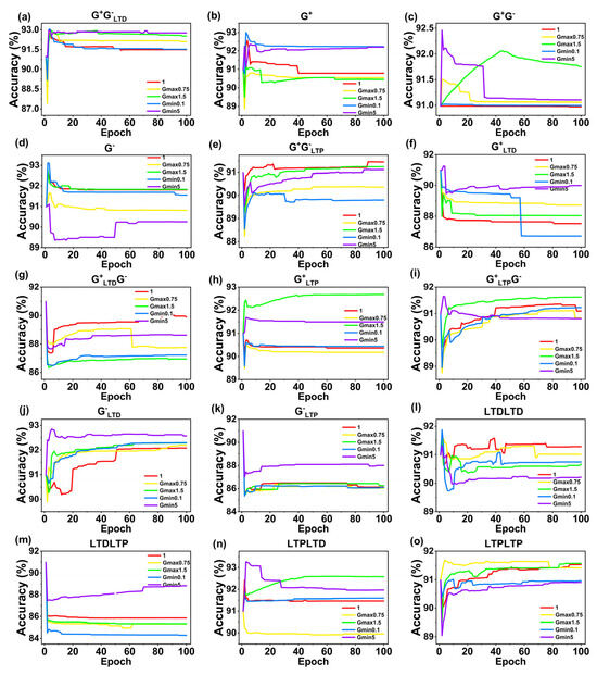
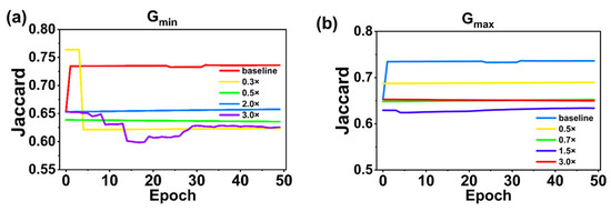
The transition from single-device characterization to array-level simulation remains a critical challenge in the development of three-terminal synaptic transistors for neuromorphic computing, as most existing simulation studies either extract parameters from a single representative device and apply them uniformly, or rely on weight-update strategies originally designed for two-terminal memristors. Here, we establish an experimentally calibrated behavioral simulation framework based on differential conductance-pair mapping (W = G+ − G−, where G+ and G− denote the conductances of the positive and negative devices of each pair), integrating exponential long-term potentiation/depression (LTP/LTD) update rules with a posteriori screening mechanism (isValid) to systematically investigate how update polarity, step size, nonlinearity, and conductance boundaries regulate network computational efficiency. Through comprehensive simulation on the Neural Circuit Policies network, we demonstrate that the update direction must strictly align with the matrix’s role: the G− channel requires unidirectional long-term depression inhibition, while the G+ channel can be frozen or bidirectionally updated. The optimal G−LTD and G+G−LTD strategies achieve accuracies of 0.9208 and 0.9481, respectively. Furthermore, we reveal a unique nonlinear gain effect under long-term depression > 0, where accuracy increases monotonically with nonlinearity level up to 0.9419. Device specification criteria are established: LTP-dominant updates favor large Gmax, while LTD-dominant updates favor high Gmin, with the G−LTD and G+G−LTD strategies showing accuracy fluctuations within ±0.005 across the tested boundary variations. Finally, the array-level implementation is validated through a functional-correctness check and device-parameter ablation experiments on a 23,715-weight array (47,430 differential conductance elements). This work provides an experimentally calibrated behavioral simulation platform and concrete algorithm-hardware co-design guidelines for future neuromorphic hardware, prioritizing synaptic devices with long-term depression > 0, a moderately elevated Gmin, and asymmetric resource allocation toward LTD-side optimization.
Full article
(This article belongs to the Section D1: Semiconductor Devices)
►▼
Show Figures

Figure 1
Journal Menu
► ▼ Journal Menu-
- Micromachines Home
- Aims & Scope
- Editorial Board
- Reviewer Board
- Topical Advisory Panel
- Early Career Editorial Board
- Instructions for Authors
- Special Issues
- Topics
- Sections & Collections
- Article Processing Charge
- Indexing & Archiving
- Editor’s Choice Articles
- Most Cited & Viewed
- Journal Statistics
- Journal History
- Journal Awards
- Society Collaborations
- Conferences
- Editorial Office
Journal Browser
► ▼ Journal BrowserHighly Accessed Articles
Latest Books
E-Mail Alert
News
9 September 2026
Meet Us at the 2nd National Conference on Analytical Science and Instrumentation, 30 October–2 November 2026, Wuhan, China
8 September 2026
Meet Us at the 4th International Conference on AI Sensors and Transducers (AIS 2027), 29 July–3 August 2027, Kunming, Yunnan, China
Topics
Topic in
Electronics, Fluids, Machines, Micromachines, Applied Sciences
Micro-Mechatronic Engineering, 2nd Edition
Topic Editors: Teng Zhou, Antonio F. MiguelDeadline: 31 October 2026
Topic in
Applied Sciences, Energies, Fluids, Micromachines, Processes
Enhanced Heat Transfer and Advanced Energy Conversion Technology, 2nd Edition
Topic Editors: Feng Zhang, Yong LiDeadline: 30 November 2026
Topic in
Designs, Electronics, Energies, Micromachines
Power Electronics Converters, 2nd Edition
Topic Editors: Mohsin Jamil, Yuanmao Ye, Tomasz PajchrowskiDeadline: 31 December 2026
Topic in
Foods, Materials, Polymers, Safety, Sensors, Toxics, Micromachines
Development of Rapid Detection Methods for Foodborne Micro/Trace Hazardous Substances
Topic Editors: Bo Zhang, Yukun YangDeadline: 31 January 2027
Conferences
Special Issues
Special Issue in
Micromachines
Advances in Pressure Sensors
Guest Editor: Xudong FangDeadline: 15 September 2026
Special Issue in
Micromachines
Machine Learning in Microfluidics
Guest Editor: Hyungkook JeonDeadline: 15 September 2026
Special Issue in
Micromachines
Advancing MEMS/MOEMS Sensors: AI-Driven Optimization and Emerging Applications
Guest Editor: Qianbo LuDeadline: 20 September 2026
Special Issue in
Micromachines
Emerging Devices and Technologies in BioMEMS for Biomarker Detection
Guest Editors: Jianwei Zhong, Minhui Liang, Ye AiDeadline: 20 September 2026
Topical Collections
Topical Collection in
Micromachines
Lab-on-a-Chip
Collection Editors: Jeong-Bong Lee, Ning Xue, Xiwei Huang
Topical Collection in
Micromachines
Micromixers: Analysis, Design and Fabrication
Collection Editor: Kwang-Yong Kim
Topical Collection in
Micromachines
Microdevices and Applications Based on Advanced Glassy Materials
Collection Editors: Giancarlo Righini, Luigi Sirleto, Francesco Enrichi