




Journal Description
Journal of Low Power Electronics and Applications
is an international, peer-reviewed, open access journal on low power electronics published quarterly online by MDPI.
- Open Access— free for readers, with article processing charges (APC) paid by authors or their institutions.
- High Visibility: indexed within Scopus, ESCI (Web of Science), Inspec, and other databases.
- Rapid Publication: manuscripts are peer-reviewed and a first decision is provided to authors approximately 21.8 days after submission; acceptance to publication is undertaken in 4.8 days (median values for papers published in this journal in the first half of 2026).
- Journal Rank: CiteScore - Q2 (Electrical and Electronic Engineering)
- Recognition of Reviewers: Reviewers whose reports are timely and of high quality receive an APC discount voucher for a future publication in an MDPI journal. Become a reviewer.
- Journal Cluster of Electronic Engineering and Hardware Systems: Chips, Electronics, Hardware, Journal of Low Power Electronics and Applications, Microelectronics and Microwave.
Impact Factor:
1.7 (2025);
5-Year Impact Factor:
1.7 (2025)
Latest Articles
Versat-AI: An ONNX-to-SoC Compiler for Model-Agnostic CGRA Edge Inference
J. Low Power Electron. Appl. 2026, 16(3), 36; https://doi.org/10.3390/jlpea16030036 - 4 Sep 2026
Abstract
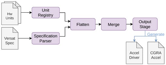
Edge inference on resource-constrained embedded nodes demands accelerators that are energy-efficient and compact. This paper presents Versat-AI, an open-source compiler that accepts a standard Open Neural Network Exchange (ONNX) model and generates a complete, synthesisable RISC-V System-on-Chip (SoC) with an embedded CGRA accelerator.
[...] Read more.
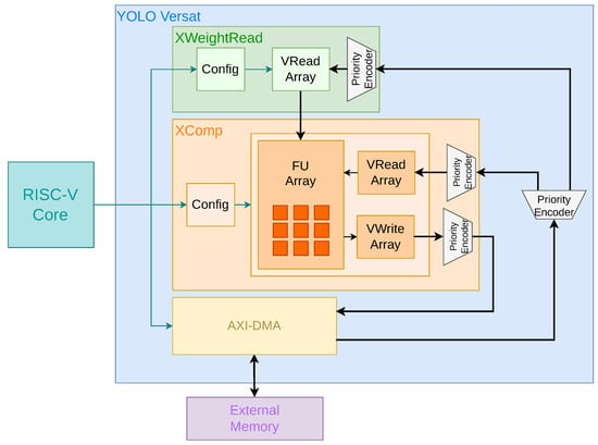
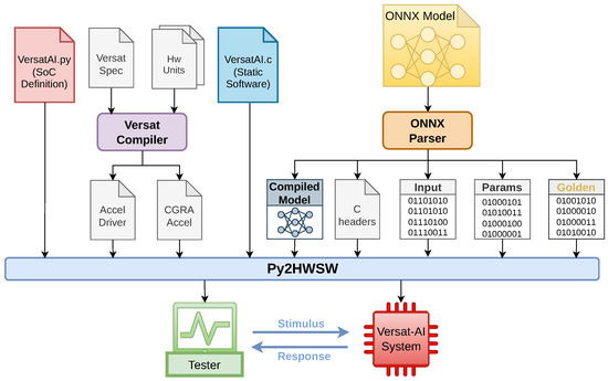
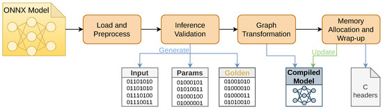
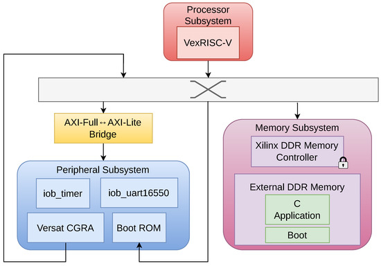
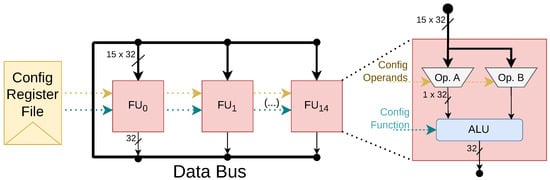
Edge inference on resource-constrained embedded nodes demands accelerators that are energy-efficient and compact. This paper presents Versat-AI, an open-source compiler that accepts a standard Open Neural Network Exchange (ONNX) model and generates a complete, synthesisable RISC-V System-on-Chip (SoC) with an embedded CGRA accelerator. The key innovation is applying a known hardware merge strategy to collapse structurally compatible neural network operators into a physical CGRA instance. The Versat-AI compiler also derives memory-mapped interconnects, firmware drivers, and RISC-V application software co-generated by the Py2HWSW SoC framework, eliminating the manual hardware/software co-design effort that previously tied this accelerator’s own design lineage to a single target network. The next phase of the project is to extend this same automatic derivation from sizing the operator vocabulary to sizing per-operator parallel instancing and bandwidth, following the bandwidth-matched scaling principle already demonstrated, by hand, in this accelerator’s own design lineage. The current phase of the project has succeeded in creating a sound automation flow that produces an accelerator that maps each operator onto a single physical datapath instance and occupies 8763 LUTs, 9833 flip-flops, 4 DSPs, and 202 BRAMs on a Xilinx Kintex UltraScale field-programmable gate array (FPGA)—a footprint unchanged across all evaluated models regardless of size—and draws 0.65 W (1.96 W for the complete SoC including the DDR4 controller, by Vivado post-implementation power estimation), achieving to speedup over the software-only baseline produced by the same flow on four MLPerf Tiny benchmark tasks. The paper further examines the design choices that delimit this first phase—single-precision arithmetic, a single datapath instance per operator, and the block-RAM cost of the accelerator’s streaming buffers—and sets out the path to quantised integer support and parallel operator instancing. A condensed account of the two-decade lineage of reconfigurable accelerators and open-source SoC platforms that motivated Versat-AI’s design is also given.
Full article
(This article belongs to the Special Issue 15th Anniversary of Journal of Low Power Electronics and Applications)
►
Show Figures
Open AccessArticle
FPGA Implementation of a Low-Power VLSI Architecture for Medical Image Scaling
by
Mrinalini Joshi-Pangaonkar and Pratibha Shingare
J. Low Power Electron. Appl. 2026, 16(3), 35; https://doi.org/10.3390/jlpea16030035 - 1 Sep 2026
Abstract
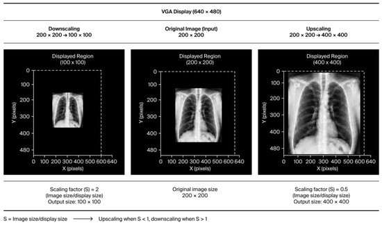
This paper presents an FPGA (Field-Programmable Gate Array) implementation of a low-power VLSI (Very Large-Scale Integration) architecture for medical image scaling in portable diagnostic systems. The proposed architecture employs bilinear interpolation optimized through FSM (Finite-State-Machine)-based control, a clock-enable technique, and selective block activation
[...] Read more.
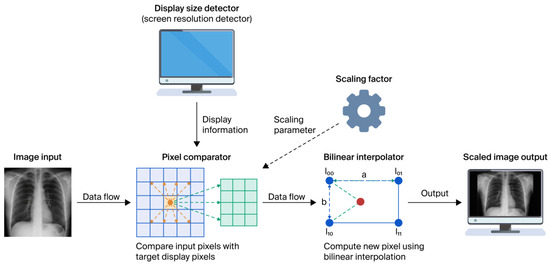
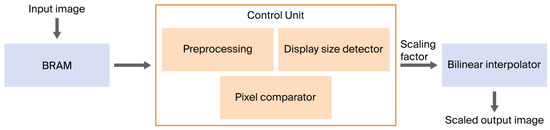
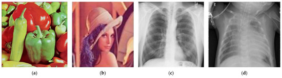
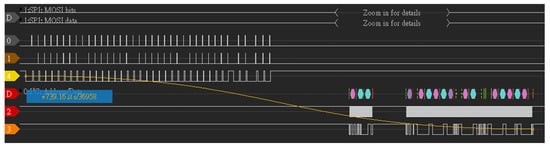
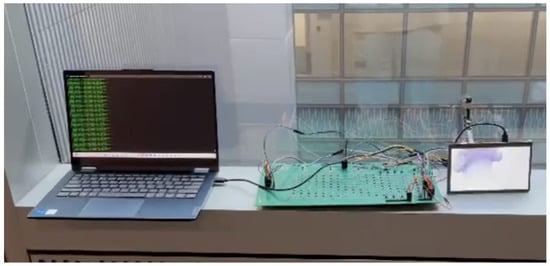
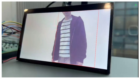
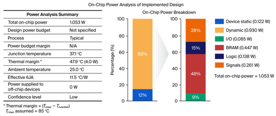
This paper presents an FPGA (Field-Programmable Gate Array) implementation of a low-power VLSI (Very Large-Scale Integration) architecture for medical image scaling in portable diagnostic systems. The proposed architecture employs bilinear interpolation optimized through FSM (Finite-State-Machine)-based control, a clock-enable technique, and selective block activation to reduce switching activity and dynamic power consumption while preserving image quality. The architecture is described in Verilog HDL, synthesized using Vivado 2024.1, and implemented on the Xilinx Zynq-7000-based ZedBoard platform. A controlled post-implementation power analysis on the same FPGA platform demonstrates a reduction in estimated total on-chip power from 3.739 W for the unoptimized baseline architecture to 1.053 W for the optimized architecture, corresponding to an approximately 71.8% reduction. The system supports multiple operational modes, including original image display, grayscale conversion, Sobel X filtering, and Sobel Y filtering, providing enhanced diagnostic flexibility. Quantitative assessment of the exemplary X-ray Image 1 yielded PSNR (Peak Signal-to-Noise Ratio) of 42.97 dB and SSIM (Structural Similarity Index) of 0.9557, demonstrating satisfactory image-quality preservation after scaling. The proposed architecture demonstrates the feasibility of low-power FPGA-based medical image scaling for portable diagnostic and telemedicine imaging systems, offering an effective balance between energy efficiency and image fidelity.
Full article
(This article belongs to the Special Issue 15th Anniversary of Journal of Low Power Electronics and Applications)
►▼
Show Figures

Figure 1
Open AccessArticle
A Priority-Aware Piggybacking-Based Energy-Efficient MAC Protocol Using Bit Mapping
by
Tanvi Mishra, Manoj Tolani, Gaurav Suman, Himanshu Chaudhary, Pankaj Kumar and Simmi Sharma
J. Low Power Electron. Appl. 2026, 16(3), 34; https://doi.org/10.3390/jlpea16030034 - 1 Sep 2026
Abstract
Battery-powered IoT sensor nodes require energy-efficient Medium Access Control (MAC) protocols to extend network lifetime while supporting priority-sensitive traffic. This paper proposes a Priority-Aware Packet Aggregation/Piggybacking-Based (Priority + Packet Aggregation) Hybrid Energy-Efficient MAC ( A-HMAC) protocol that integrates bit-mapped priority signaling
[...] Read more.
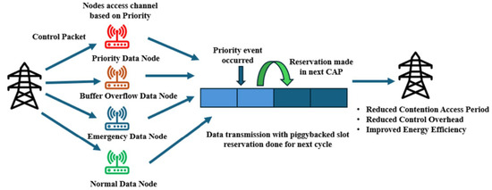
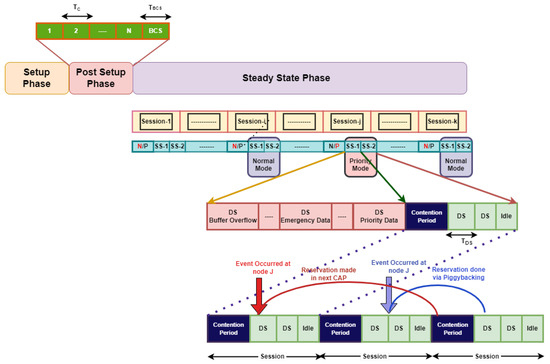
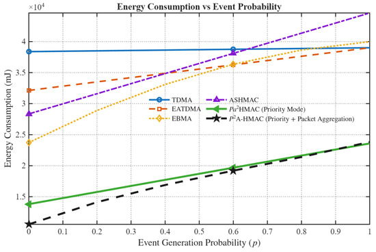
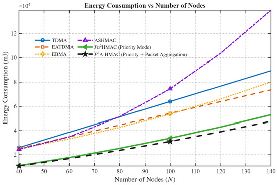
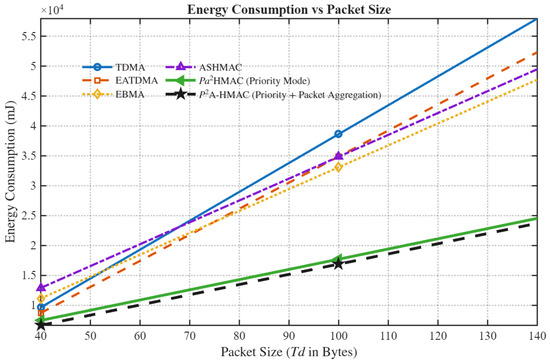
Battery-powered IoT sensor nodes require energy-efficient Medium Access Control (MAC) protocols to extend network lifetime while supporting priority-sensitive traffic. This paper proposes a Priority-Aware Packet Aggregation/Piggybacking-Based (Priority + Packet Aggregation) Hybrid Energy-Efficient MAC ( A-HMAC) protocol that integrates bit-mapped priority signaling with lightweight packet aggregation/piggybacking to reduce control overhead. The protocol classifies traffic into emergency, buffer-overflow, priority, and normal categories, providing guaranteed access to delay-sensitive data while minimizing radio activity, idle listening, and contention. A mathematical energy model is developed for both priority- and contention-based operations. MATLAB-based evaluation demonstrates that A-HMAC consistently achieves lower energy consumption than TDMA, EA-TDMA, ASHMAC, E-BMA, and A-HMAC across varying network sizes, packet sizes, and event-generation probabilities. The proposed protocol provides substantial energy savings, particularly in large-scale and moderate-traffic networks, while maintaining priority-aware communication and QoS, making it suitable for low-power IoT and wireless sensor network applications.
Full article
(This article belongs to the Special Issue Sustainable Wireless Sensor Networks: Recent Trends and Advances)
►▼
Show Figures

Graphical abstract
Open AccessReview
Energy-Aware Physical Unclonable Functions: From Physical Entropy Sources to MRAM-Based Low-Power Hardware Roots of Trust
by
Jian Yang and Yanfeng Jiang
J. Low Power Electron. Appl. 2026, 16(3), 33; https://doi.org/10.3390/jlpea16030033 - 31 Aug 2026
Abstract
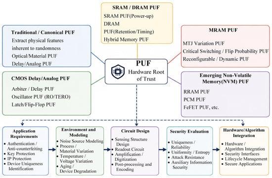
Physical unclonable functions (PUFs) convert device-specific physical variations into responses for chip identity, key reconstruction, secure boot, and hardware roots of trust. This review examines the complete PUF chain from entropy generation and response digitization to stabilization, post-processing, deployment, security evaluation, and low-power
[...] Read more.
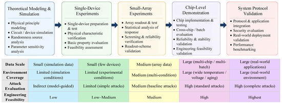
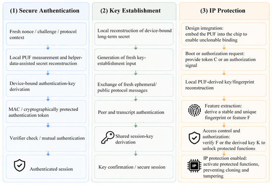
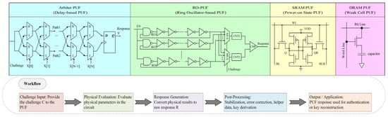
Physical unclonable functions (PUFs) convert device-specific physical variations into responses for chip identity, key reconstruction, secure boot, and hardware roots of trust. This review examines the complete PUF chain from entropy generation and response digitization to stabilization, post-processing, deployment, security evaluation, and low-power implementation. Mature CMOS delay, SRAM, and DRAM PUFs are treated as engineering baselines, while representative emerging-memory PUFs provide comparison points for a MRAM-centered analysis. The main focus is placed on MRAM PUFs, including static MTJ variation, stochastic STT/SOT switching, response digitization and stabilization, reconfigurability, magnetic-specific attack surfaces, and system integration. The main contents include MRAM-PUF energy costs across device operation, raw-response generation, response stabilization, key reconstruction, and complete authentication. This cross-layer perspective distinguishes cell-level read/write energy from repeated sampling, reliable-bit-selection, ECC/KDF, controller, retry, and reconfiguration overheads. MRAM offers distinctive features including non-volatility, high endurance, and stochastic switching behavior. Their system-level energy benefits are treated as application-dependent and should be evaluated at the complete transaction level.
Full article
(This article belongs to the Special Issue Feature Reviews on Emerging Topics in Low-Power Electronics Across the Design Stack)
►▼
Show Figures

Figure 1

Open AccessArticle
Hybrid Filamentary Switching in Fe2O3—Incorporated TiO2 Memristors for Memory and Neuromorphic Computing Application
by
Dwipak Prasad Sahu
J. Low Power Electron. Appl. 2026, 16(3), 32; https://doi.org/10.3390/jlpea16030032 - 12 Aug 2026
Abstract
Memristive devices have emerged as promising candidates for next-generation non-volatile memory and neuromorphic computing systems owing to their simple device architecture, low power consumption, and capability for analog conductance modulation. In this work, Fe2O3-incorporated TiO2 thin films were
[...] Read more.
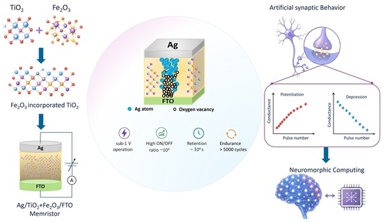
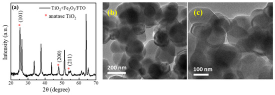
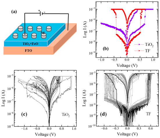
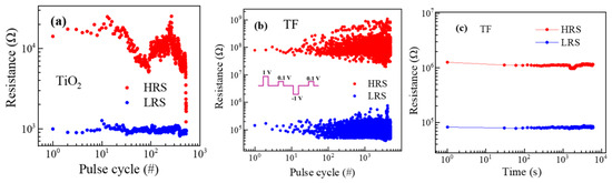
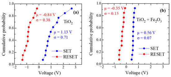
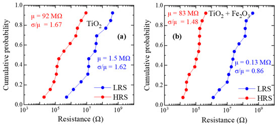
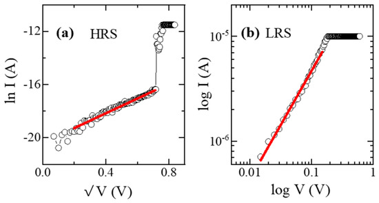
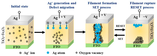
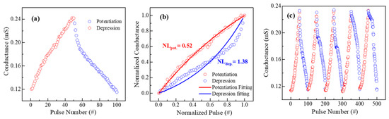
Memristive devices have emerged as promising candidates for next-generation non-volatile memory and neuromorphic computing systems owing to their simple device architecture, low power consumption, and capability for analog conductance modulation. In this work, Fe2O3-incorporated TiO2 thin films were employed as the active switching layer to investigate their resistive switching and artificial synaptic characteristics. The fabricated Ag/TiO2 + Fe2O3/FTO device exhibits stable switching performance with a low operating voltage of approximately ±0.6 V, a large ON/OFF ratio of ~103, retention of nearly 104 s, and endurance over 5000 pulse cycles, representing a significant improvement compared with pristine TiO2 devices. Electrical transport analysis demonstrates Schottky emission-dominated conduction in the high-resistance state and Ohmic conduction in the low-resistance state. Furthermore, analog switching behavior was achieved by operating the device under a higher compliance current, demonstrating gradual conductance modulation and synaptic weight update characteristics, indicating the potential of the device for neuromorphic applications. These results demonstrate that Fe2O3 incorporation provides an effective approach for simultaneously enhancing memory performance and synaptic functionality in TiO2-based memristors, highlighting their potential for future memory and neuromorphic computing applications.
Full article
(This article belongs to the Special Issue Computing with Memories—Scaling in the Era of Big AI)
►▼
Show Figures

Graphical abstract
Open AccessArticle
Low-Power IGZO TFTs with Improved Positive Bias Stability via Atomic Layer Deposition-Based H2O Treatment
by
Kai-Ting Huang, You-Wen Fan, Jung-Yi Lin, Chien-Lung Chen, Yen-Chih Yeh, Yu-Chen Ou, Li-Chen Lin, Yu-Hsien Lin, Guang-Li Luo, Yung-Chun Wu and Fu-Ju Hou
J. Low Power Electron. Appl. 2026, 16(3), 31; https://doi.org/10.3390/jlpea16030031 - 10 Aug 2026
Abstract
In this work, a plasma-free atomic layer deposition (ALD)-based H2O post-treatment method is proposed to precisely modulate hydrogen-related (H-related) traps in indium gallium zinc oxide (IGZO) thin-film transistors (TFTs) by the number of H2O treatment cycles. Under the optimized
[...] Read more.
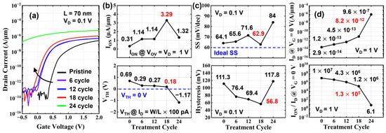
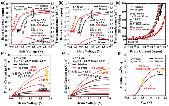
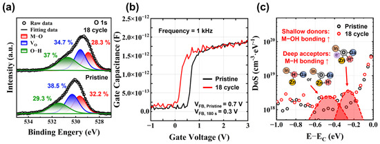
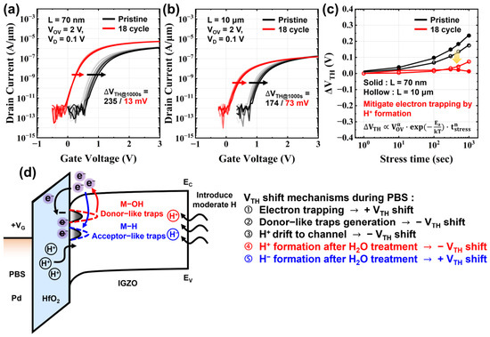
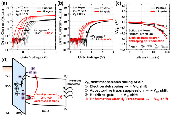
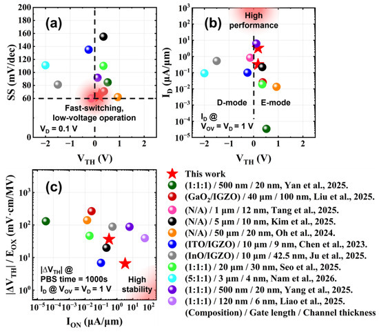
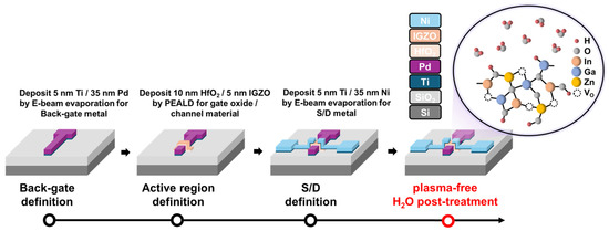
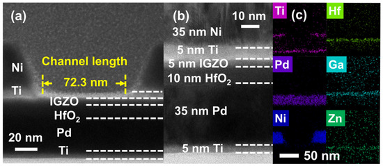
In this work, a plasma-free atomic layer deposition (ALD)-based H2O post-treatment method is proposed to precisely modulate hydrogen-related (H-related) traps in indium gallium zinc oxide (IGZO) thin-film transistors (TFTs) by the number of H2O treatment cycles. Under the optimized condition, the scaled device with a channel length of 70 nm exhibits a near-ideal subthreshold swing of 62.9 mV/dec, a low threshold voltage (VTH) of 0.18 V, an acceptable static leakage current, and a high drive current of 3.29 μA/μm at an overdrive voltage and drain voltage of 1 V. In addition, the treated device shows only a 13 mV of VTH shift after 1000 s positive bias stress (PBS), corresponding to a 94% improvement compared with the pristine device. These improvements are attributed to the introduction of two different polarities of hydrogen-related traps after H2O treatment. Furthermore, the influence of H-related traps on bias stability and the mechanisms responsible for VTH shift are systematically clarified. These results establish that an optimized hydrogen incorporation window that maximizes the beneficial effects while balancing severe hydrogen-induced degradation caused by excessive hydrogen incorporation. Consequently, scaled IGZO TFTs with fast switching, low-power operation, high performance, and high reliability can be achieved, providing strong potential for back-end-of-line (BEOL)-compatible electronics and monolithic three-dimensional integrated applications.
Full article
(This article belongs to the Special Issue 15th Anniversary of Journal of Low Power Electronics and Applications)
►▼
Show Figures

Figure 1
Open AccessArticle
Sensorless Current Estimation in Piezoelectric Energy Harvesting Networks Using a Takagi–Sugeno Fuzzy System
by
Joel Artemio Morales-Viscaya, Martin Moreno, Alberto Traslosheros-Michel and H. J. Vergara-Hernández
J. Low Power Electron. Appl. 2026, 16(3), 30; https://doi.org/10.3390/jlpea16030030 - 7 Aug 2026
Abstract
This paper proposes a sensorless current estimation method for piezoelectric energy harvesting (PEH) systems using a first-order Takagi–Sugeno fuzzy system. Unlike invasive current sensing, the proposed estimator uses only non-invasive measurements: output voltage , its derivative , and
[...] Read more.
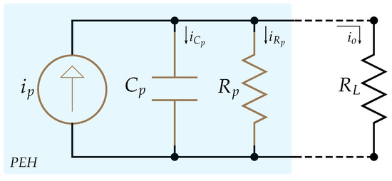
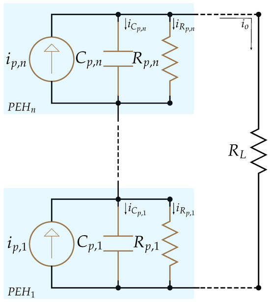
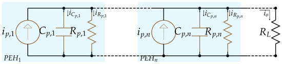
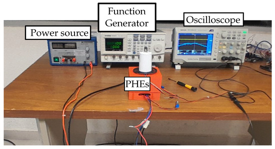
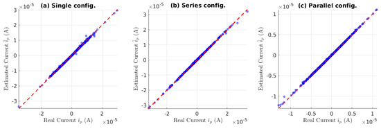
This paper proposes a sensorless current estimation method for piezoelectric energy harvesting (PEH) systems using a first-order Takagi–Sugeno fuzzy system. Unlike invasive current sensing, the proposed estimator uses only non-invasive measurements: output voltage , its derivative , and load resistance . The fuzzy rules are initialized directly from the physical equivalent circuit parameters and trained via the ANFIS on a large-scale dataset (78 million samples). The proposed model achieves a mean coefficient of determination (95% CI: [0.99989, 0.99991]), root mean square error A, mean absolute percentage error MAPE = 2.51% (95% CI: [1.98, 3.04]%), and fitness FIT = 98.98%—outperforming multiple linear regression and MAPE = 116.25%) and a shallow neural network with 211 parameters and MAPE = 13.85%) despite having only 170 trainable parameters. Unlike black-box neural networks, the fuzzy model provides interpretable rules whose consequent parameters map directly to physical quantities (effective capacitance and leakage conductance ). The low computational footprint (170 parameters, <5 μs inference, and ≈1.4 kB of memory) makes it suitable for real-time deployment on low-power microcontrollers. These results demonstrate the viability of the proposed approach under controlled laboratory conditions for the single, series, and parallel PEH configurations considered. This work establishes that physically informed fuzzy modeling is a viable, interpretable, and efficient alternative to deep learning for sensorless monitoring in low-power energy harvesting systems.
Full article
(This article belongs to the Special Issue 15th Anniversary of Journal of Low Power Electronics and Applications)
►▼
Show Figures

Graphical abstract
Open AccessArticle
A Tunable CMOS Sine Waveform Generator for On-Chip Impedance Spectroscopy
by
Erick Iván Barros de la Cruz, Juan David Salazar Cardona, Maria Teresa Sanz-Pascual, Nicolás Medrano and Belén Calvo
J. Low Power Electron. Appl. 2026, 16(3), 29; https://doi.org/10.3390/jlpea16030029 - 4 Aug 2026
Abstract
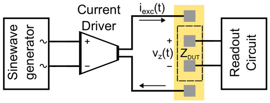
This paper presents a low-power fully integrated sine signal generator for on-chip bioimpedance spectroscopy applications. The circuit is based on a relaxation oscillator, which generates a triangular signal, followed by a sixth-order Gm-C bandpass filter (BPF) that linearizes the waveform. Both blocks, designed
[...] Read more.
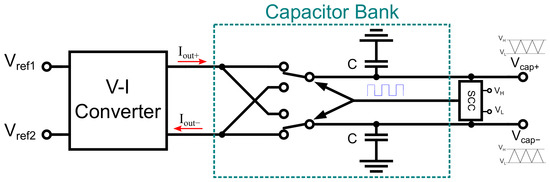
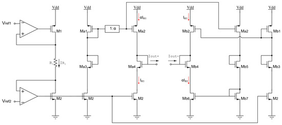
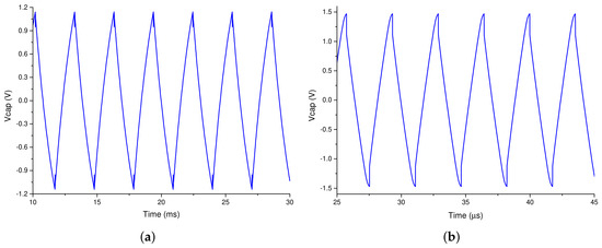
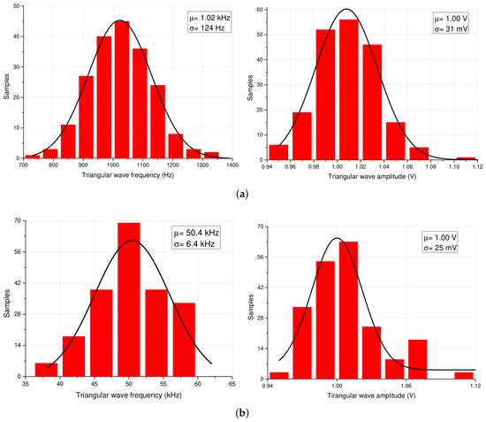
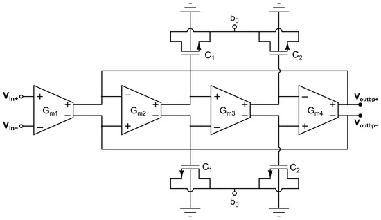
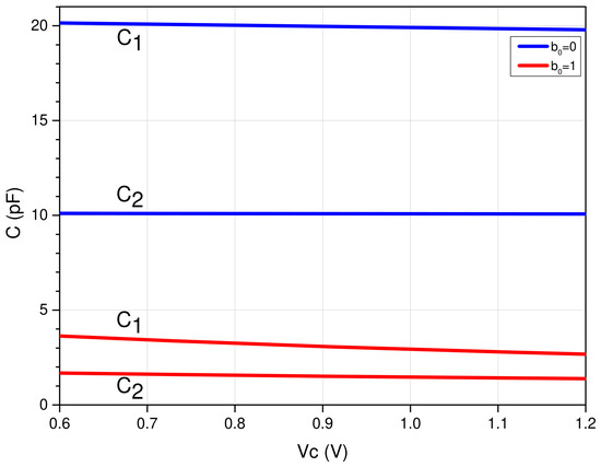
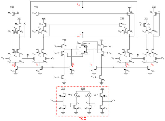
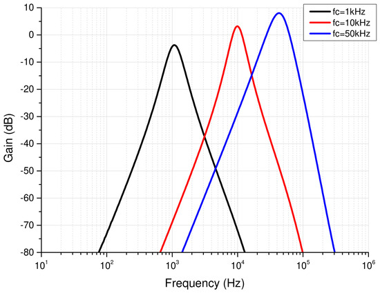
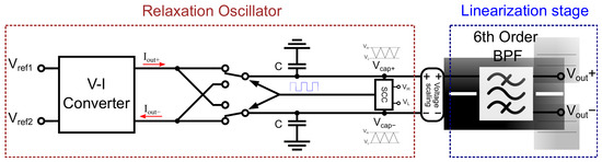
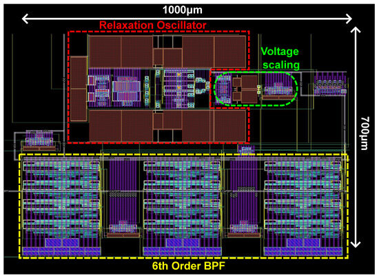
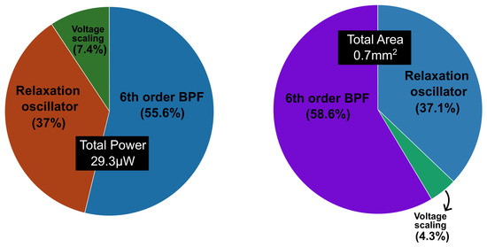
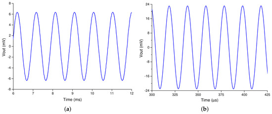
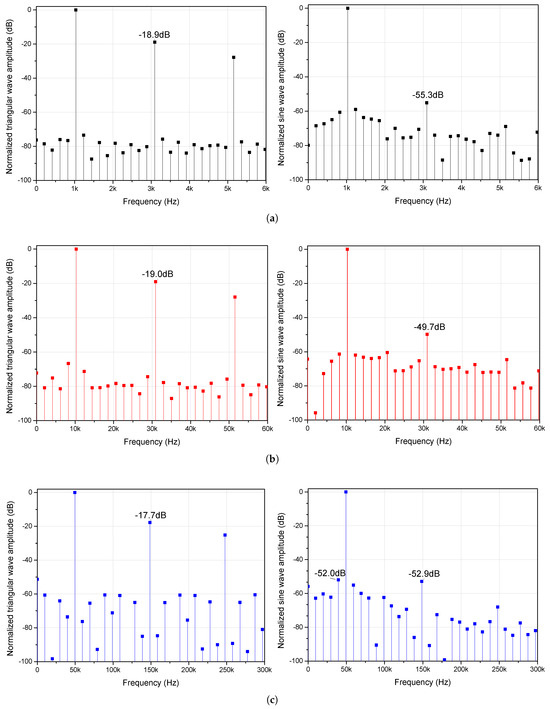
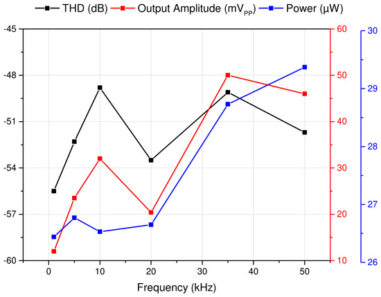
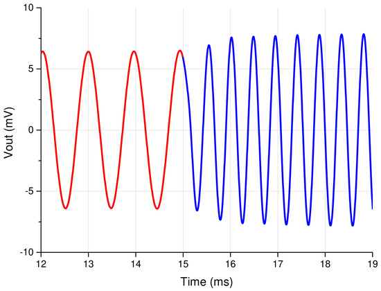
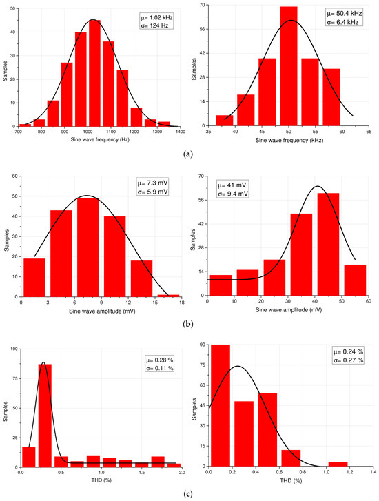
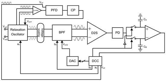
This paper presents a low-power fully integrated sine signal generator for on-chip bioimpedance spectroscopy applications. The circuit is based on a relaxation oscillator, which generates a triangular signal, followed by a sixth-order Gm-C bandpass filter (BPF) that linearizes the waveform. Both blocks, designed in a 0.18 m CMOS process with 1.8 V supply, make use of a current division technique to generate low-frequency signals without requiring high-valued passive components. The relaxation oscillator features an extended frequency tuning range from 300 Hz to 300 kHz, controlled via a tuning current and a digital capacitor bank. The sine output waveform spans from 1 kHz to 50 kHz, and exhibits a −48.8 dB total harmonic distortion at 10 kHz with 18 mV amplitude. The overall system area is 0.7 and the power consumption is lower than 30 W.
Full article
(This article belongs to the Topic Advanced Integrated Circuit Design and Application)
►▼
Show Figures

Figure 1

Open AccessArticle
Low Power Reconfigurable Neuromorphic Architecture by Sparsely Connected Spiking Neural Networks for Edge Applications
by
Alishba Masood and Muhammad Khurram
J. Low Power Electron. Appl. 2026, 16(3), 28; https://doi.org/10.3390/jlpea16030028 - 2 Aug 2026
Abstract
►▼
Show Figures
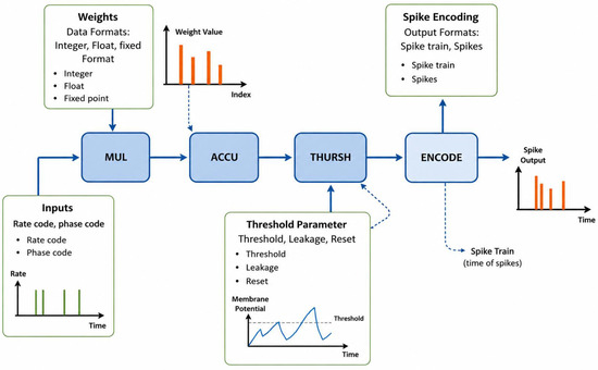
Recent advances in biologically inspired neural computation have sparked increasing interest in developing hardware-efficient architectures capable of emulating brain-like cognitive abilities like low power consumption and less inference latency. However, significant hardware overhead and spike-processing complexity remain major challenges in FPGA implementations of
[...] Read more.
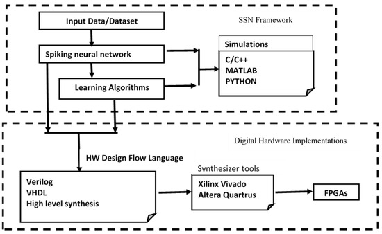
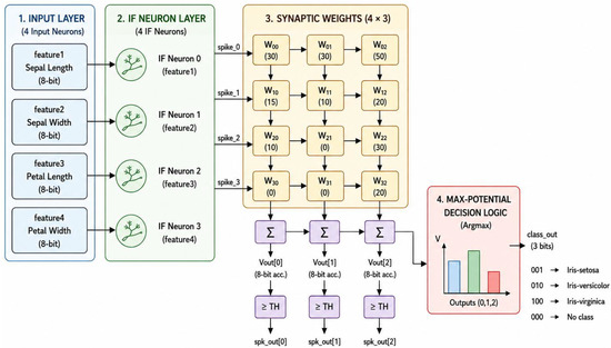
Recent advances in biologically inspired neural computation have sparked increasing interest in developing hardware-efficient architectures capable of emulating brain-like cognitive abilities like low power consumption and less inference latency. However, significant hardware overhead and spike-processing complexity remain major challenges in FPGA implementations of spiking neural networks. In this work, we propose a sparse spike-aware and weight pruning FPGA architecture based on LIF neurons that minimizes spike activity and synaptic operations through pruning-aware event-driven computation. The proposed sparse spike-aware SNN architecture was evaluated using the Iris dataset. The dataset was divided into 80% training and 20% testing samples. Pre-trained weights obtained from software-level training were deployed onto the FPGA-based LIF classifier. Classification accuracy was computed by comparing predicted output spikes against ground-truth class labels. Experimental results demonstrated that the proposed architecture achieved an overall classification accuracy of 93.3% while maintaining low hardware resource utilization and reduced power consumption. Moreover, the implementation achieves superior energy efficiency, consuming only 3.5 W total on-chip power and utilizing 587 logic cells, confirming its suitability for compact, real-time edge computing neuromorphic applications.
Full article

Graphical abstract
Open AccessArticle
Morphology–Controlled Fe/Silicone Composite Dielectric Layers via Ultrasonic Needle-Induced Acoustic Streaming for Flexible Capacitive Sensors
by
Xu Wang, Guanyu Fu, Zhiwei Xu, Yuelong Zhang, Junchao Zhang, Yinlong Zhu and Ying Liu
J. Low Power Electron. Appl. 2026, 16(3), 27; https://doi.org/10.3390/jlpea16030027 - 29 Jul 2026
Abstract
►▼
Show Figures
Achieving precise microstructure control in composite dielectric layers remains a key challenge for enhancing the sensitivity and reducing the power consumption of flexible capacitive sensors. In this work, an ultrasonic needle-induced acoustic streaming strategy is proposed to regulate the spatial distribution of Fe
[...] Read more.
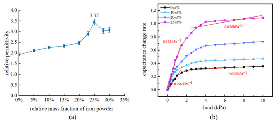
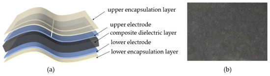
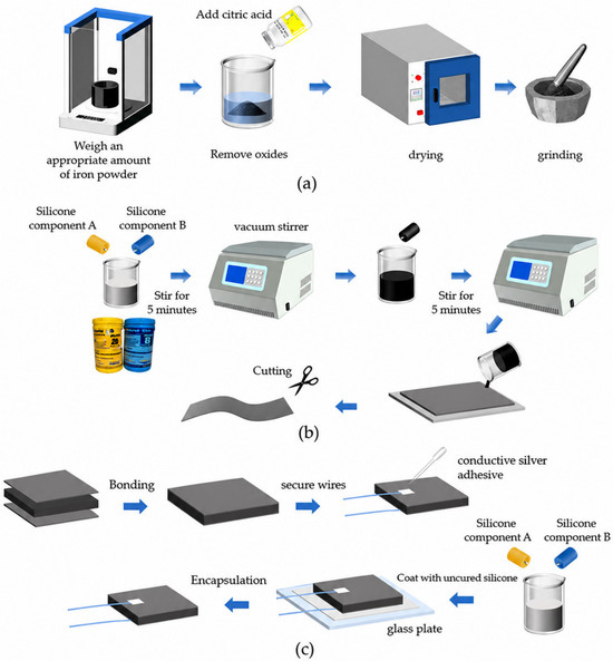
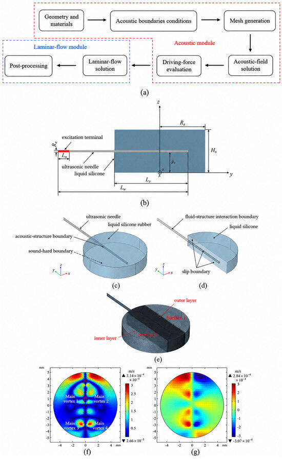
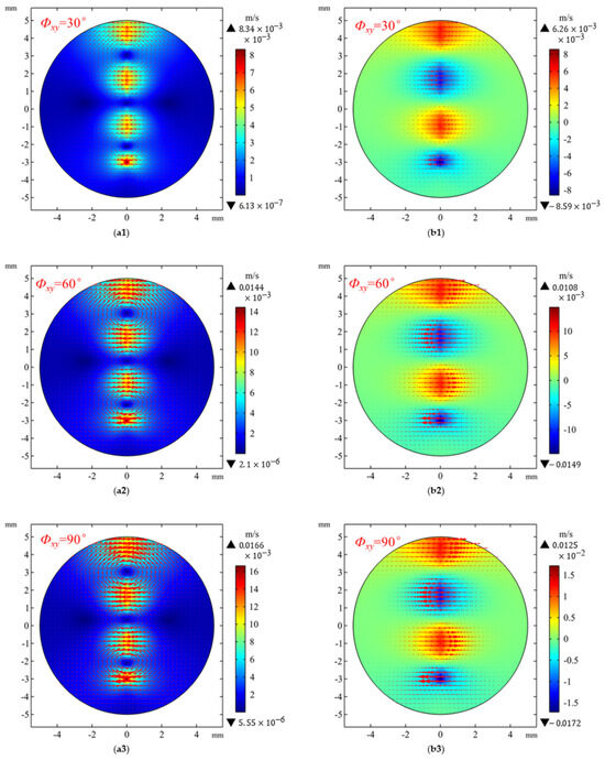
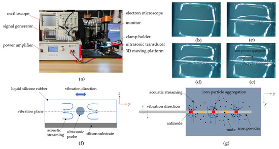
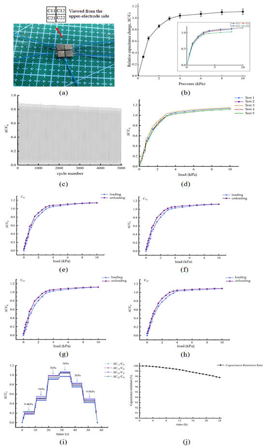
Achieving precise microstructure control in composite dielectric layers remains a key challenge for enhancing the sensitivity and reducing the power consumption of flexible capacitive sensors. In this work, an ultrasonic needle-induced acoustic streaming strategy is proposed to regulate the spatial distribution of Fe particles within a silicone matrix, enabling controllable particle migration and aggregation in liquid silicone. Multiphysics simulations reveal that, at an excitation frequency of 75.49 kHz, Fe particles are effectively driven toward the ultrasonic focal region, forming a tunable microstructure. Experimental results confirm that this method enables precise morphological control of the composite dielectric layer. The composite with 25 wt% Fe exhibits the highest measured relative permittivity of about 3.45, enabling a capacitive sensor sensitivity of 0.423 kPa−1 in the 0–1 kPa range. After acoustic-streaming optimization and integration into a four-unit capacitive array, the device achieved 0.509 kPa−1 sensitivity, retained 92.04% of its response after 5000 cycles at 3 kPa, and maintained 97.8% of its initial capacitance after 24 h. The proposed approach provides an effective route to improving sensor performance through microstructure engineering while maintaining low electrical loss. This work not only advances the design of high-performance functional composites but also expands the application of acoustic streaming techniques in low-power flexible electronics.
Full article

Figure 1
Open AccessArticle
Optimizing Chaotic Behavior: Systematic Shifting and Operations for Robust 1-D Chaotic Maps
by
Mrittika Chowdhury, Ziyi Niu, Shuai Song, Anurag Dhungel and Md Sakib Hasan
J. Low Power Electron. Appl. 2026, 16(3), 26; https://doi.org/10.3390/jlpea16030026 - 27 Jul 2026
Abstract
►▼
Show Figures
In this work, we present a systematic framework to optimize robust 1-D chaotic maps, focusing on expanding the uninterrupted chaotic region and enhancing chaotic properties throughout the entire parameter space. To achieve these objectives, we propose three distinct techniques, each involving systematic manipulations
[...] Read more.
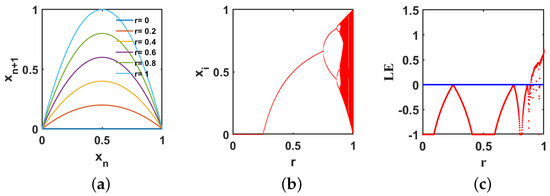
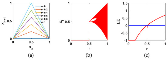
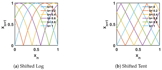
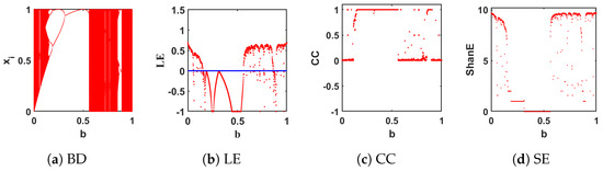
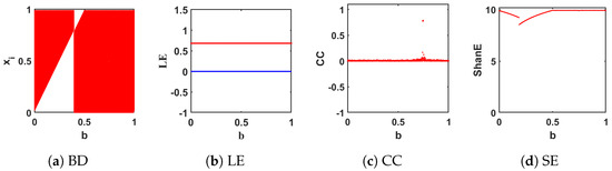
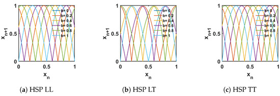
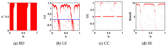
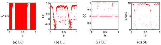
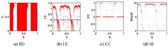
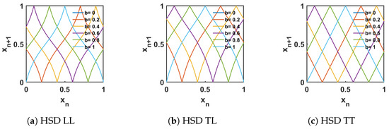
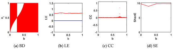
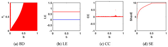
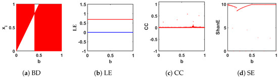
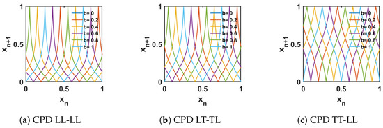
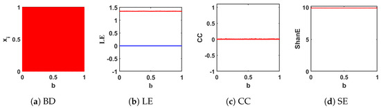
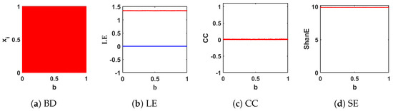
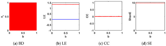
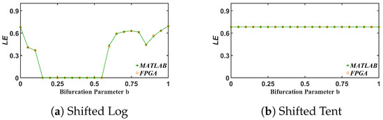
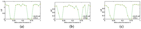
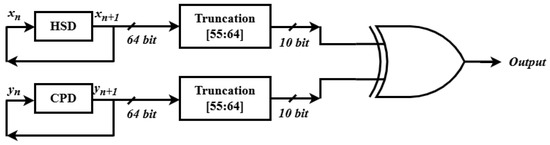
In this work, we present a systematic framework to optimize robust 1-D chaotic maps, focusing on expanding the uninterrupted chaotic region and enhancing chaotic properties throughout the entire parameter space. To achieve these objectives, we propose three distinct techniques, each involving systematic manipulations of chaotic seed maps. These manipulations include shifts and operations such as multiplication and division, which result in significant improvements in their chaotic characteristics. The effectiveness of the proposed methods is demonstrated through a comprehensive analysis using bifurcation plots, the maximum Lyapunov exponent, the correlation coefficient, Shannon entropy, the average Lyapunov exponent, and the chaotic ratio. The results illustrate the attainment of an extensive and uninterrupted chaotic range, alongside enhanced chaotic behavior due to the application of shifted maps. Additionally, in this work we also investigate the impact of combining general shifted maps with halfway-shifted maps, showing that their product leads to further improvements in chaotic properties and their division widens the chaotic ratio. In the last proposed method, the combined product division (CPD) maps achieve the highest overall performance, attaining a maximum Lyapunov exponent of 1.3567 and an average Lyapunov exponent of 1.3498, while maintaining a perfect chaotic ratio (CR = 1) across the entire parameter space. To demonstrate hardware feasibility, some of the proposed maps were also implemented on an FPGA, and the results were compared with MATLAB R2022b simulations. The close match between the two validates the practicality of implementing these chaotic systems in hardware. The proposed techniques have potential applications in areas such as random number generation, chaos-based cryptography, and secure communication, among others. To prove this, the optimized maps are leveraged to design a chaos-based pseudo-random number generator (PRNG) that passes statistical tests including NIST SP 800-22 (all 15 sub-tests passed) and TestU01 (38/38 Rabbit, 17/17 Alphabit, 102/102 BlockAlphabit), validating cryptographic-grade randomness.
Full article

Figure 1
Open AccessArticle
A Compact UWB Antenna with a Fixed WLAN Band-Notch for Low-Power Wireless Systems
by
Kaijun Song, Hanzhou Luo, Yuting Yuan and Yong Fan
J. Low Power Electron. Appl. 2026, 16(3), 25; https://doi.org/10.3390/jlpea16030025 - 12 Jul 2026
Cited by 1
Abstract
►▼
Show Figures
This paper presents a compact, ultra-wideband (UWB) antenna designed for low-power wireless systems requiring upper WLAN (5.725–5.825 GHz) interference mitigation. The antenna integrates a tapered-slot radiator for broadband impedance matching with a dual C-shaped slot resonator on the ground plane to achieve targeted
[...] Read more.
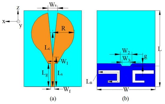
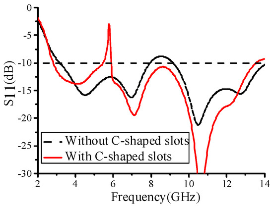
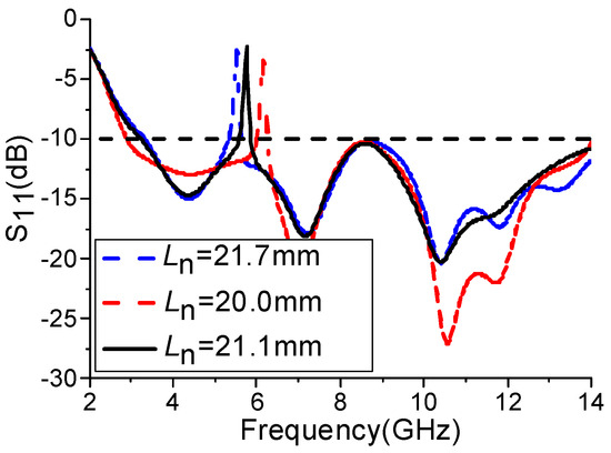
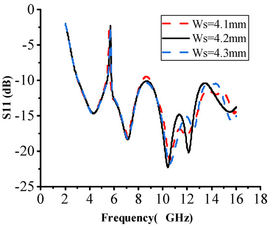
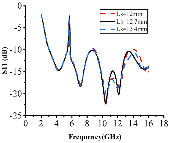
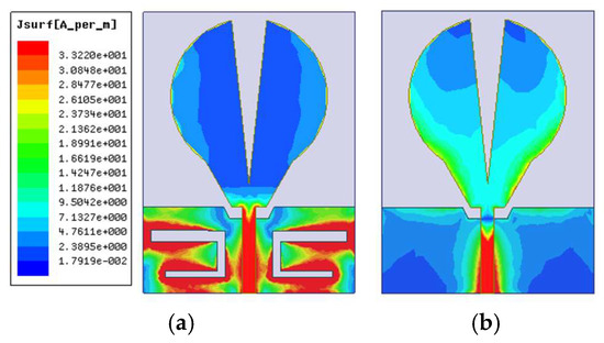
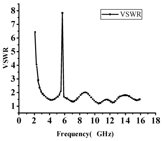
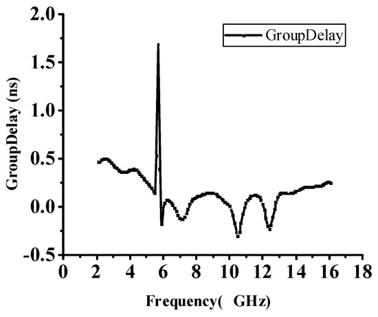
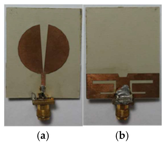
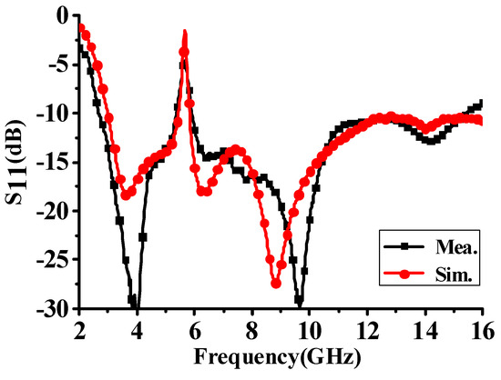
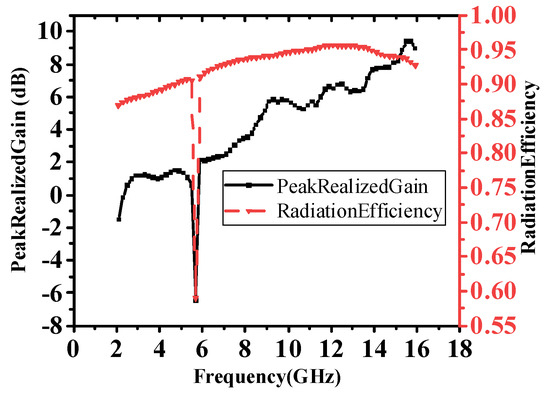
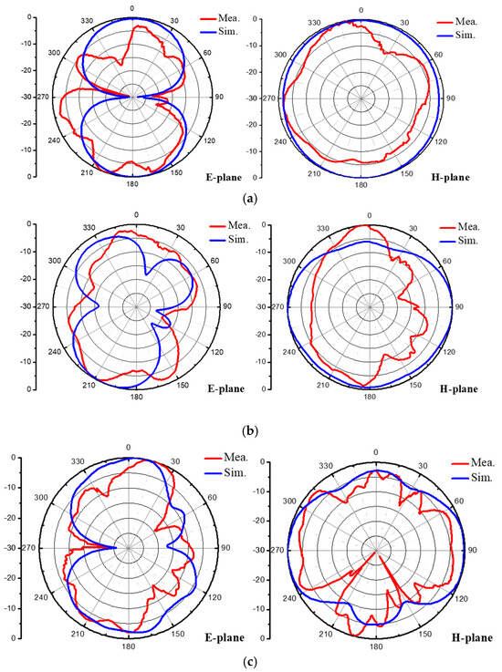
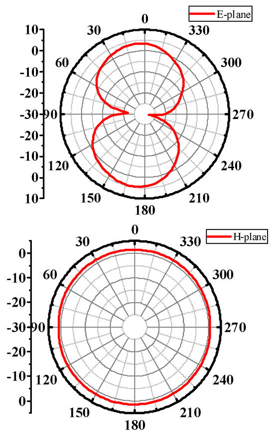
This paper presents a compact, ultra-wideband (UWB) antenna designed for low-power wireless systems requiring upper WLAN (5.725–5.825 GHz) interference mitigation. The antenna integrates a tapered-slot radiator for broadband impedance matching with a dual C-shaped slot resonator on the ground plane to achieve targeted signal rejection. By leveraging the resonant properties of the slots, interference from the WLAN band is suppressed without requiring any active components, ensuring zero additional power consumption for the filtering function. The fabricated prototype, with a compact size of 31 × 40 mm2, demonstrates an operational bandwidth from 2.68 to 16 GHz (S11 < −10 dB) with a stable peak realized gain of 2–10 dB and a radiation efficiency above 80% across the passband. At the notch center frequency of 5.72 GHz, the gain decreases by 6.4 dB and the radiation efficiency falls to 0.6, there is effective signal rejection in the target notch band, and there are stable, omnidirectional H-plane radiation patterns. The reflection coefficient at the notch frequency rises to approximately −2.2 dB, effectively suppressing radiation in the WLAN band while maintaining stable gain and omnidirectional patterns in the remaining UWB spectrum. The proposed design offers a simple, low-cost, and energy-efficient solution for achieving spectral coexistence in power-constrained UWB applications.
Full article

Figure 1
Open AccessArticle
Can Federated Learning Go Green? EcoFL: A System-Level Energy-Aware Benchmark for IoT Edge Intelligence
by
Tymoteusz Miller and Irmina Durlik
J. Low Power Electron. Appl. 2026, 16(3), 24; https://doi.org/10.3390/jlpea16030024 - 8 Jul 2026
Abstract
The proliferation of Internet of Things (IoT) devices operating at the network edge has created unprecedented demand for distributed machine learning capable of functioning under severe resource constraints. Federated learning (FL) has emerged as a promising paradigm for privacy-preserving collaborative model training across
[...] Read more.
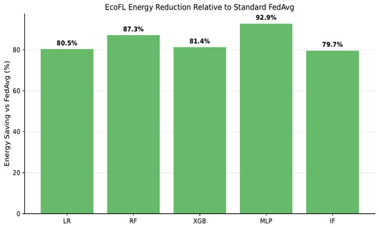
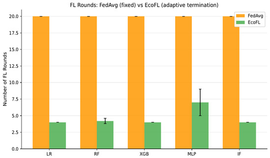
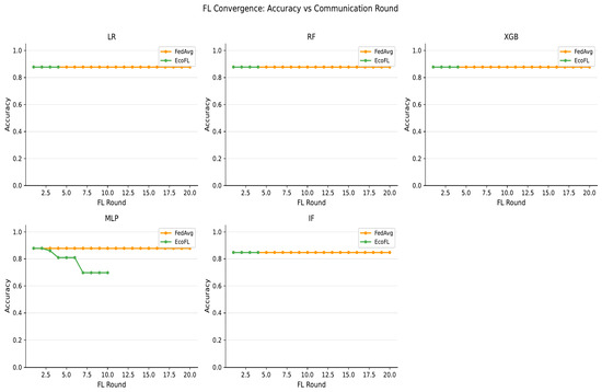
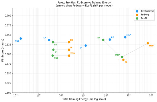
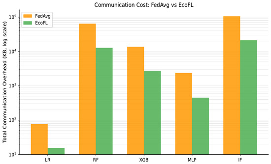
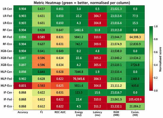
The proliferation of Internet of Things (IoT) devices operating at the network edge has created unprecedented demand for distributed machine learning capable of functioning under severe resource constraints. Federated learning (FL) has emerged as a promising paradigm for privacy-preserving collaborative model training across distributed nodes; however, its application to energy-constrained edge environments remains insufficiently characterized at the system level, particularly with respect to reproducible evaluation of resource consumption and communication efficiency. In this paper, we present EcoFL (Energy-Conscious Federated Learning), a modular, energy-aware benchmarking and orchestration framework for systematic evaluation of lightweight machine learning models under emulated edge hardware constraints. Rather than proposing a new federated optimization algorithm, EcoFL extends a standard FedAvg-based training pipeline with three principal components: (i) an energy-aware communication scheduler that dynamically adapts aggregation rounds and client participation based on per-node resource availability; (ii) a comprehensive system-level profiling pipeline capturing CPU utilization, RAM consumption, inference latency, communication overhead, and estimated computational energy consumption per training round; and (iii) a reproducible benchmarking methodology enabling fair comparison of centralized, standard federated (FedAvg), and energy-aware federated configurations. We evaluate five lightweight model families—Logistic Regression, Random Forest, XGBoost, Multilayer Perceptron, and Isolation Forest—under emulated Raspberry Pi 4 hardware constraints using an anomaly detection task on synthetic IoT sensor telemetry (50,000 samples, 12 features, Dirichlet non-IID partitioning). Experimental results across five independent seeds show that, within the evaluated benchmark setting, EcoFL reduces estimated federated training energy by 79.9–92.9% (mean 84.4%) relative to standard FedAvg through adaptive round termination (4–7 rounds versus 20 fixed rounds), while showing no statistically significant F1-score degradation for four of the five evaluated model families under the tested seed regime. Notably, EcoFL achieves a higher F1-score than FedAvg for Random Forest (+0.052), which we attribute to reduced overfitting resulting from earlier convergence under non-IID data distributions. The full EcoFL framework is released as open-source software to promote reproducibility in energy-aware federated learning research and to facilitate systematic investigation of the trade-offs between predictive performance, resource utilization, and communication overhead in resource-constrained edge environments.
Full article
(This article belongs to the Special Issue 15th Anniversary of Journal of Low Power Electronics and Applications)
►▼
Show Figures

Figure 1
Open AccessArticle
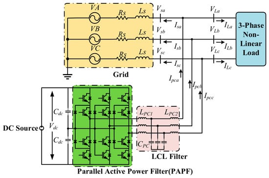
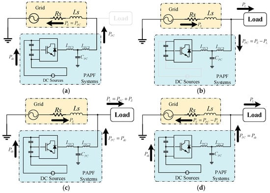
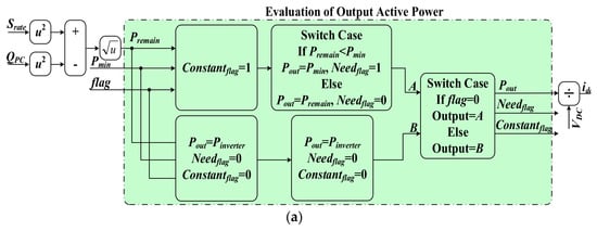
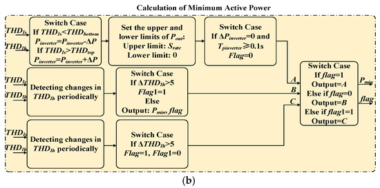
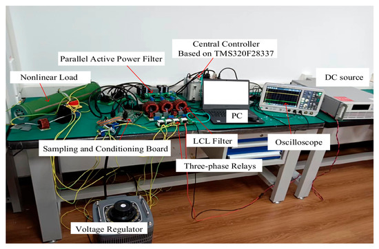
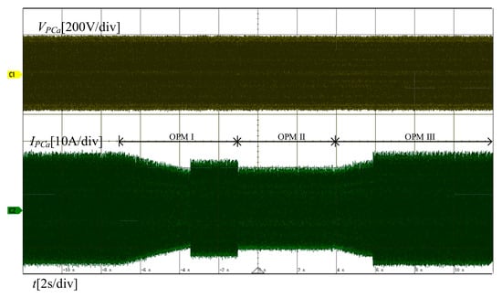
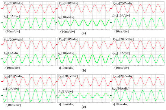
An Automated Capacity-Allocating-Based Transition Strategy Between Harmonic and Reactive Power Compensation for Multifunctional PAPF
by
Tao Zhang, Yao Zhang, Yufeng Zhang, Zhonghua Yao and Yunhong Shao
J. Low Power Electron. Appl. 2026, 16(3), 23; https://doi.org/10.3390/jlpea16030023 - 6 Jul 2026
Abstract
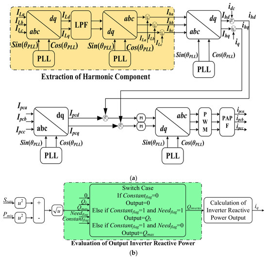
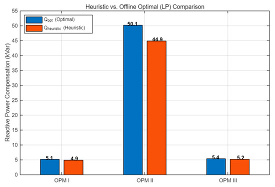
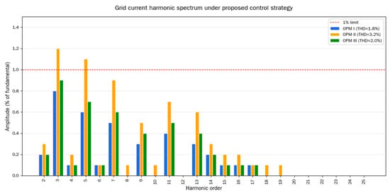
This paper proposes a practical heuristic engineering strategy for automated capacity allocation in a multifunctional parallel active power filter (PAPF) that simultaneously provides harmonic and reactive power compensation. Unlike theoretically optimal methods, our approach prioritizes real-time feasibility and ease of implementation. The key
[...] Read more.
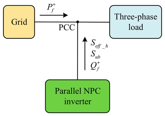
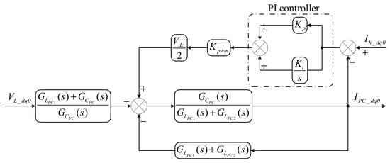
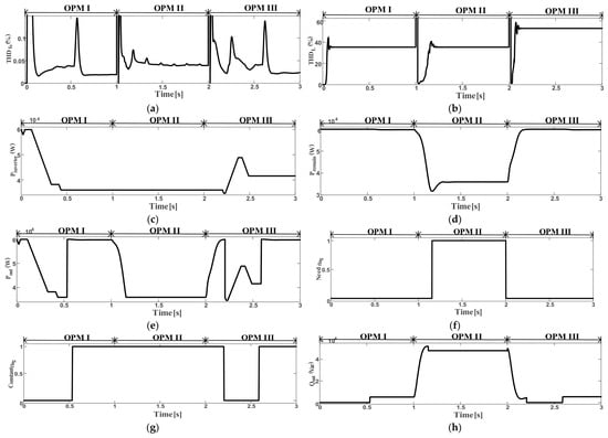
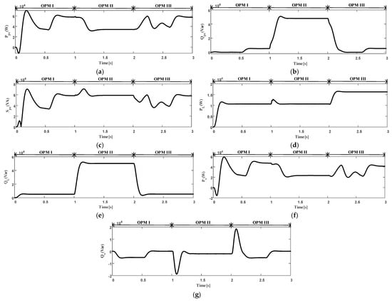
This paper proposes a practical heuristic engineering strategy for automated capacity allocation in a multifunctional parallel active power filter (PAPF) that simultaneously provides harmonic and reactive power compensation. Unlike theoretically optimal methods, our approach prioritizes real-time feasibility and ease of implementation. The key features are: (1) an event-triggered, closed-loop THD-feedback mechanism that dynamically recalculates the minimum active power required for harmonic compensation only when the load harmonic content changes, avoiding periodic computational waste; (2) a strict priority handling that guarantees grid current THD below 5% (IEEE-519 compliant) under all operating conditions, even when capacity is severely insufficient; (3) a closed-loop transition mechanism that uses measured grid current THD and remaining capacity as feedback inputs to continuously adapt power distribution. The proposed rule-based strategy does not claim theoretical optimality but provides a verifiable, ready-to-implement solution with experimental evidence. Simulation and experimental results on a three-level NPC PAPF prototype demonstrate that the strategy maintains grid current THD below 5% while keeping the apparent power within the rated capacity, achieving near-optimal reactive compensation (92–96% of the optimum) without iterative optimization. The experimental validation includes efficiency measurements, switching-loss estimation, DSP timing analysis, and robustness tests under grid disturbances. Future work will extend the concept to multi-inverter systems using multi-objective optimization and AI-based allocation.
Full article
(This article belongs to the Special Issue Energy Consumption Management in Electronic Systems)
►▼
Show Figures

Figure 1

Open AccessArticle
A Low-Power Mixed-Signal Differential In-Memory Matrix–Vector Computing Circuit Architecture with RISC-V Control for Edge AI
by
David Ng, King Hang Lam, Si Qi Bu, Wen Chin Lo, Chi Hong Chan, Roy Ng, Sunny Chan, Matt Mak, Hugo Wong, Steve Chim, Patrick Chang, Raymond Chik, Steven Wong and Wai Ming To
J. Low Power Electron. Appl. 2026, 16(3), 22; https://doi.org/10.3390/jlpea16030022 - 24 Jun 2026
Abstract
Analog in-memory computing (AIMC) has emerged as a promising approach to mitigate the Von Neumann bottleneck in matrix operations, which are common in deep learning applications. However, the practical implementation of resistive crossbar arrays is limited by challenges in signed weight representation, conductance
[...] Read more.
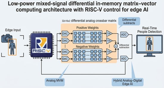
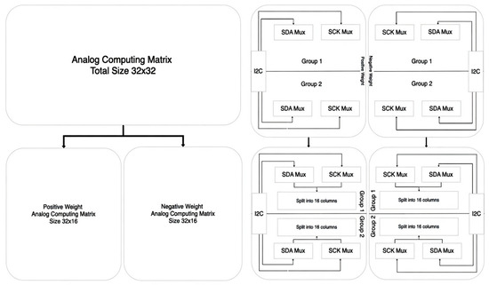
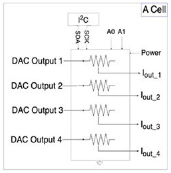
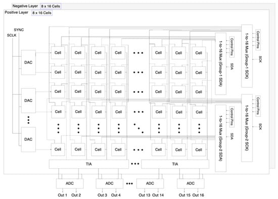
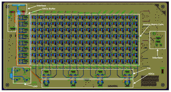
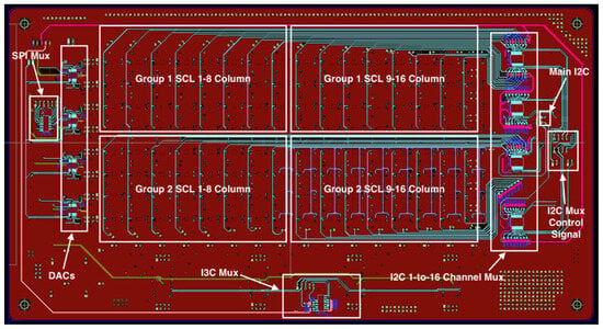
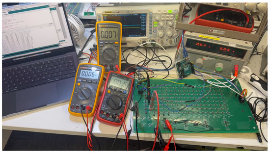
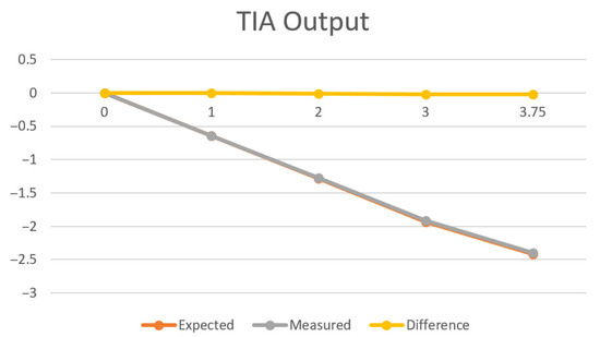
Analog in-memory computing (AIMC) has emerged as a promising approach to mitigate the Von Neumann bottleneck in matrix operations, which are common in deep learning applications. However, the practical implementation of resistive crossbar arrays is limited by challenges in signed weight representation, conductance quantization, and device nonlinearity. This paper presents a differential mixed-signal architecture for accurate signed matrix–vector multiplication (MVM), integrated with a RISC-V microcontroller for edge inference applications. A structured digital-to-analog mapping framework encodes quantized neural network weights into programmable conductance values while preserving arithmetic correctness. The design employs voltage-mode input encoding, differential current summation, and transimpedance-based readout followed by analog-to-digital conversion, enabling single-cycle signed accumulation without duplicating crossbar resources. A 32 × 16 dual-layer prototype crossbar was fabricated and experimentally characterized. Measurements demonstrate a mean absolute percentage error (MAPE) below 1% within the linear operating region and below 4% over the full-scale conductance range. These results validate the robustness of the proposed mapping methodology and confirm the feasibility of hybrid analog–digital acceleration for edge AI systems. Consequently, this discrete prototype serves as a physical verification platform for the AIMC approach, providing valuable insights for more efficient mixed-signal computing integrated circuit (IC) designs.
Full article
(This article belongs to the Topic Advanced Integrated Circuit Design and Application)
►▼
Show Figures

Graphical abstract
Open AccessReview
3D Integrated DNN Accelerators: Recent Trends and Future Prospects
by
Abrar Abdurrob, Aristotelis Tsekouras, Evangelos Tzouvaras, Vasilis F. Pavlidis and Emre Salman
J. Low Power Electron. Appl. 2026, 16(2), 21; https://doi.org/10.3390/jlpea16020021 - 18 Jun 2026
Abstract
The rapid growth of Deep Neural Networks (DNNs) has led to the development of application-specific DNN accelerators. Conventional 2D von Neumann architectures suffer from memory bandwidth limitations between the memory and the processing core. 3D DNN accelerators have emerged as a promising solution
[...] Read more.
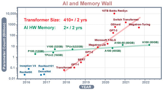
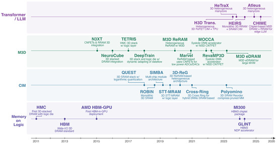
The rapid growth of Deep Neural Networks (DNNs) has led to the development of application-specific DNN accelerators. Conventional 2D von Neumann architectures suffer from memory bandwidth limitations between the memory and the processing core. 3D DNN accelerators have emerged as a promising solution by leveraging 3D integration to enable near-memory logic or in-memory computation. By shifting computation closer to memory, these accelerators significantly reduce data movement and therefore latency, resulting in more energy-efficient operations. Monolithic 3D (M3D) integration, in particular, enables high-bandwidth systems by utilizing high-density monolithic inter-tier vias (MIVs). This paper provides a critical review of recent advances in 3D DNN accelerators that combine near-memory and compute-in-memory with various 3D technologies, offering a useful discussion and future prospects of the available technologies and architectures that have advanced the performance of DNN accelerators. Particular attention is devoted to accelerators for emerging transformer-based large language model (LLM) networks due to the higher memory demands. Thermal-aware design techniques of 3D DNN accelerators are also discussed as a means to address the fundamental challenge of heat dissipation. A detailed review is finally conducted on package-level constraints, considering signal integrity, power delivery, and thermo-mechanical reliability.
Full article
(This article belongs to the Special Issue 15th Anniversary of Journal of Low Power Electronics and Applications)
►▼
Show Figures

Figure 1

Open AccessReview
Wearable, Self-Powered Electronic Devices: Logical Framework for Transforming the Future of Digital Health
by
Jegan Rajendran, Nimi Wilson Sukumari and Manikandan Rajendran
J. Low Power Electron. Appl. 2026, 16(2), 20; https://doi.org/10.3390/jlpea16020020 - 16 Jun 2026
Cited by 1
Abstract
►▼
Show Figures
The increasing demand of digital technologies and their integration with wearable health devices provides an efficient trigger for next-generation wearable healthcare devices for long-term physiological monitoring. The advancement of energy harvesting mechanism, nanomaterial-based sensor fabrication and their integration with digital technologies have emerged
[...] Read more.
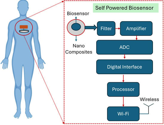
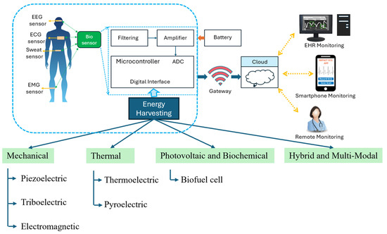
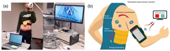
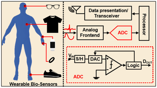
The increasing demand of digital technologies and their integration with wearable health devices provides an efficient trigger for next-generation wearable healthcare devices for long-term physiological monitoring. The advancement of energy harvesting mechanism, nanomaterial-based sensor fabrication and their integration with digital technologies have emerged as a promising solution for transforming future of digital health. This study provides a comprehensive summary and framework for wearable self-powered electronic devices, enabling continuous, battery-free health monitoring and advancing the development of sustainable, next-generation digital healthcare systems. This review paper presents a broad and detailed overview of current technologies and sensors advancement in developing low-power wearable, self-powered electronic devices suitable for healthcare applications. The importance and reliable use of key energy harvesting approaches including triboelectric, piezoelectric, thermoelectric, and photovoltaic approaches are systematically presented which focused on development of energy efficient wearable devices. This review further examines the low-power circuit design strategies for flexible electronics focusing personalized healthcare monitoring. Current challenges and limitations related to advanced manufacturing of wearable health devices focusing on large-scale deployment are also analyzed. Finally, the key future research directions are outlined for advancing a next-generation intelligent digital health system.
Full article

Graphical abstract
Open AccessFeature PaperArticle
Design of an X-Band CMOS VCO with a Transformer-Coupled and Transconductance-Boosted Stacked Topology
by
Yen-Ying Peng, Syu-Bin Li, Sen Wang and Chatrpol Pakasiri
J. Low Power Electron. Appl. 2026, 16(2), 19; https://doi.org/10.3390/jlpea16020019 - 15 Jun 2026
Abstract
This paper presents the design and implementation of an X-band voltage-controlled oscillator (VCO) fabricated in a standard 180-nm CMOS process. To sustain stable oscillation under a constrained power budget, a gm-boosted topology is employed, integrating vertically stacked cross-coupled transistors with a center-tapped
[...] Read more.
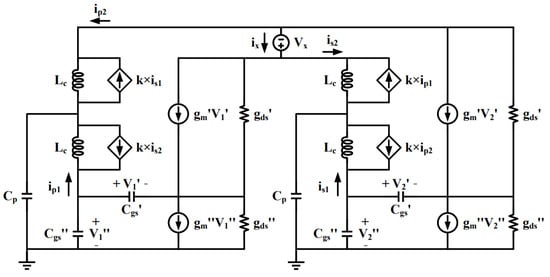
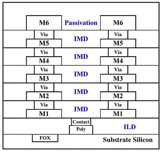
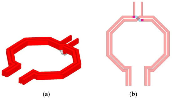
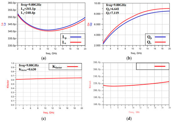
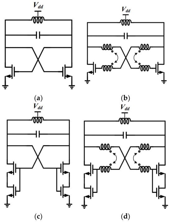
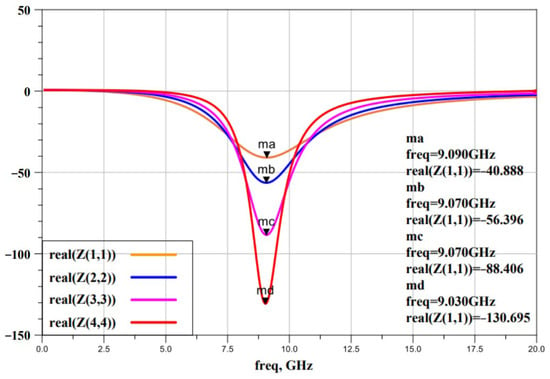
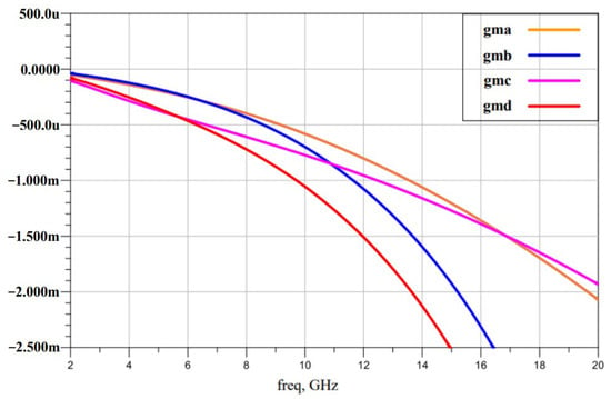
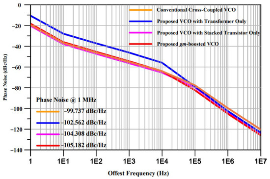
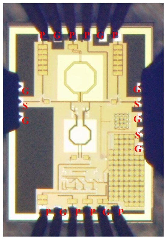
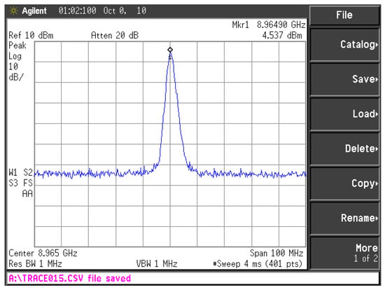
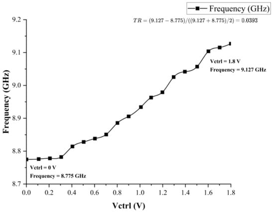
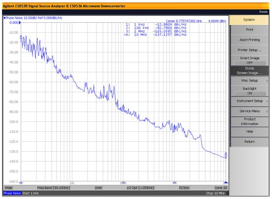
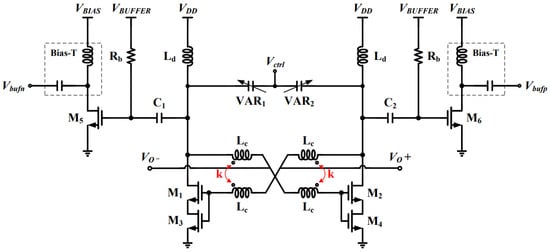
This paper presents the design and implementation of an X-band voltage-controlled oscillator (VCO) fabricated in a standard 180-nm CMOS process. To sustain stable oscillation under a constrained power budget, a gm-boosted topology is employed, integrating vertically stacked cross-coupled transistors with a center-tapped transformer to enhance the equivalent negative conductance. The boosting is achieved through two complementary mechanisms: the center-tapped transformer performs an impedance transformation that repurposes the layout parasitic capacitances into transconductance-enhancing elements, while the stacked cross-coupled pair reuses the DC current and suppresses the source-degeneration of a conventional pair, jointly sustaining a robust start-up margin at a low 0.75 V supply. On-wafer measurement results demonstrate a frequency tuning range from 8.78 GHz to 9.13 GHz as the control voltage is swept from 0 V to 1.8 V, with an average VCO gain KVCO of 447.5 MHz/V. Under a total DC power consumption of 6.9 mW, the oscillator delivers an output power of 4.54 dBm and exhibits a measured phase noise of −103 dBc/Hz at a 1-MHz offset.
Full article
(This article belongs to the Topic Advanced Integrated Circuit Design and Application)
►▼
Show Figures

Figure 1
Open AccessArticle
Thermal Nonuniformity-Aware Reliability Screening for Systolic AI Accelerators
by
Larisa Goffman-Vinopal
J. Low Power Electron. Appl. 2026, 16(2), 18; https://doi.org/10.3390/jlpea16020018 - 31 May 2026
Abstract
AI accelerators increasingly operate under tight power, thermal, voltage, and timing margins, making workload-dependent thermal nonuniformity an important reliability concern. In systolic AI accelerators, localized activity concentration can create spatially uneven thermal stress, but thermal or timing-exposure analysis alone does not determine whether
[...] Read more.
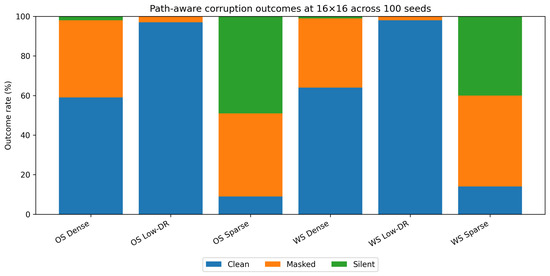
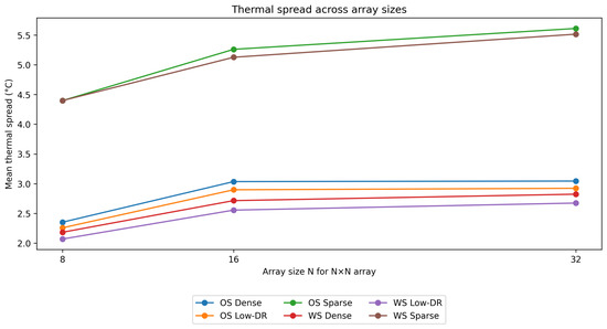
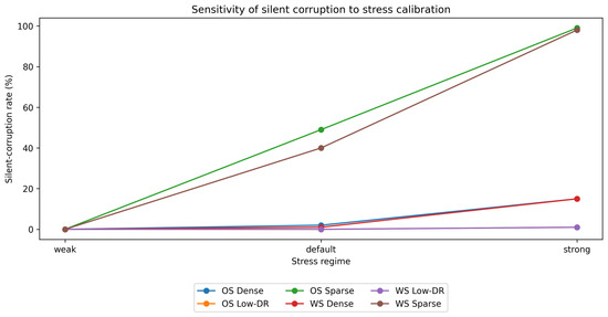
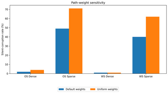
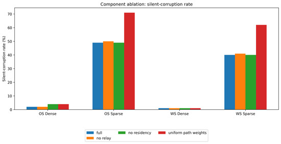
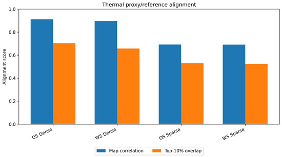
AI accelerators increasingly operate under tight power, thermal, voltage, and timing margins, making workload-dependent thermal nonuniformity an important reliability concern. In systolic AI accelerators, localized activity concentration can create spatially uneven thermal stress, but thermal or timing-exposure analysis alone does not determine whether such stress remains benign, becomes numerically masked, or propagates into silent corruption. This paper presents a cross-layer early-stage screening methodology for thermal nonuniformity-aware reliability analysis in systolic arrays. The framework links workload-aware activity extraction, relative power concentration modeling, diffusion-based thermal proxy analysis, an explicit thermal-to-timing stress abstraction, path class-aware corruption modeling, and clean/masked/silent outcome classification. The revised framework is formalized mathematically and evaluated across dense, low-dynamic-range, and sparse GEMM workloads under weight-stationary and output-stationary execution. To strengthen statistical and methodological confidence, the study includes 100-seed corruption reruns with Wilson confidence intervals, thermal scaling across , , and arrays, calibration sensitivity, path weight sensitivity, component ablations, and preliminary compact thermal reference alignment. The results show that sparse workloads consistently produce the largest thermal spread across tested array sizes, while dense and low-dynamic-range workloads remain more spatially uniform. Under the default calibrated screening regime at , sparse output-stationary and sparse weight-stationary cases reach 49% and 40% silent corruption rates, respectively, while dense cases remain mostly clean or masked and low-dynamic-range cases remain largely clean. Sensitivity and ablation experiments show that the sparse workload risk is not caused by one isolated modeling component, although the masked/silent split depends on path class weighting and thermal diffusion assumptions. The main contribution is not signoff-accurate silicon failure prediction, but a reproducible screening front end for identifying workload, dataflow, and path class combinations that deserve deeper thermal, timing, RTL-level, and application-level validation.
Full article
(This article belongs to the Topic Advanced Integrated Circuit Design and Application)
►▼
Show Figures

Figure 1

Open AccessArticle
A Low-Power 68.4 dB Signal-to-Noise-and-Distortion Ratio Noise-Shaping SAR ADC for Biomedical Applications
by
Thi Phuong Ha, The Khai Chu, Van Tung Nguyen, Orazio Aiello and Xuan Thanh Pham
J. Low Power Electron. Appl. 2026, 16(2), 17; https://doi.org/10.3390/jlpea16020017 - 7 May 2026
Abstract
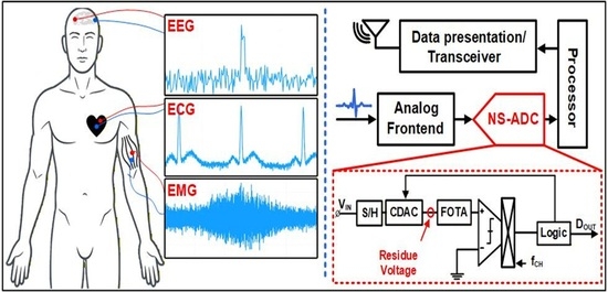
This paper introduces a novel analog-to-digital converter (ADC) employing a passive noise-shaping (NS) technique combined with a chopper-stabilized comparator, enhancing performance and reducing ripple factor while maintaining low power consumption. The NS architecture is built on a cascade-integrator feedforward (CIFF) structure, using both
[...] Read more.
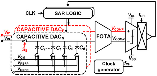
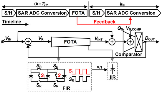
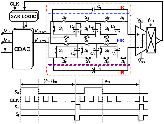
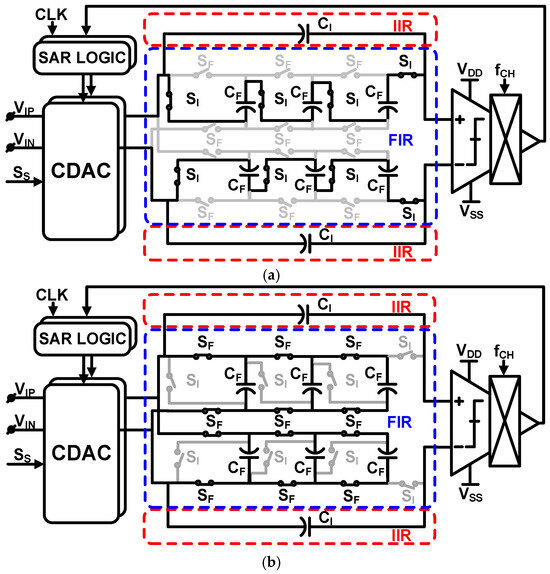
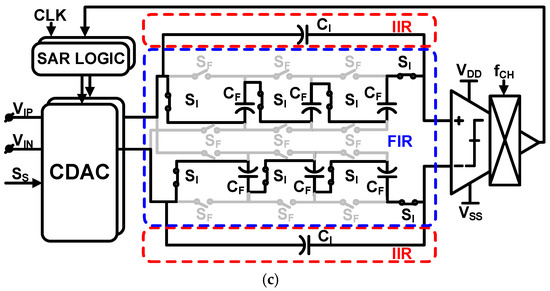
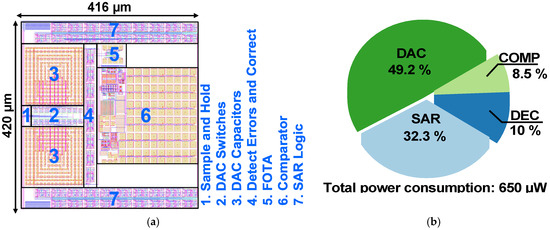
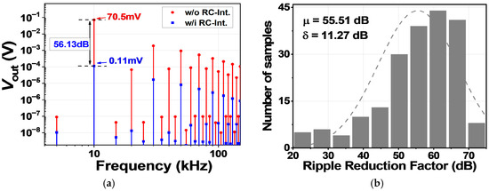
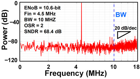
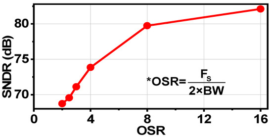
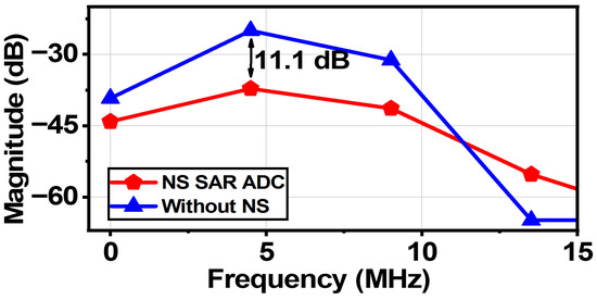
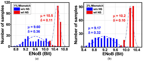
This paper introduces a novel analog-to-digital converter (ADC) employing a passive noise-shaping (NS) technique combined with a chopper-stabilized comparator, enhancing performance and reducing ripple factor while maintaining low power consumption. The NS architecture is built on a cascade-integrator feedforward (CIFF) structure, using both infinite- and finite-impulse response filters to minimize quantization and kT/C noise. Additionally, it employs a low-power two-stage chopper amplifier to compensate for the offset voltage and enhance system stability. Validated according to the 180 nm CMOS process, the proposed ADC has an effective number of bits of 10.6, a signal-to-noise-and-distortion ratio of 68.4 dB, and a signal-to-noise ratio of 59.33 dB. With a compact area of 0.17 mm2 and a power consumption of 650 µW from a 1.8 V supply, the proposal is well suited to biomedical sensor applications requiring strict accuracy and low energy consumption.
Full article
(This article belongs to the Special Issue Ultra-Low-Power ICs for the Internet of Things (3rd Edition))
►▼
Show Figures

Graphical abstract
Highly Accessed Articles
Latest Books
E-Mail Alert
News
1 September 2026
MDPI INSIGHTS: The CEO’s Letter #38 – 2 Million Published Articles, Outstanding Reviewers, Michele Parrinello Award, AIS 2026 & WSF-12
Topics
Topic in
Electronics, Eng, JLPEA, Micromachines, Nanomaterials
Advanced Integrated Circuit Design and Application
Topic Editors: Shoue Chen, Xiaolong Wang, Ke XieDeadline: 25 December 2026
Topic in
Applied Sciences, Electronics, Energies, Sensors, Chips, JLPEA
VLSI-Based Sequential Devices in Cyber-Physical Systems
Topic Editors: Alexander Barkalov, Larysa Titarenko, Kazimierz KrzywickiDeadline: 30 April 2027
Topic in
Electricity, Electronics, JLPEA, Processes, Applied Sciences, Sustainability, Sci
Advances in Power Electronics and Energy Conversion Systems: Multi-Domain Integration, Optimization, and Resilience for Next-Generation Energy Infrastructure
Topic Editors: Hongjian Lin, Dong Xie, Xiangyu Meng, Junyu Chen, Weiyu WangDeadline: 31 May 2027
Topic in
Electronics, Materials, Nanomaterials, Sensors, Biosensors, JLPEA
Intelligent Sensing Materials and Devices
Topic Editors: Chao Cai, Zhe ChenDeadline: 30 April 2028
Special Issues
Special Issue in
JLPEA
Sustainable Wireless Sensor Networks: Recent Trends and Advances
Guest Editors: Dionisis Kandris, Eleftherios AnastasiadisDeadline: 30 September 2026
Special Issue in
JLPEA
15th Anniversary of Journal of Low Power Electronics and ApplicationsGuest Editor: Davide BertozziDeadline: 30 September 2026
Special Issue in
JLPEA
Energy Consumption Management in Electronic Systems
Guest Editors: Spyridon Nikolaidis, Ronald TetzlaffDeadline: 30 October 2026
Special Issue in
JLPEA
Ultra-Low-Power ICs for the Internet of Things (3rd Edition)
Guest Editor: Orazio AielloDeadline: 31 October 2026