Skip to Content

Journal of Low Power Electronics and Applications

Journal of Low Power Electronics and Applications is an international, peer-reviewed, open access journal on low power electronics published quarterly online by MDPI.   

Get Alerted

Add your email address to receive forthcoming issues of this journal.

All Articles (613)

  • Article
  • Open Access

This article proposes a new integrated analog implementation of the Pan–Tompkins algorithm. This algorithm, generally implemented in the digital domain at the cost of higher power consumption, is one of the most efficient for QRS detection in electrocardiographic signals. This circuit has been designed for use on small mammals like rats for the study of pulmonary arterial hypertension. The specificities of the architecture proposed in this article are a sub-threshold-operated architecture to perform the amplification, noise filtering, and differentiation of the signal in a unique block to limit the power consumption; an analog squarer; and an analog monostable reshaping-circuit followed by a digital counter clocked by an ultra-low power relaxation oscillator. Compared with the state of the art, this circuit, designed with the X-FAB xh018 180 nm CMOS technology, presents one of the lowest power consumptions currently reported, at 28.5 nW, 76% of which is consumed in the current, voltage, and time references. Post-layout simulation results show a reliable 98.57% heart beat detection accuracy using the MIT-BIH arrhythmia database and 99.85% accuracy for healthy sinus rhythm electrocardiograms. The robustness of the circuit is also investigated, and mitigating solutions are proposed for each critical block.

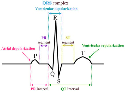
Typical aspect of an ECG signal for mammals.
  • Article
  • Open Access

Reliable Cu/polyimide (PI) metallization requires strong interfacial adhesion while minimizing the thickness of the metallic adhesion layer. In this study, Ni ion implantation was combined with physical vapor deposition to construct an ultrathin Ni interlayer on a 25 μm-thick PI substrate. Three metallization schemes were compared: 20 nm Ni/2 μm Cu, 10 nm Ni/2 μm Cu, and Ni-ion-implanted PI/5 nm Ni/2 μm Cu. Ni ions were implanted at an energy of 5 keV and a fluence of 1 × 10¹⁴ ions cm−2. The implantation treatment decreased the water contact angle of PI from 75° to 64° and increased its surface free energy from 36.41 to 42.99 mJ m−2, primarily through an increase in the polar component. Surface observations showed uniformly distributed implantation-associated micro/nanostructures with characteristic dimensions of approximately 50–300 nm, which may provide additional nucleation and anchoring sites for the subsequently deposited Ni layer. Cross-sectional transmission electron microscopy showed an undulating, locally embedded Ni/PI interface, while elemental profiles were consistent with a gradual transition across the modified interfacial region. The Ni-ion-implanted sample with a 5 nm Ni interlayer exhibited an average 180° peel strength of 1.13 N mm−1, compared with 0.62 and 0.30 N mm−1 for the 20 and 10 nm Ni interlayers, respectively. It also showed the lowest measured sheet resistance of 3.25 mΩ sq−1. Taken together, these results suggest that, under the conditions examined, Ni ion implantation can support a reduction in deposited Ni thickness while maintaining or improving the adhesion and electrical performance of Cu/PI metallization.

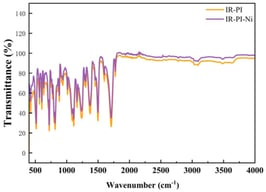
ATR-FTIR spectra of pristine PI (IR-PI) and PI after Ni-ion implantation at 5 keV and 1 × 10¹⁴ ions cm−2 (IR-PI-Ni).
  • Article
  • Open Access

This paper presents a wideband circularly polarized (CP) stacked patch antenna for 5G Sub-6 GHz applications. A major challenge in wideband dual-feed antennas is the fabrication limit caused by standard chemical etching and mechanical milling processes for extremely narrow high-impedance microstrip lines in two-stage branch-line couplers. To overcome this bottleneck, a Defected Ground Structure (DGS) is utilized. By etching the ground plane, the distributed inductance is increased, allowing the highly sensitive narrow traces to be physically widened while strictly maintaining the 50 Ω impedance. The antenna features an aperture-coupled mechanism via an H-shaped slot to excite the driven and parasitic patches, which are separated by an air gap to maximize bandwidth. The fabricated prototype demonstrates an impedance bandwidth ( ) of 41.6% (2.92–4.37 GHz) and a simulated 3 dB axial ratio bandwidth of 23.14% (3.26–4.07 GHz) with a peak realized gain of 7.54 dBi. Excellent agreement between simulated and measured results validates the robustness of the proposed DGS technique against fabrication tolerances.

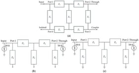
Equivalent circuit models of the proposed DGS-enhanced two-stage branch-line coupler: (a) full four-port schematic, (b) even-mode half-circuit with open-ended stubs, and (c) odd-mode half-circuit with short-ended stubs.
  • Article
  • Open Access

Massive Multiple-Input Multiple-Output (MIMO) is a key enabling technology for fifth-generation (5G) and beyond wireless communication systems because of its ability to greatly enhance both spectral efficiency (SE) and energy efficiency (EE). However, maximizing these two performance metrics simultaneously remains a challenging multi-objective optimization problem due to the conflicting effects of the transmit power, antenna deployment, and circuit power consumption. This paper investigates the EE–SE trade-off in a downlink Massive MIMO system with Minimum Mean Square Error (MMSE) channel estimation (CE) and different linear combining and precoding techniques. A power optimization framework based on transmit power allocation and antenna configuration is analyzed to identify operating points that maximize EE while maintaining high SE. Performance analysis of the number of base station (BS) antennas in MIMO systems, user equipment density, transmit power, and inter-cell interference on system performance is evaluated through numerical simulations. The results demonstrate that appropriately selecting the number of transmit antennas and optimizing the transmit power significantly improve the EE–SE trade-off. Furthermore, although increasing the number of antennas enhances SE, EE exhibits a non-monotonic behavior because of the additional circuit power required by the radio-frequency hardware. The findings confirm that MMSE-based CE provides higher spectral efficiency than the MR, ZF, RZF, and S-MMSE schemes, albeit at increased computational complexity, offering useful design guidelines for energy-efficient Massive MIMO networks.

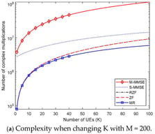
When employing various combining strategies, the number of complex multiplications per coherence block.

Featured Articles of Last Quarter

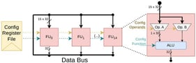
Original Versat’s data engine structure: 15 functional units (FU0–FU14) share a data bus (black) and are each configured by the Config Register File along the operand-select path (gold, dashed) and the function-select path (teal, dashed); “
  
    (
    …
    )
  
” marks the elided units FU2–FU13. The right-hand detail shows a single unit: two operand multiplexers (Op. A, Op. B) feeding an ALU.
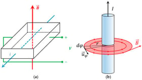
(a) Hall effect principle: a current i flowing through a conductor exposed to a perpendicular magnetic field 


        B
      
      →
    
  
 results in an electric field perpendicular to both magnitudes, creating a measurable potential V proportional to the magnetic field strength. (b) Magnetic field generated by a single current I circulating along a wire: contactless Hall detection of 
  
    B
  
 transduces the current I.

Highly Accessed Articles

News & Conferences

Latest Issues

Open for Submission

Journal Sections

XFacebookLinkedIn
J. Low Power Electron. Appl. - ISSN 2079-9268