by
Elisabetta Moisello 1,* , Maria Eloisa Castagna 2, Antonella La Malfa 2, Giuseppe Bruno 2, Piero Malcovati 1 and Edoardo Bonizzoni 1
, Maria Eloisa Castagna 2, Antonella La Malfa 2, Giuseppe Bruno 2, Piero Malcovati 1 and Edoardo Bonizzoni 1
1
Department of Electrical, Computer and Biomedical Engineering, University of Pavia, Via Ferrata 5, 2100 Pavia, Italy
2
STMicroelectronics, 95121 Catania, Italy
Micromachines 2022, 13(6), 934; https://doi.org/10.3390/mi13060934 - 11 Jun 2022
Cited by 1 | Viewed by 3099
Abstract
This paper presents a detailed analysis of a micromachined thermopile detector featuring high responsivity and a versatile mosaic structure, based on 128 60 µm × 60 µm pixels connected in series and/or in parallel. The mosaic structure is based on the one employed
[...] Read more.
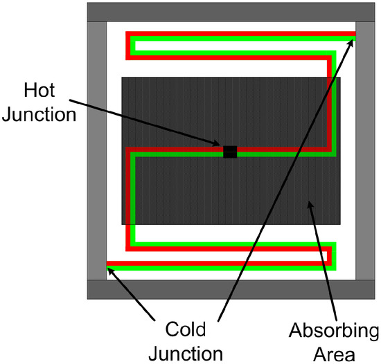
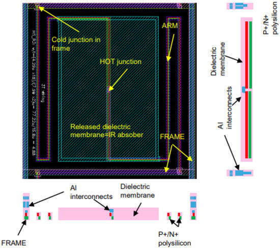
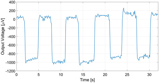
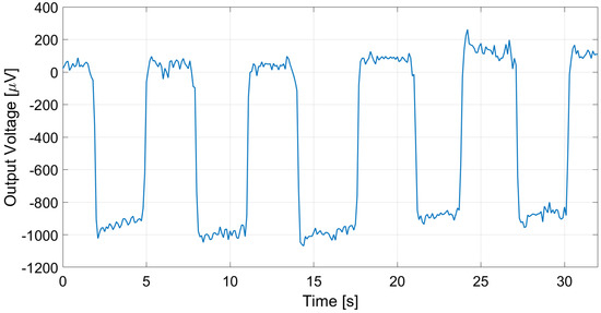
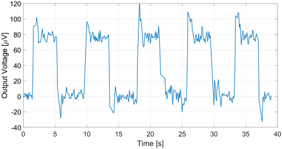
This paper presents a detailed analysis of a micromachined thermopile detector featuring high responsivity and a versatile mosaic structure, based on 128 60 µm × 60 µm pixels connected in series and/or in parallel. The mosaic structure is based on the one employed for the thermal sensor known as TMOS, which consists of a CMOS-SOI transistor embedded in a suspended and thermally isolated absorbing membrane, released through microelectro mechanical system (MEMS) post-processing. Two versions of the thermopile detector, featuring different series/parallel connections, are presented and were experimentally characterized. The most performant of the two achieved 2.7 × 10
(This article belongs to the Special Issue Microsensors and Microsystems for the Human Body)
▼
Show Figures
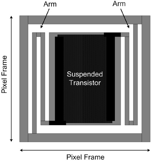
Figure 1


