


Micromachines 2024, 15(5), 574; https://doi.org/10.3390/mi15050574 (registering DOI) - 26 Apr 2024
Abstract
The effect of sand and dust pollution on the sensitive structures of flow sensors in microelectromechanical systems (MEMS) is a hot issue in current MEMS reliability research. However, previous studies on sand and dust contamination have only searched for sensor accuracy degradation due
[...] Read more.
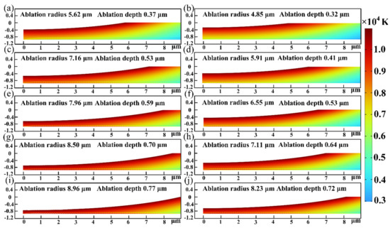
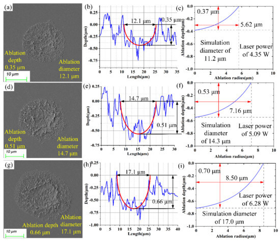
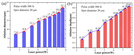
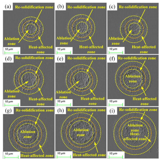
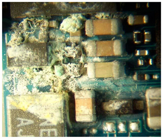
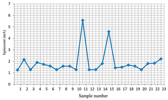
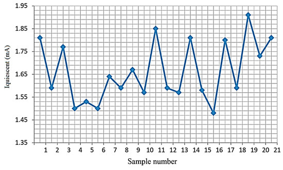
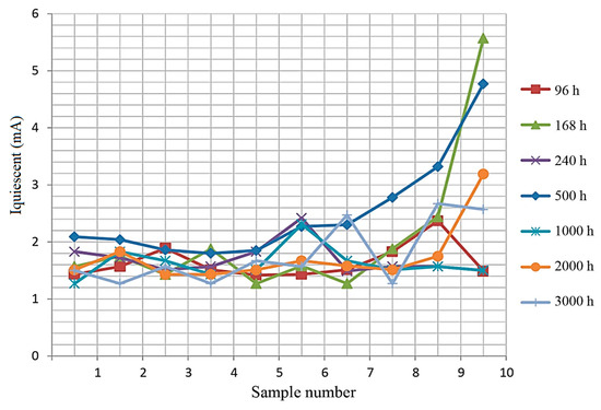
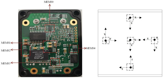
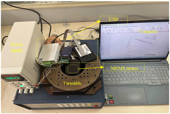
The effect of sand and dust pollution on the sensitive structures of flow sensors in microelectromechanical systems (MEMS) is a hot issue in current MEMS reliability research. However, previous studies on sand and dust contamination have only searched for sensor accuracy degradation due to heat conduction in sand and dust cover and have yet to search for other failure-inducing factors. This paper aims to discover the other inducing factors for the accuracy failure of MEMS flow sensors under sand and dust pollution by using a combined model simulation and sample test method. The accuracy of a flow sensor is mainly reflected by the size of its thermistor, so in this study, the output value of the thermistor value was chosen as an electrical characterization parameter to verify the change in the sensor’s accuracy side by side. The results show that after excluding the influence of heat conduction, when sand particles fall on the device, the mutual friction between the sand particles will produce an electrostatic current; through the principle of electrostatic dissipation into the thermistor, the principle of measurement leads to the resistance value becoming smaller, and when the sand dust is stationary for some time, the resistance value returns to the expected level. This finding provides theoretical guidance for finding failure-inducing factors in MEMS failure modes.
Full article
(This article belongs to the Special Issue Selected Papers From the 25th Annual Conference and 14th International Conference of Chinese Society of Micro-Nano Technology (CSMNT 2023))


