Article

Multi-Threshold Dual-Spacer Dual-Rail Delay-Insensitive Logic (MTD3L): A Low Overhead Secure IC Design Methodology

1
Department of Computer Science and Computer Engineering, University of Arkansas; Fayetteville, AR 72701, USA
2
Department of Electrical and Computer Engineering, North Dakota State University; Fargo, ND 58108, USA
*
Author to whom correspondence should be addressed.
J. Low Power Electron. Appl. 2013, 3(4), 300-336; https://doi.org/10.3390/jlpea3040300
Submission received: 6 August 2013 / Revised: 20 September 2013 / Accepted: 12 October 2013 / Published: 25 October 2013

Abstract

:
As portable devices become more ubiquitous, data security in these devices is becoming increasingly important. Traditional circuit design techniques leave otherwise secure systems vulnerable due to the characteristics of the hardware implementation, rather than weaknesses in the security algorithms. These characteristics, called side-channels, are exploitable because they can be measured and correlated with processed data, potentially giving an attacker insight into the device’s secret data. Alternative design techniques such as dual-rail asynchronous designs are capable of minimizing these potential side-channels by decoupling them from the data being processed. However, these techniques are either expensive to implement compared to standard designs or leave exploitable imbalances in the dual-rail implementation itself. Multi-Threshold Dual-Spacer Dual-Rail Delay-Insensitive Logic (MTD3L) offers security by balancing side-channels both in general and between the dual-rail signals themselves, as well as reduction in circuit overhead compared to previous secure design techniques. Results show that the Advanced Encryption Standard (AES) cores designed using MTD3L exhibit similar security to previous secure techniques with substantially less area and energy overhead.

Graphical Abstract

1. Introduction

As technology advances, more and more electronic devices store secret information such as bank accounts, identification numbers, passwords, and other private data that need to be secured from unauthorized access. Although originally considered safe and secure, hardware, just as software, is prone to attacks that force the targeted system to reveal sensitive data. Cryptographic algorithms are commonly used to protect such data. However, despite the mathematical robustness of these algorithms, their physical implementations are known to be susceptible to attacks. Non-invasive attacks on such devices take advantage of side-channel information leaked from the system, instead of trying to reverse engineer it. Such side-channel information can be power, timing, electromagnetism, and any other information that might be measured from the device during computation.
Most electronic devices running cryptographic algorithms are implemented in CMOS technology, where transistors act as voltage-controlled switches. While a circuit node is switching, electrons flow across the corresponding transistors to charge/discharge its load capacitance, thereby consuming power. Due to the fact that different transistors will be turned on/off while processing different data, causing different power consumption, power-based side­channel attacks can be implemented using the IC’s transient power data. These types of power-based attacks include Differential Power Analysis (DPA) [1], and Correlation Power Analysis (CPA) [2] (which uses the Pearson product-moment correlation coefficient to guess a key). In general, these attacks acquire transient power data while the target IC performs encryption/decryption on different texts, and then use statistical algorithms to derive the key. Power-based attacks are the most powerful and prevalently implemented side-channel attacks [3], and have been successfully implemented to crack almost all cryptographic algorithms on different platforms [4,5,6,7,8,9,10,11,12]. A number of methods have been proposed for mitigating power-based attacks by decoupling transient power consumption from the data being processed. Techniques based on balancing power fluctuation include new CMOS logic gates, which go through a full charge/discharge cycle for each data processed [13,14,15,16,17,18]. Other power balancing methods include modifying the algorithm execution [19], compensating current at the power supply node [20], and using sub-threshold operation [21]. Additionally, many techniques for randomizing power data have been proposed [22,23,24,25,26,27].
The principle of timing-based attacks [28] is very similar to power-based ones except these attacks rely on timing fluctuations of the target circuit while processing different data patterns. Depending on the load capacitance and driving strength, the charge/discharge process during the switching activities at an internal circuit node will take different amounts of time to finish, which in turn causes different timing delays. Existing countermeasures include inserting dummy operations [29], using redundant representation [30], and unifying the multiplication operands [31].
Asynchronous circuits, especially dual-rail asynchronous circuits, possess unique characteristics that could help mitigate such attacks [32,33,34,35,36,37]. Dual-rail asynchronous circuits, such as NULL Convention Logic (NCL) [38], use two wires to represent one signal. The DATA­spacer alternation protocol ensures the number of switching of each signal to be independent from the input; instead, it is only determined by the number of data processed [39], making power variation significantly smaller than synchronous designs [40]. Nonetheless, switching activity remains unbalanced between the two rails of each signal, which most likely drive different capacitive loads; thus, DPA, High-Order DPA, or CPA can still succeed. Moreover, such dual­rail logic circuits are even more vulnerable to timing-based attacks due to their strong data­timing dependency.
To alleviate these issues, Dual-Spacer Dual-Rail Delay­Insensitive Logic (D3L) was developed in [41] as an extension of NCL, which was capable of mitigating both power­ and timing-based side-channel attacks. However, this increased security was gained at the cost of more than four times the area of the base synchronous circuit and almost twice the area of the NCL version. This paper details the design, implementation, and analysis of MTD3L, developed by combining the D3L paradigm with Multi-Threshold NULL Convention Logic (MTNCL) [42,43], resulting in a circuit design methodology that is just as secure as D3L, while requiring slightly more than half the area and energy compared to D3L.
The remainder of this paper is organized as follows. Section 2 presents an overview of the pertinent previous work, including NCL, MTNCL, and D3L. Section 3 details the MTD3L circuit design method. Section 4 presents AES core implementations using MTD3L, as well as versions implemented using D3L, NCL, and the standard synchronous technique. Section 5 details the simulation setups for determining resistance against side-channel attacks, and presents and analyzes the simulation results. Section 6 draws conclusions and provides direction for future work.

2. Previous Work

2.1. NULL Convention Logic (NCL)

NCL [38] is a commonly used delay-insensitive (DI) asynchronous logic design style, which utilizes a multi-rail one-hot scheme, such as dual-rail, to encode data. A dual-rail signal, D, consists of two wires or rails, D0 and D1, which may assume any value from the set {DATA0, DATA1, NULL}, as depicted in Table 1. The DATA0 state corresponds to a Boolean logic 0, the DATA1 state corresponds to a Boolean logic 1, and the NULL state corresponds to the empty set (meaning that the value of D is not yet available). The two rails are mutually exclusive, such that both rails can never be asserted simultaneously; this state is defined as an illegal state.
Table 1. Dual-rail signal.
StateD0D1
NULL00
DATA010
DATA101
Illegal11
NCL circuits are comprised of 27 fundamental gates, which constitute the set of all functions consisting of four or fewer variables [43]. Since each rail of an NCL signal is considered a separate variable, a four variable function is not the same as a function of four literals, which would consist of eight variables for dual-rail logic (e.g., a literal includes both a variable and its complement, F and F’, whereas NCL rails are never complemented, such that a dual-rail NCL signal, F, consists of two variables, F1 and F0, where F0 is equivalent to 
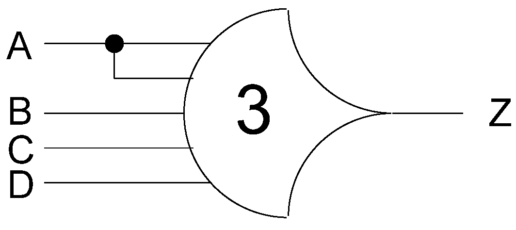
F’). The primary type of threshold gate, shown in Figure 1, is the THmn gate, where 1 ≤ mn. THmn gates have n inputs. At least m of the n inputs must be asserted before the output will become asserted. In a THmn gate, each of the n inputs is connected to the rounded portion of the gate; the output emanates from the pointed end of the gate; and the gate’s threshold value, m, is written inside of the gate.
Figure 1. THmn threshold gate.
Jlpea 03 00300 g001
Another type of threshold gate is referred to as a weighted threshold gate, denoted as THmn w, w1, w2, …, wR. Weighted threshold gates have an integer value, mwR > 1, applied to input R. Here, 1 ≤ R < n; where n is the number of inputs; m is the gate’s threshold; and w1, w2, …, wR, each >1, are the integer weights of input1, input2, …, inputR, respectively. For example, consider the TH34W2 gate, whose n = 4 inputs are labeled A, B, C, and D, shown in Figure 2. The weight of input A, W(A), is therefore 2. Since the gate’s threshold, m, is 3, this implies that in order for the output to be asserted, either inputs B, C, and D must all be asserted, or input A must be asserted along with any other input, B, C, or D.
Figure 2. TH34w2 threshold gate: Z = AB + AC + AD + BCD.
Jlpea 03 00300 g002
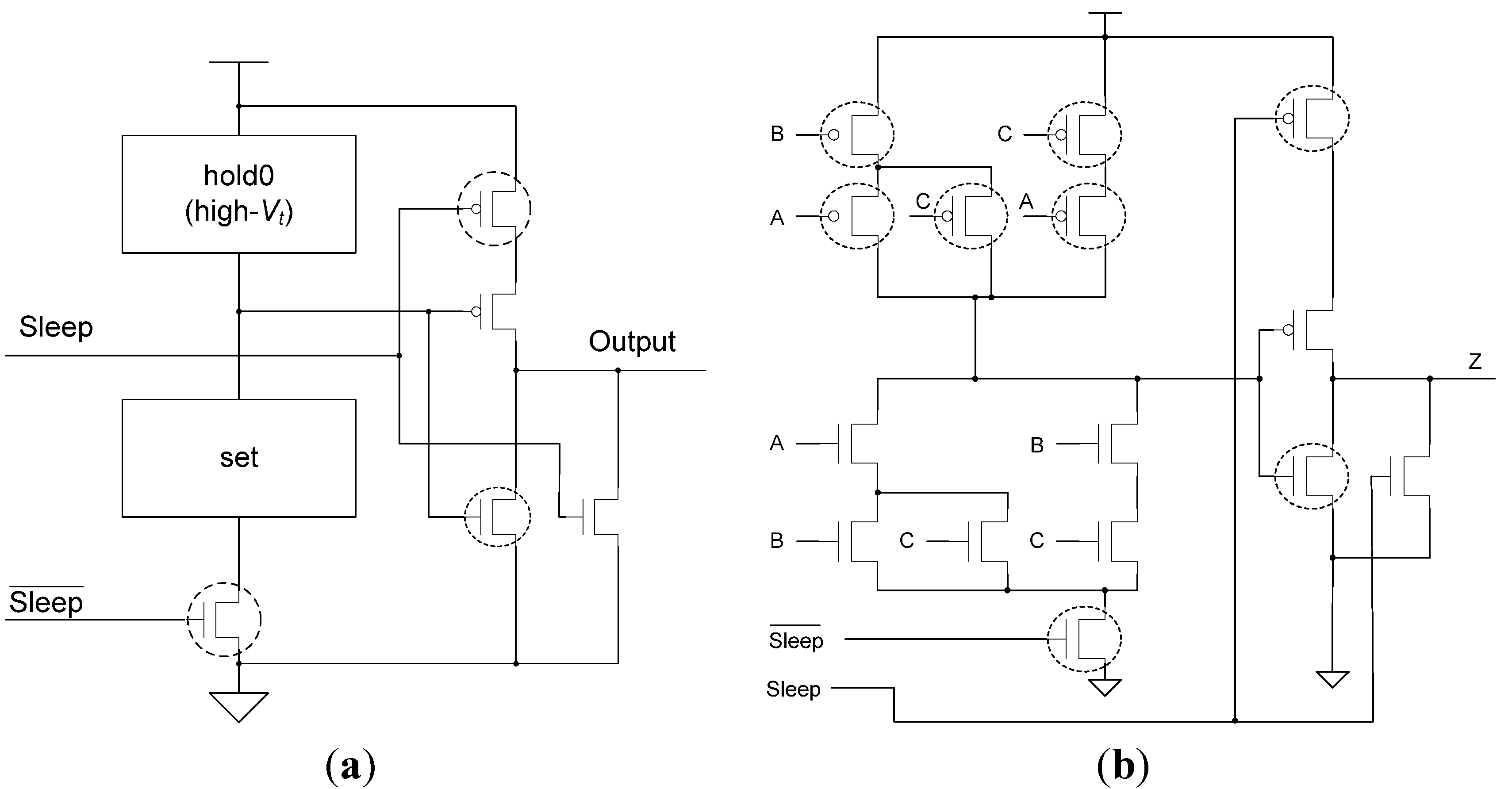
NCL threshold gates are designed with hysteresis state-holding capability, such that after the output is asserted, all inputs must be deasserted before the output will be deasserted. Hysteresis ensures a complete transition of inputs back to NULL before asserting the output associated with the next wavefront of input data. Therefore, a THnn gate is equivalent to an n-input C-element (i.e., when all inputs are asserted the output is asserted; the output then remains asserted until all inputs are deasserted, at which time the output becomes deasserted) [44]; and a TH1n gate is equivalent to an n-input OR gate. NCL threshold gates may also include a reset input to initialize the output. Circuit diagrams designate resettable gates by either a d or an n appearing inside the gate, along with the gate’s threshold. d denotes the gate as being reset to logic 1; n, to logic 0. These resettable gates are used in the design of DI registers.
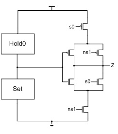
To achieve hysteresis state-holding capability, NCL gates have both set and hold equations, where the set equation determines when the gate will become asserted and the hold equation determines when the gate will remain asserted once it has been asserted. The set equation determines the gate’s functionality as one of the 27 NCL gates [43], whereas the hold1 equation is simply all inputs ORed together. The general equation for an NCL gate with output Z is: Z = set + (Z- × hold1), where Z- is the previous output value and Z is the new value.
To implement an NCL gate using CMOS technology, an equation for the complement of Z is also required, which in general form is: Z’ = reset + (Z-’ × hold0), where reset is the complement of hold1 (i.e., the complement of each input, ANDed together) and hold0 is the complement of set, such that the gate output is deasserted when all inputs are deasserted, and then remains deasserted while the gate’s set condition is false. The new output value, Z, depends on the previous output value, Z-, which requires internal gate feedback, as shown in 
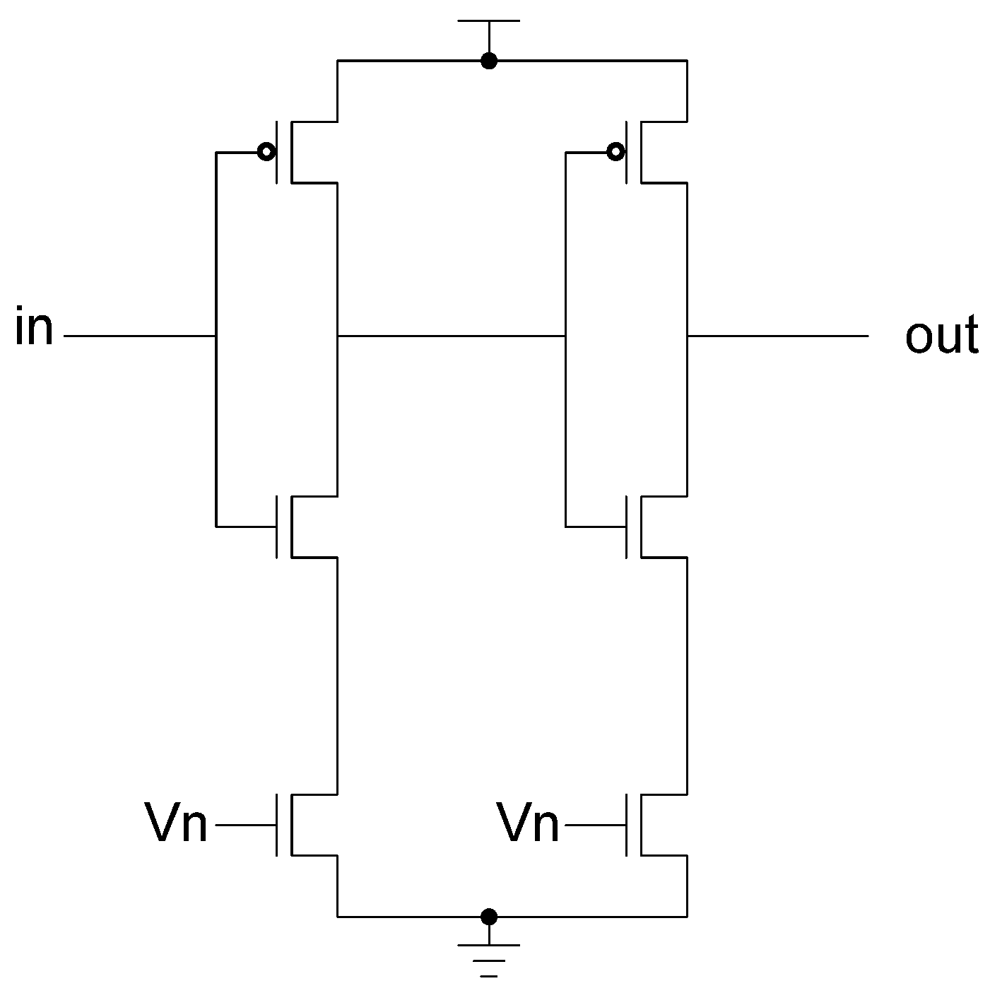
Figure 3, for a static implementation [43].
Figure 3. (a) Static NULL Convention Logic (NCL) gate structure; (b) Static NCL TH23 implementation.
Jlpea 03 00300 g003
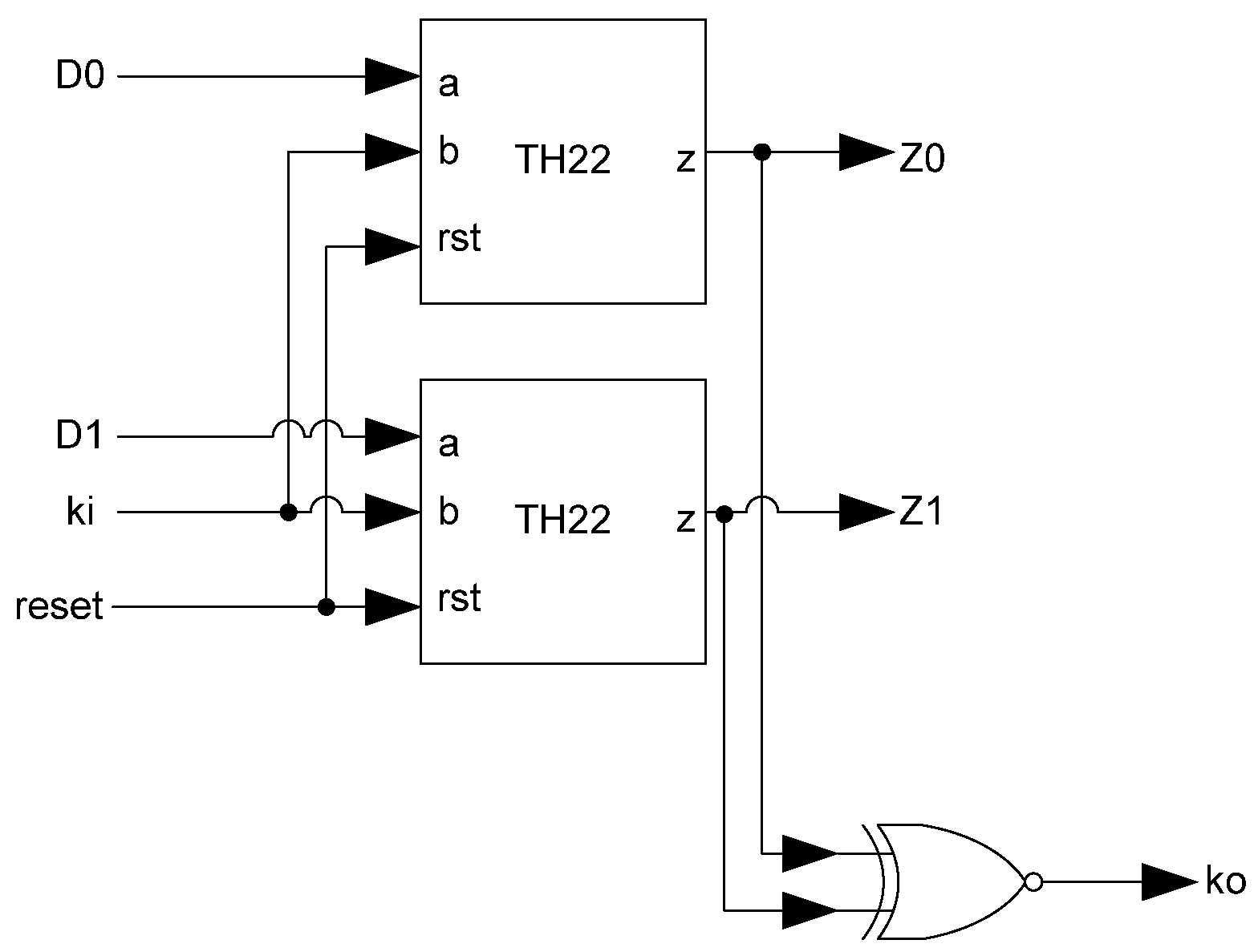
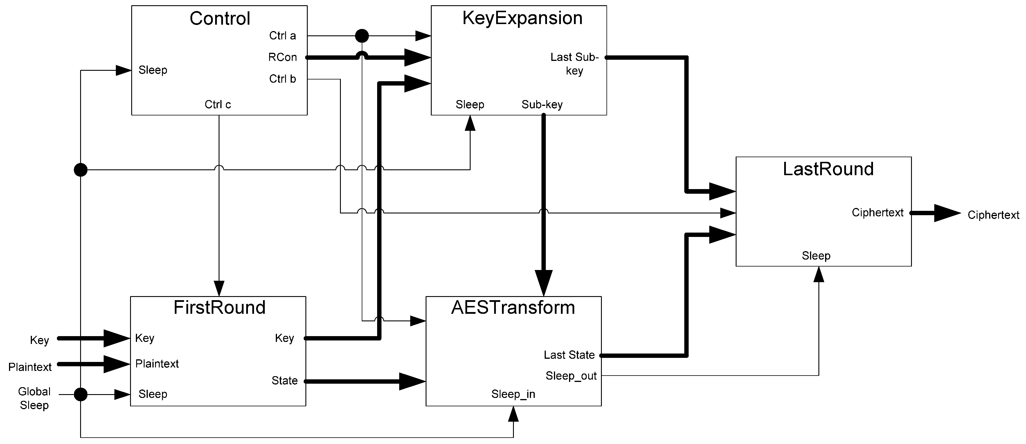
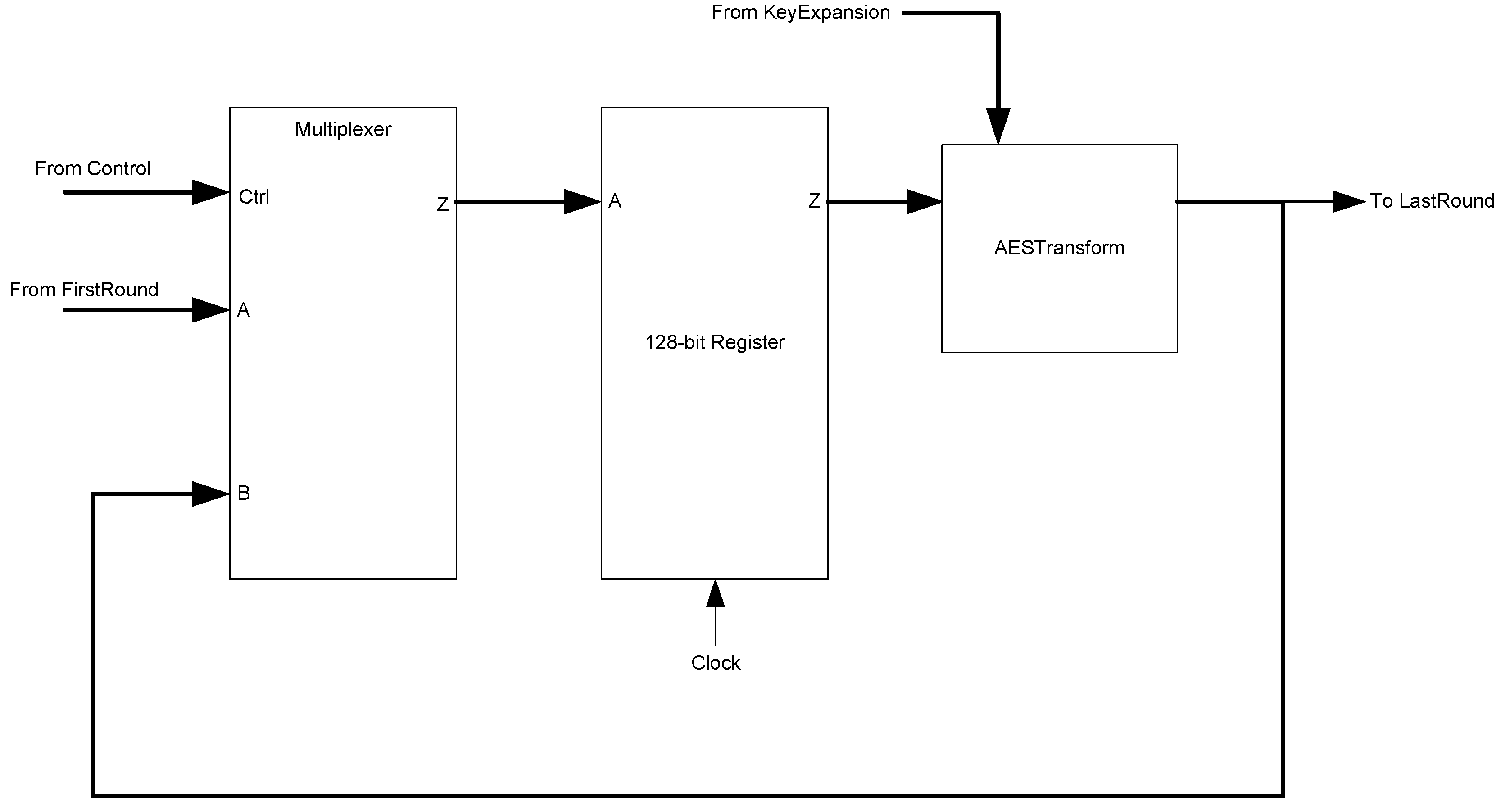
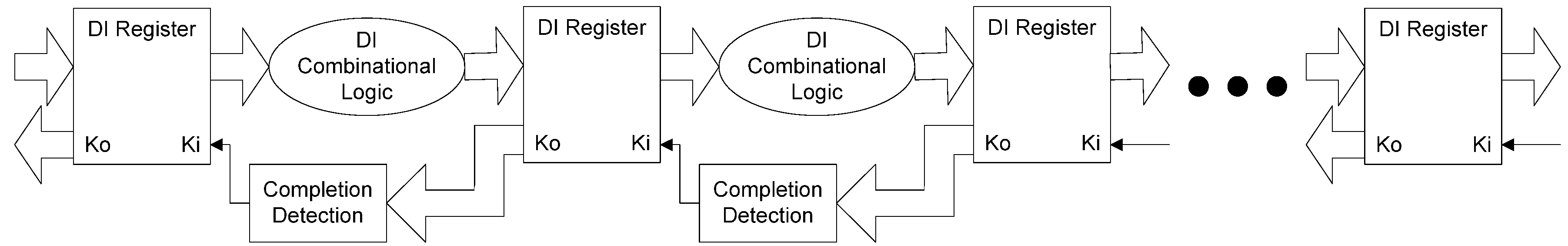
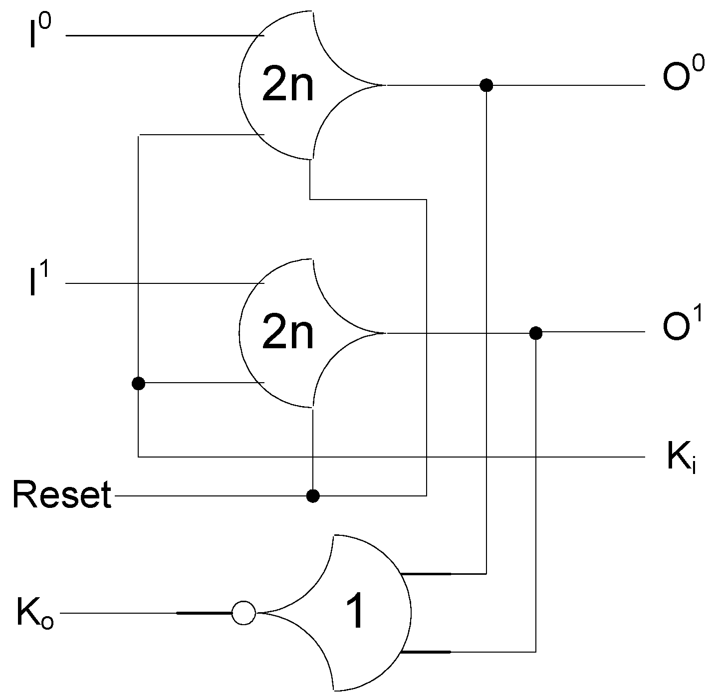
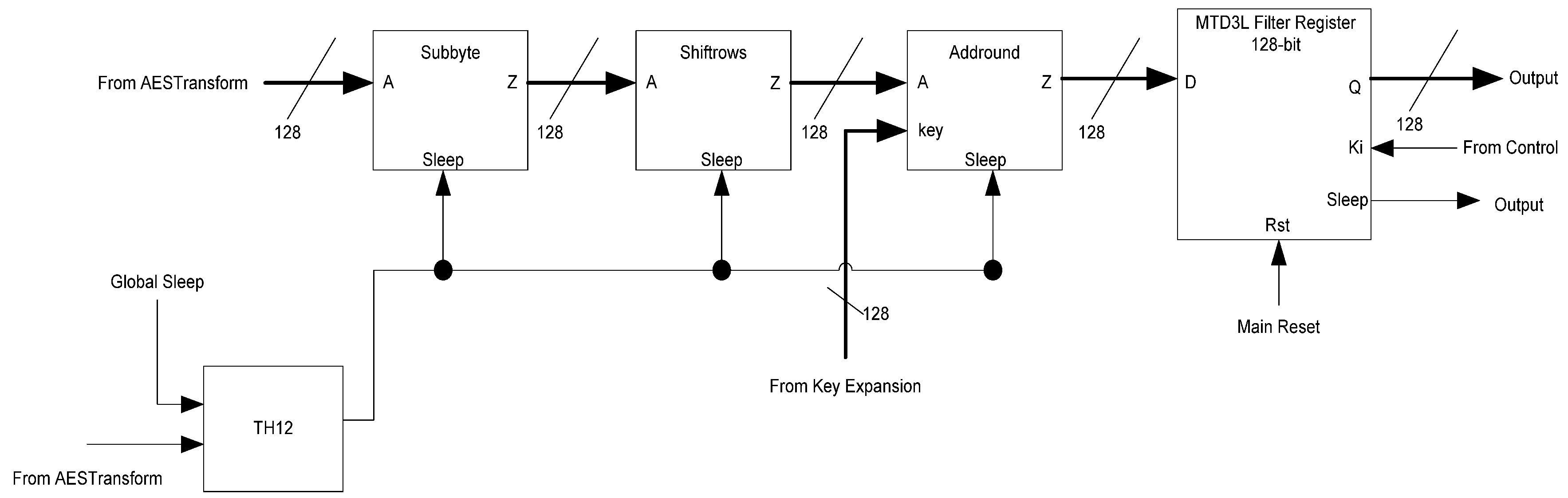
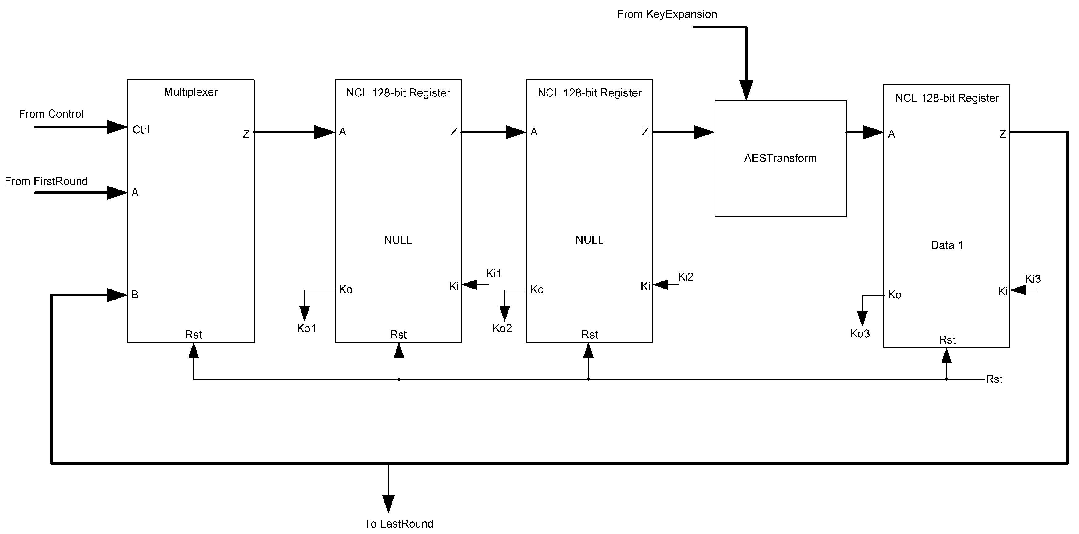
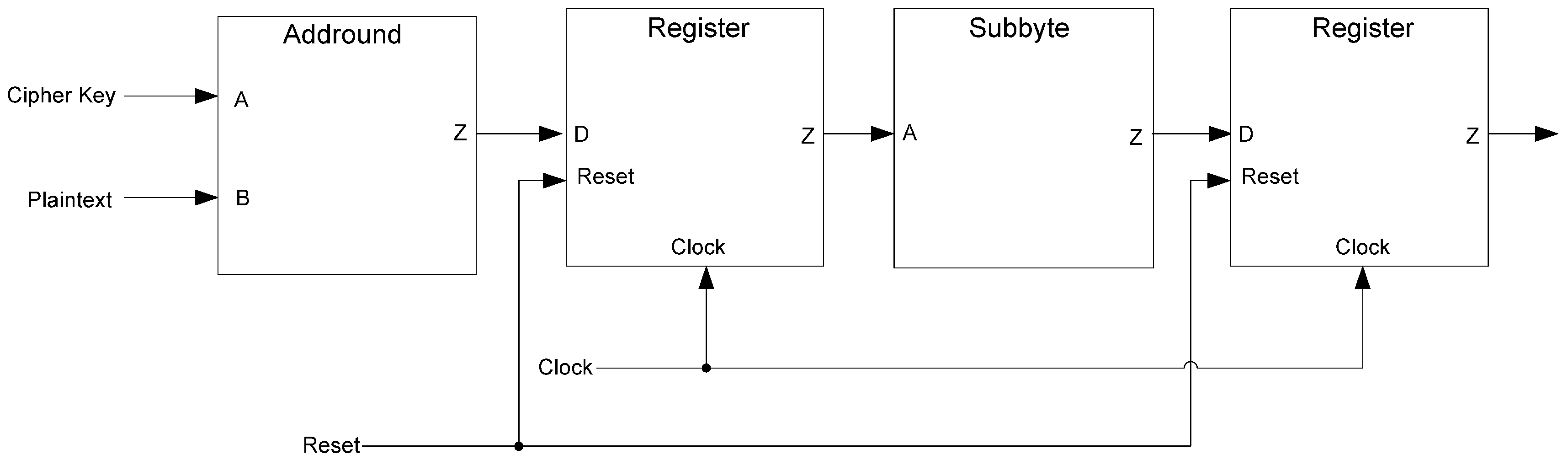
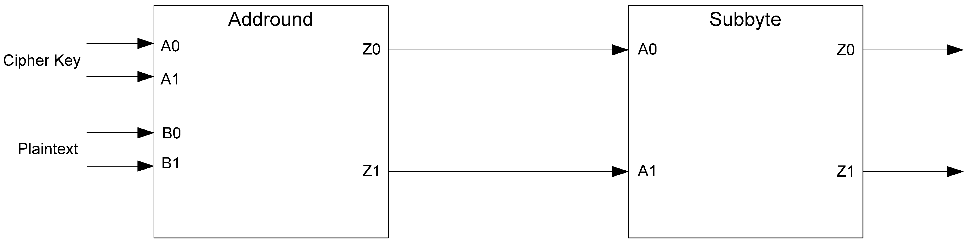
The framework for NCL systems consist of DI combinational logic sandwiched between DI registers, as shown in Figure 4, which is very similar to synchronous systems. NCL systems contain at least two DI registers, one at both the input and at the output. Two adjacent register stages interact through their request and acknowledge signals, Ki and Ko, respectively, to prevent the current DATA wavefront from overwriting the previous DATA wavefront, by ensuring that the two DATA wavefronts are always separated by a NULL wavefront. The acknowledge signals are combined in the Completion Detection circuitry [43] to produce the request signal(s) to the previous register stage. NCL registration is realized through cascaded arrangements of single-bit dual-rail registers, shown in Figure 5, which pass a DATA value at the input only when Ki is request for data (rfd) (i.e., logic 1) and likewise pass NULL only when Ki is request for null (rfn) (i.e., logic 0). They also contain a NOR gate to generate Ko, which is rfn when the register output is DATA and rfd when the register output is NULL.
Figure 4. NCL system framework: input wavefronts are controlled by local handshaking signals and Completion Detection instead of by a global clock signal. Feedback requires at least three DI registers in the feedback loop to prevent deadlock.
Jlpea 03 00300 g004
Figure 5. Single-bit dual-rail register.
Jlpea 03 00300 g005
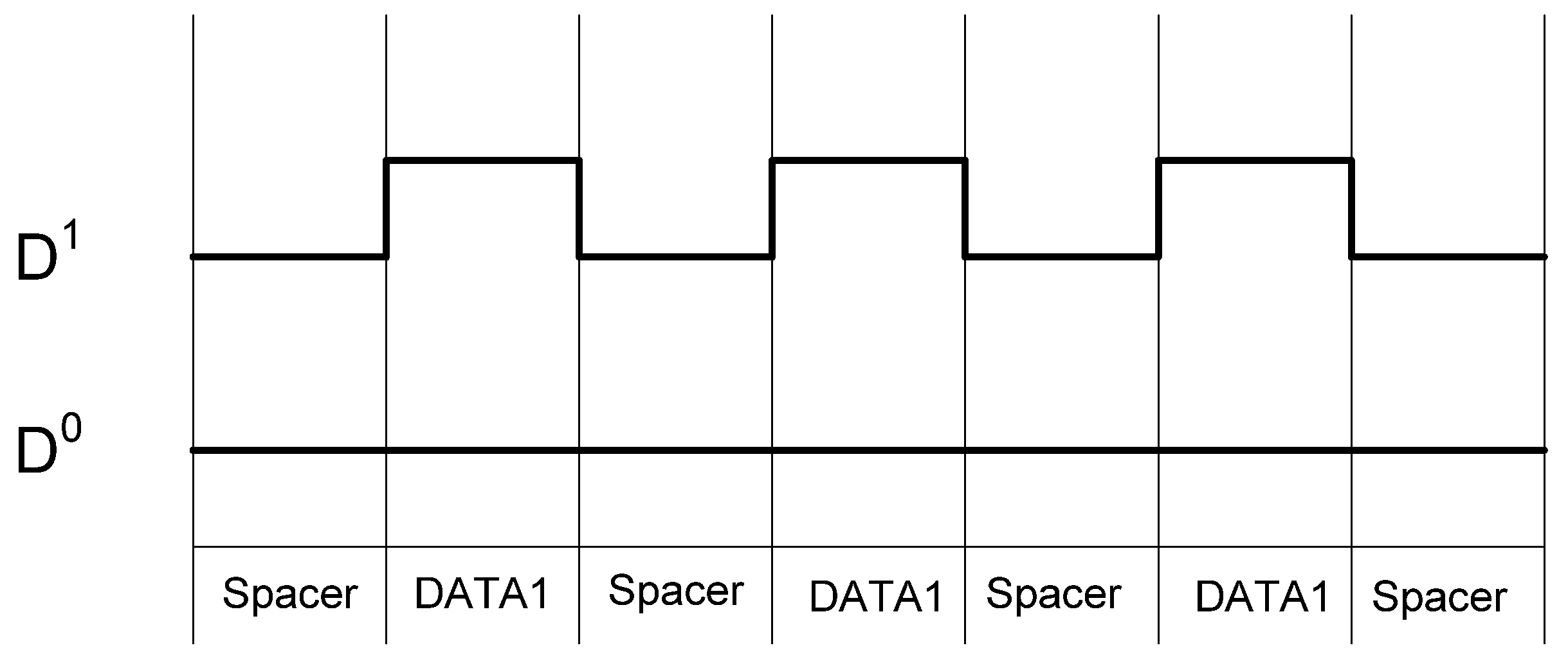
The NCL dual-rail encoding style decouples the relationship between the data being processed and the side-channel characteristics of the circuit, particularly power consumption, giving NCL circuits increased resistance to power related side-channel attacks over synchronous circuits. However, while the overall switching activity of a data bit may be balanced regardless of data, the individual encoding rails are not balanced, as illustrated in Figure 6. Furthermore, if the two rails are driving different capacitance, which is always the case in a large circuit, then attackers may be able to distinguish between the rails, allowing attackers to determine a relationship between the processed data and the circuit’s side-channels.
Figure 6. NCL switching activity for passing consecutive DATA1s.
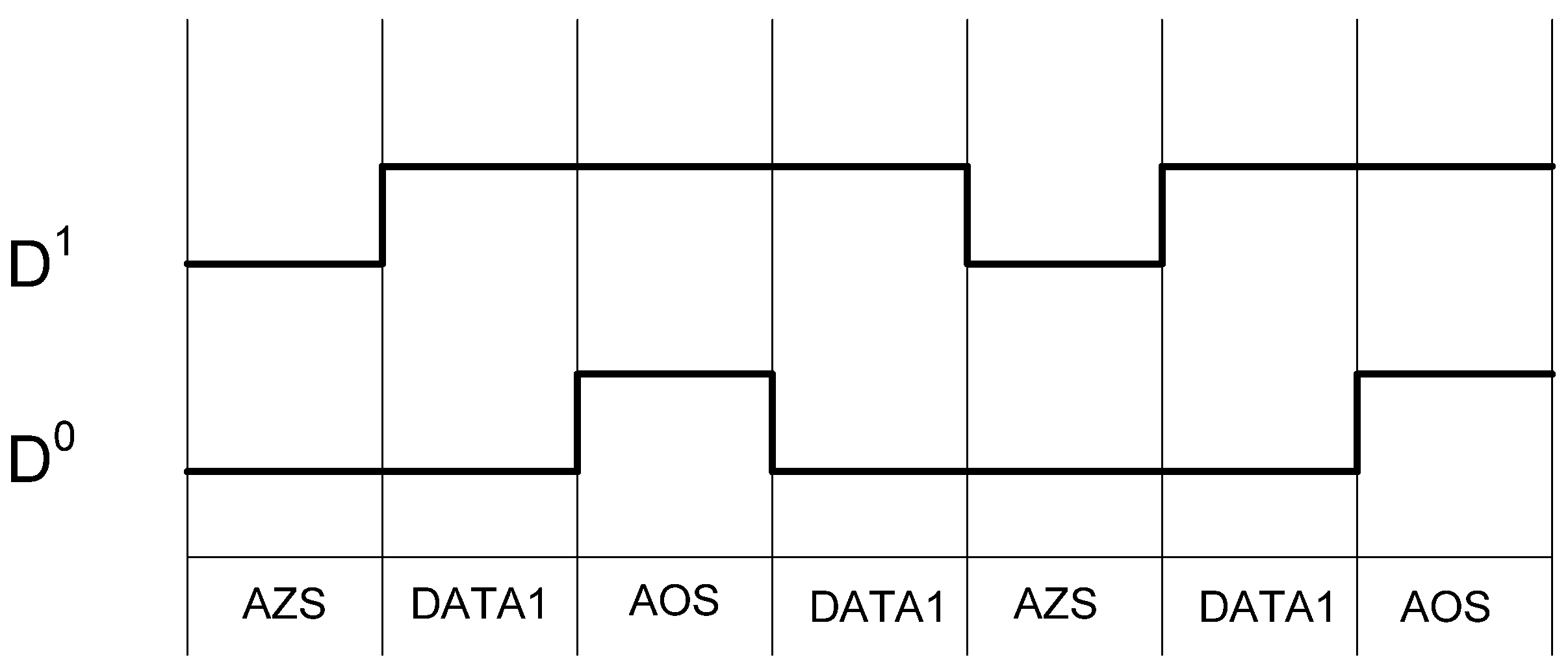
Jlpea 03 00300 g006

2.2. Multi-Threshold NULL Convention Logic (MTNCL)

MTNCL circuits utilize a sleep signal to simultaneously force all circuit elements to NULL instead of propagating a NULL input through the circuit, as described in [42]. This allows for the MTNCL gates to no longer require state-holding hysteresis logic and for the MTNCL combinational logic circuits to no longer need to be input-complete and observable, both of which significantly reduce area and power/energy, while increasing speed. The Static MTNCL (SMTNCL) gate and the Slept Early Completion and Registration Input-Incomplete (SECRII) architecture are shown in Figure 7 and Figure 8, respectively, and are both detailed in [42].
Figure 7. (a) SMTNCL gate structure; (b) SMTNCL TH23 implementation.
Jlpea 03 00300 g007
Figure 8. SECRII architecture with completion logic and registration slept.
Jlpea 03 00300 g008

2.3. Dual-Spacer Dual-Rail Delay­Insensitive Logic (D3L)

D3L is an extension of the NCL logic style that utilizes a dual-spacer protocol, as opposed to NCL’s single spacer protocol [41]. The motivation for this is the elimination of imbalanced switching activity on the two encoding wires of a data bit. By balancing this switching activity, data is further decoupled from the power consumption of the circuit, providing increased robustness against power analysis attacks.
Table 2 shows the D3L encoding scheme. Like NCL, the DATA and NULL states remain the same. However, the NULL state is now called the All-Zero Spacer (AZS); and the former illegal state, where both rails are asserted, is now the All-One Spacer (AOS). The AZS and AOS are alternated between spacer cycles, implementing a dual-spacer protocol. As a result, the switching activity over a complete set of data/spacer cycles is balanced on both rails, as shown in Figure 9.
Table 2. D3L encoding scheme.
StateD0D1
All-Zero Spacer (AZS)00
Data010
Data101
All-One Spacer (AOS)11
Figure 9. D3L switching activity for passing consecutive DATA1s.
Jlpea 03 00300 g009
The D3L threshold gates are modified versions of the NCL threshold gates. As such, the complete set of 27 NCL functions is implemented in D3L. While NCL gates use hysteresis, D3L gates are unable to do so to accommodate the dual-spacer protocol. As such, D3L threshold gates are smaller than NCL threshold gates due to the omission of the hysteresis transistors. The removal of hysteresis, however, means that D3L gates are unable to guarantee input completeness. Instead, the NCL_X technique [45] is used to provide input-completeness. This technique adds additional logic to D3L functions that check the inputs and outputs of each function to create a completion signal. Since the spacer cycles in D
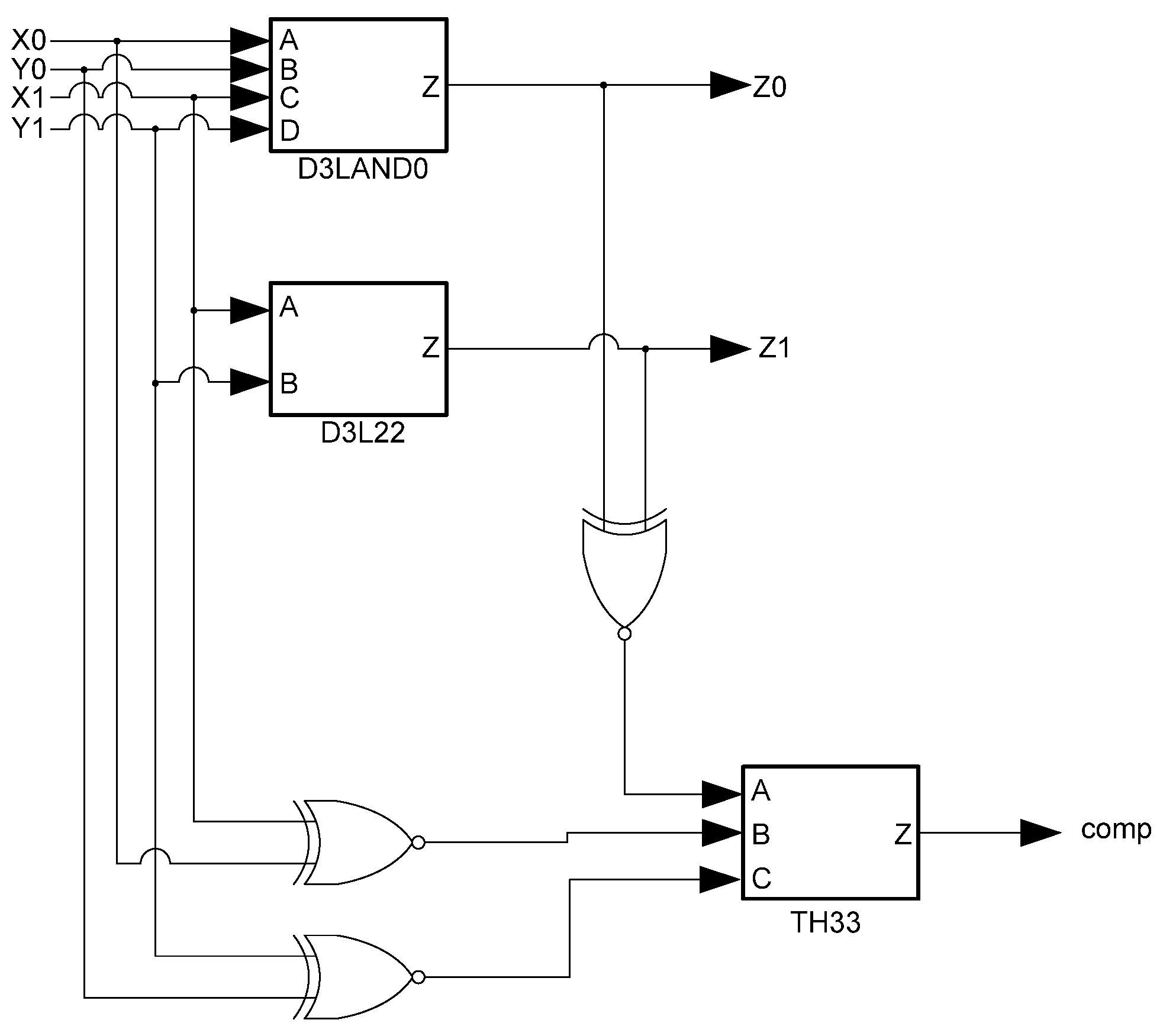
3L occur when data rails are the same, an XNOR gate can be used to detect them. The outputs from these XNOR gates are input to the completion component, along with the usual handshaking signals, to ensure that the logic is ready for the next wavefront. A downside to this technique, however, is the overhead incurred by adding large amounts of XNOR and threshold gates to the design to ensure input-completeness. An input-complete D3L AND function is shown in Figure 10.
Figure 10. D3L input-complete AND function.
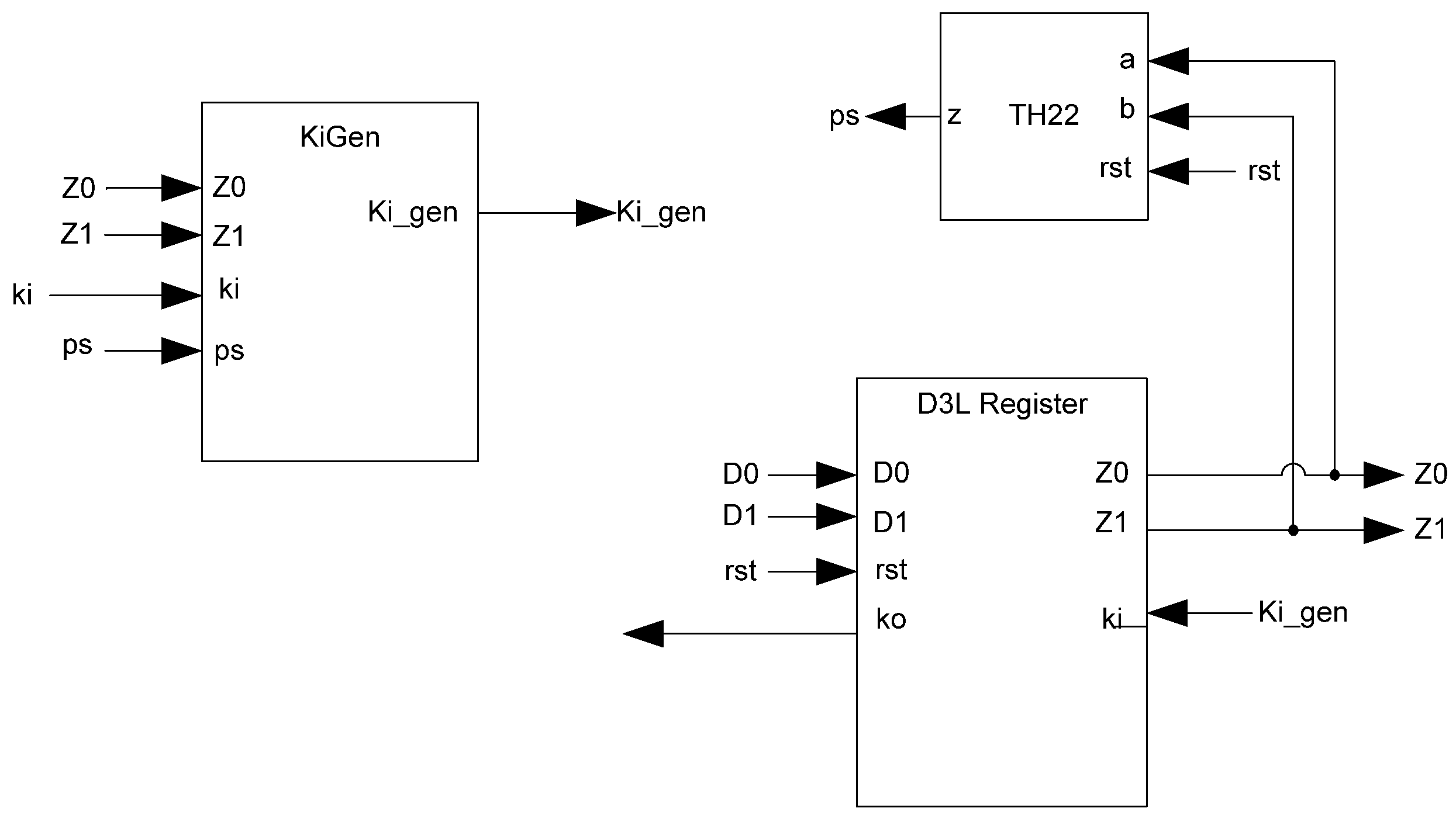
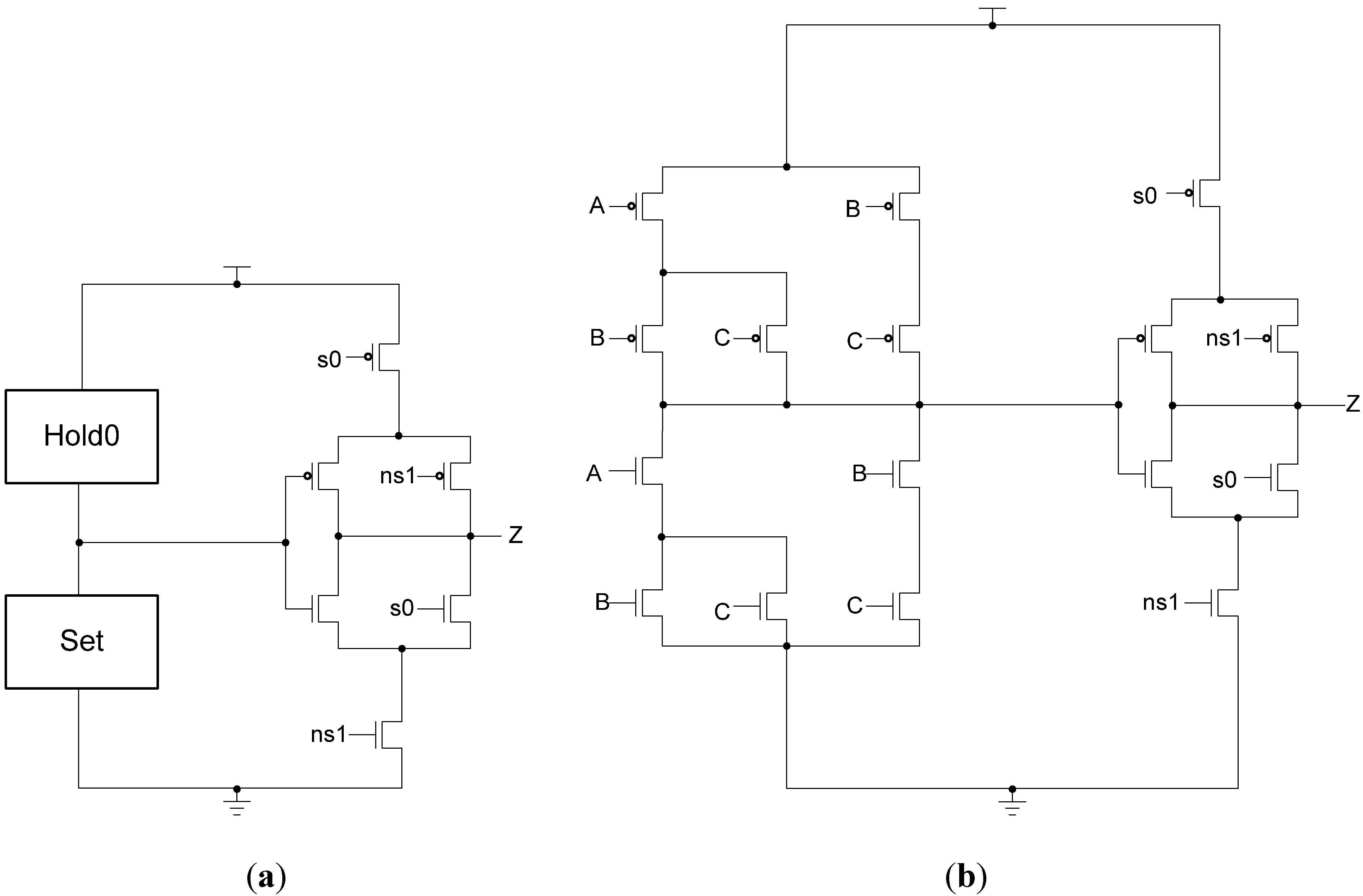
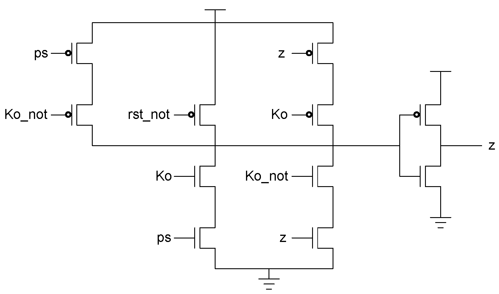
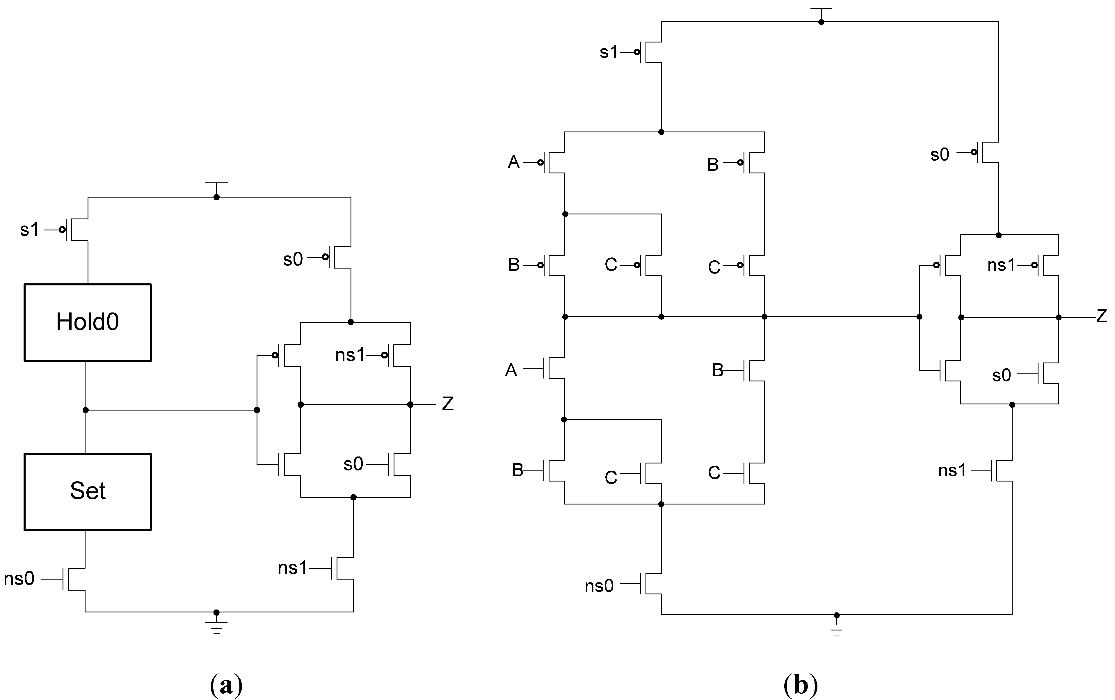
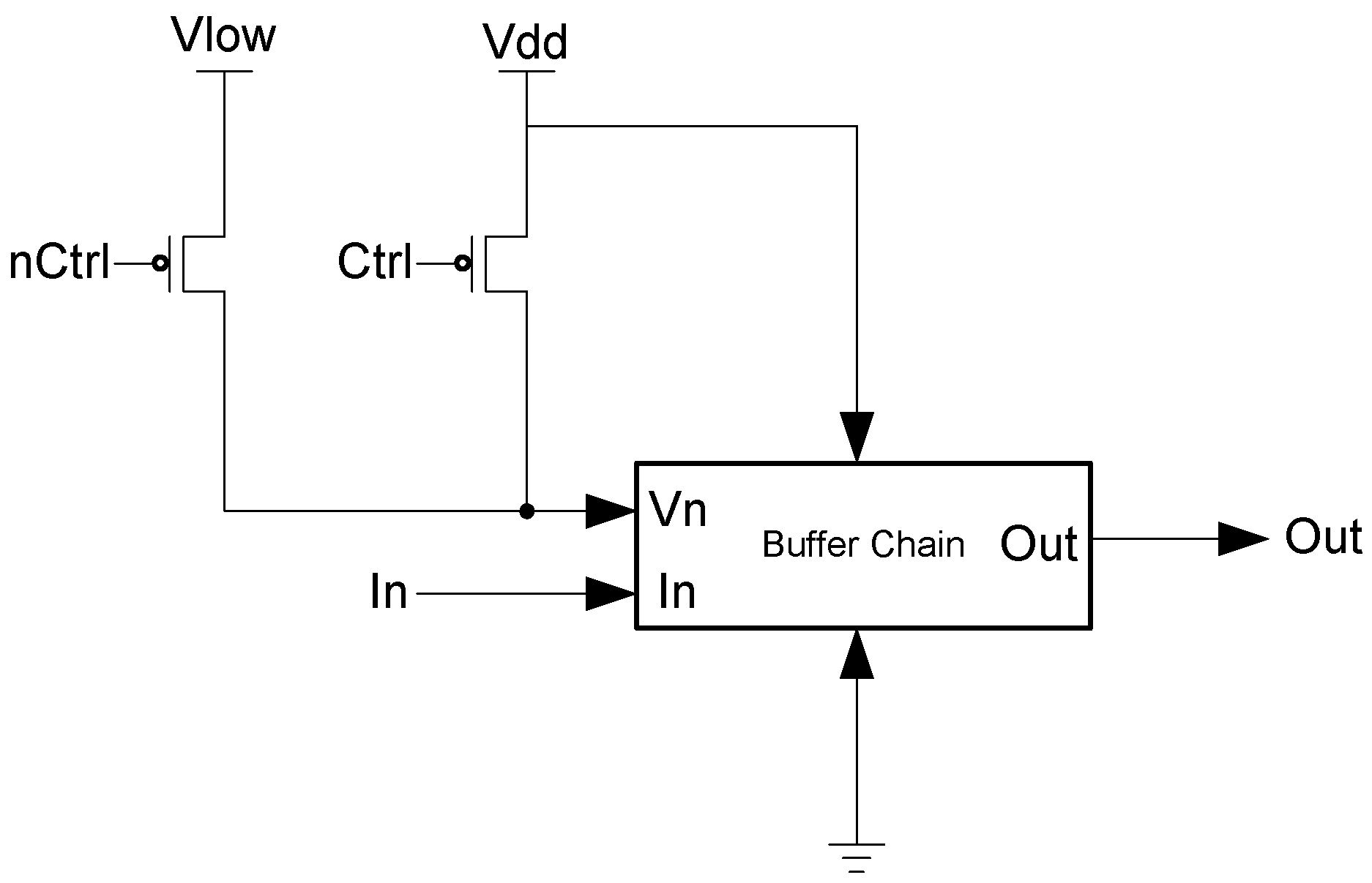
Jlpea 03 00300 g010
The basic D3L Register, shown in Figure 11, is a modified NCL register. It consists of two TH22 gates which are resettable to the desired value. An XNOR gate facilitates Ko generation by checking the relative values of the register’s outputs. As mentioned previously, the XNOR gate is required to detect both AZS and AOS.
Figure 11. D3L register.
Jlpea 03 00300 g011
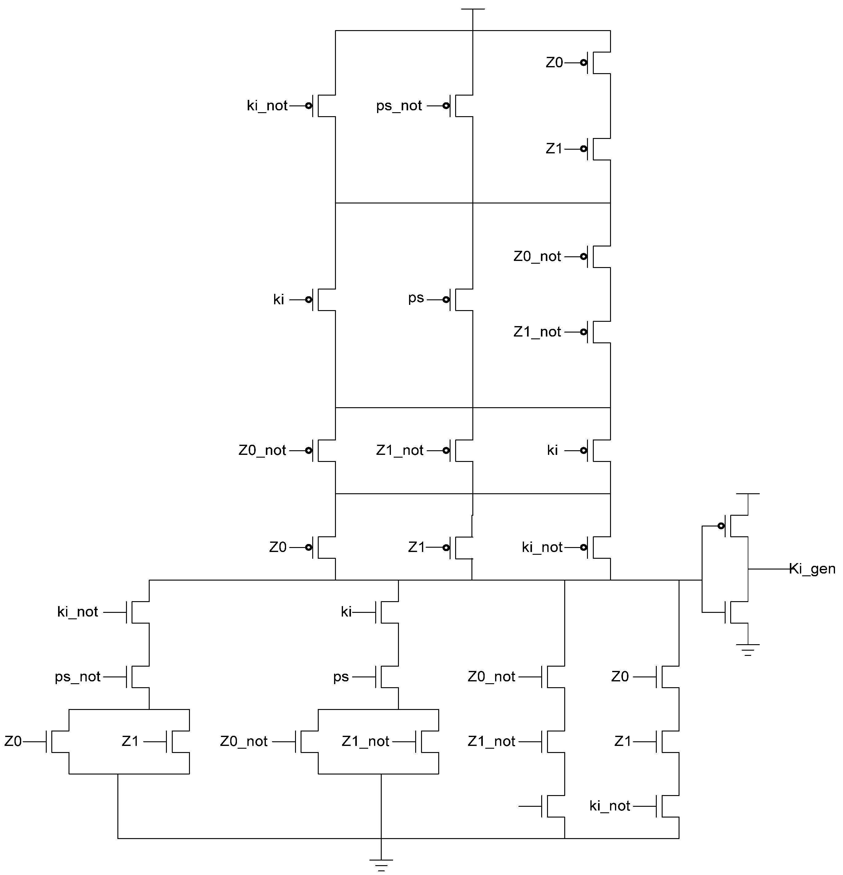
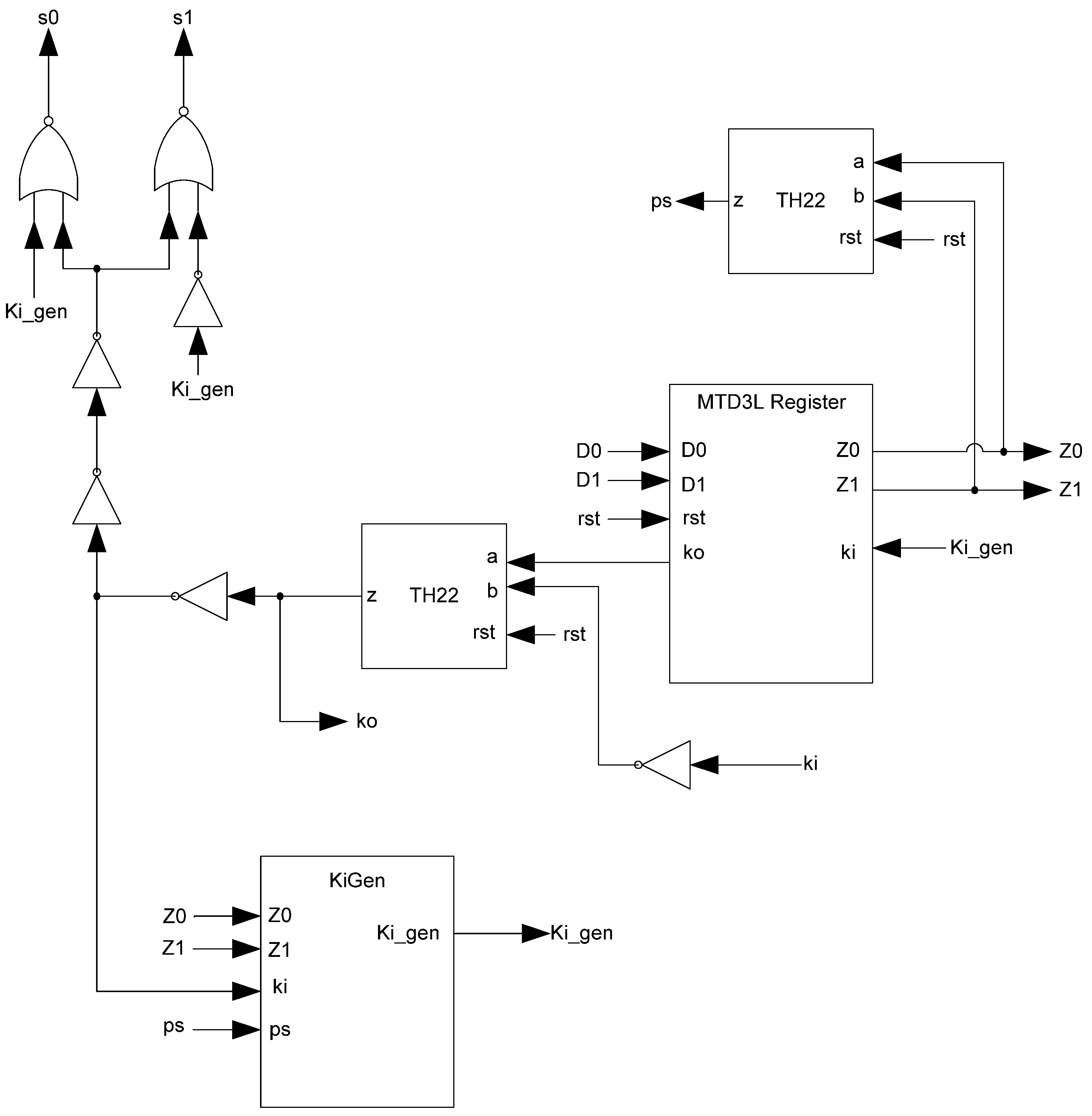
Additional logic is required to facilitate the dual-spacer protocol. NCL registers require a NULL input before they are able to accept new data. They will not recognize an all-one spacer. To fix this, extra logic capable of recognizing the all-one spacer is used to control the register’s Ki input. This Ki Generator has four inputs: the early completion Ki, ps (previous spacer), and the two dual-rail outputs of the register. The value of ps is generated by a resettable TH22 gate. This value is logic 0 for an AZS and logic 1 for an AOS. The ps gate and the register must be reset to the same value. If the register is reset to DATA then the ps gate is reset to logic 0. The Ki Generator’s output follows the Boolean equation Ki_gen = Ki ps (Z0+Z1)+ Ki ps (Z0+Z1)+ Z0 Z1 Ki+Z0 Z1 Ki resulting from the truth table shown in Table 3, yielding the transistor level implementation shown in Figure 12. If an AOS is needed then the value of Ki_gen will be changed to logic 1 allowing the register to latch it. Once the next data value arrives, Ki_gen will switch to logic 0. As a result, one of the register’s TH22 gates will have two low inputs which will change its output to logic 0, latching the data. A complete D3L register is shown in Figure 13.
Table 3. Ki Generator (KiGen) truth table.
RowZ0Z1KipsKi_gen
100000
200010
300101
400111
501001
601010
701100
801111
910001
1010010
1110100
1210111
1311001
1411011
1511100
1611110
Figure 12. KiGen transistor diagram.
Jlpea 03 00300 g012
Figure 13. Complete D3L register.
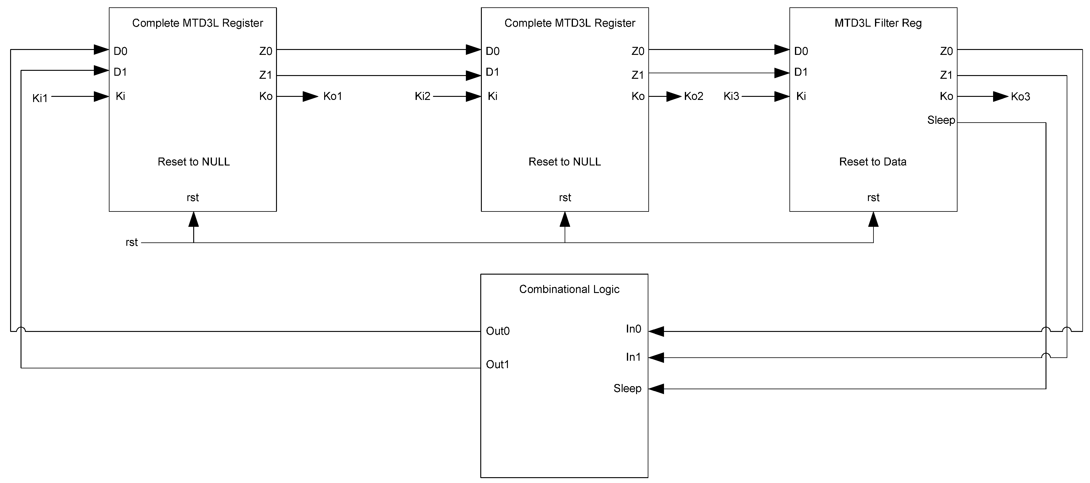
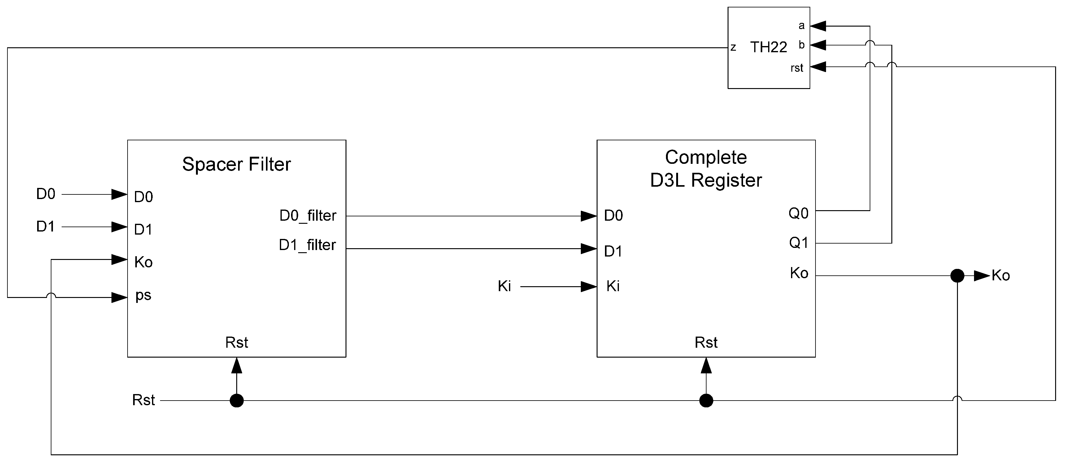
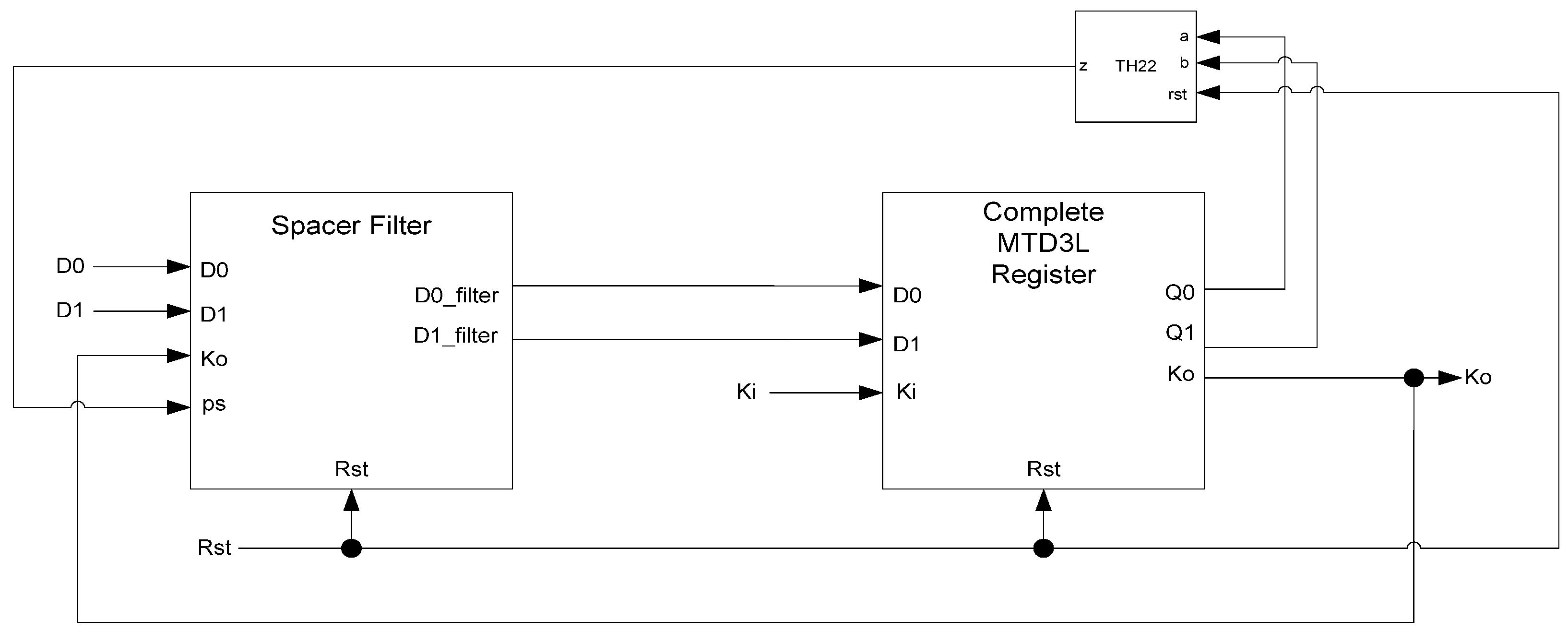
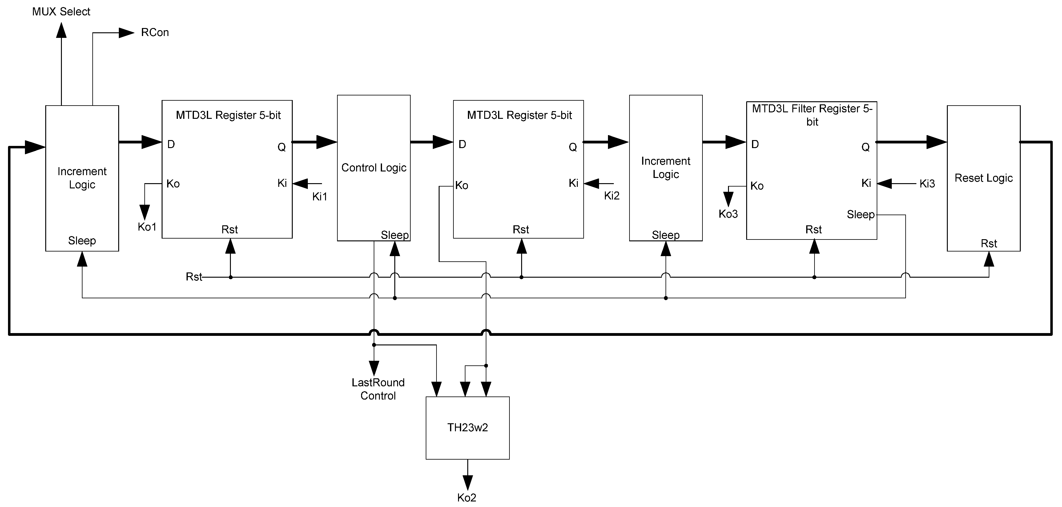
Jlpea 03 00300 g013
While the D3L register is capable of handling the dual-spacer protocol, it is insufficient to implement ring register configurations. This is because a basic D3L register is incapable of generating alternating spacers. Instead, the same spacer would pass through the ring twice causing deadlock. To solve this, a D3L filter register is required for generating alternating spacers, which consists of a basic D3L register with a spacer filter operating on the register’s inputs. The spacer filter monitors the dual-rail input, the previous spacer, and the Ko from the register to ensure that spacers are alternated as they pass through. In a typical ring register configuration, the first two registers would be normal D3L registers reset to NULL and a filter register reset to DATA0 or DATA1. When the filter register receives an AZS or AOS it outputs the alternate spacer. This ensures that the same spacer does not pass through the ring twice. Figure 14 shows the D3L filter register diagram, while 
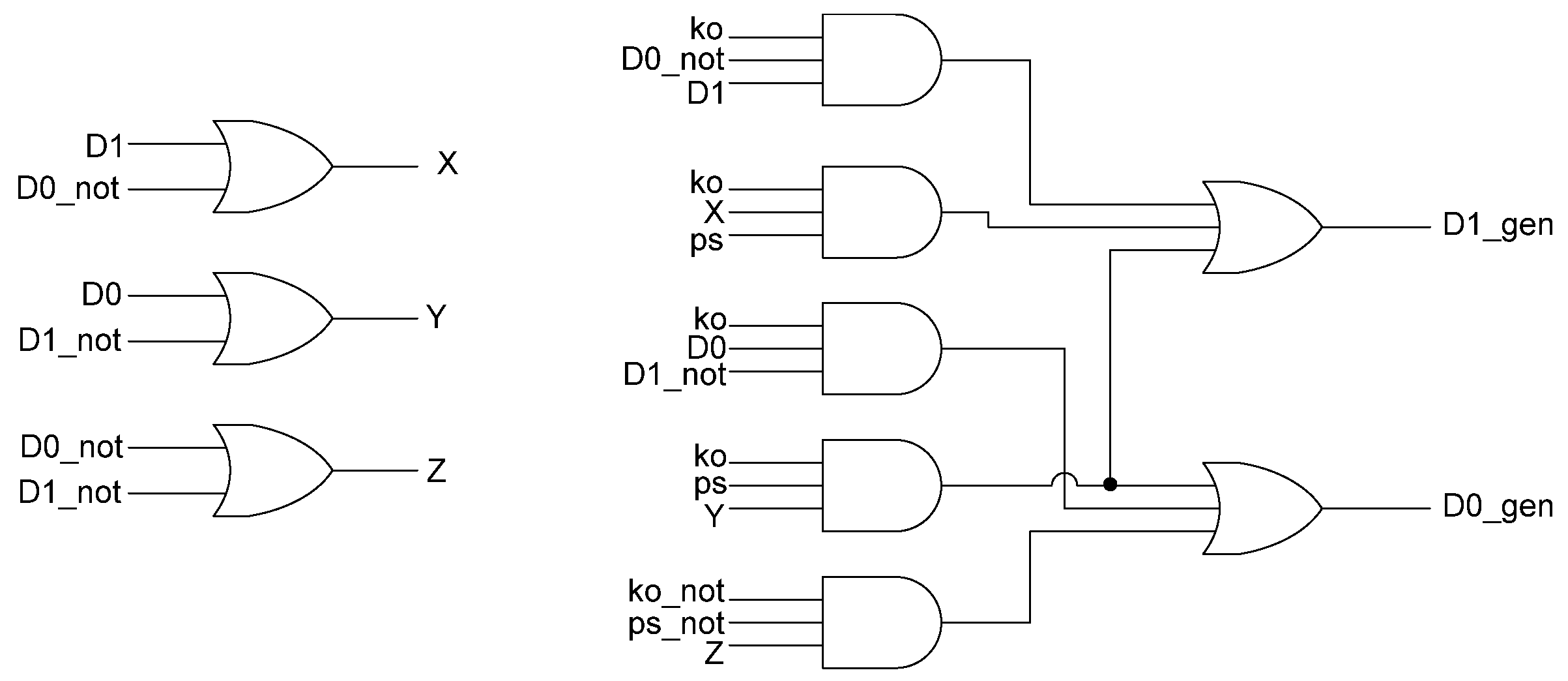
Figure 15 shows the transistor level schematic of the spacer filter, whose outputs are based on the following equations:
D0_filter = D0 D1+Ko ps D0+Ko ps D0+Ko ps D1+Ko ps D1
D1_filter = D0 D1+Ko ps D1+Ko ps D1+Ko ps D0+Ko ps D0
Figure 14. D3L filter register.
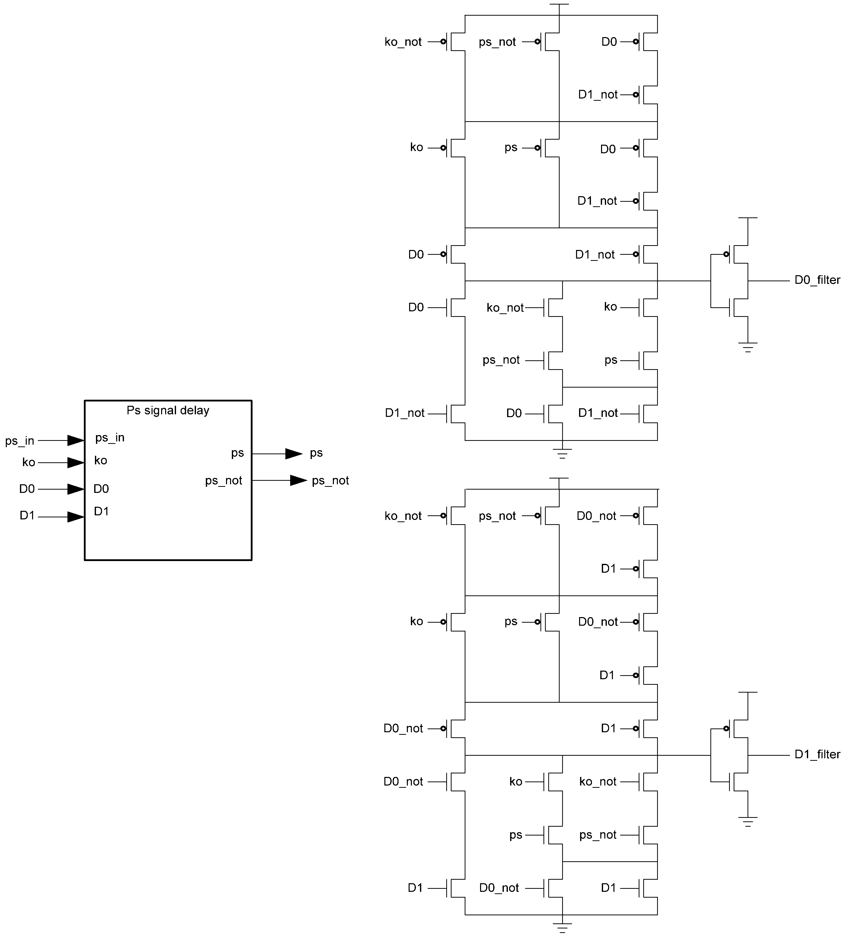
Jlpea 03 00300 g014
Figure 15. Spacer filter transistor level diagram.
Jlpea 03 00300 g015
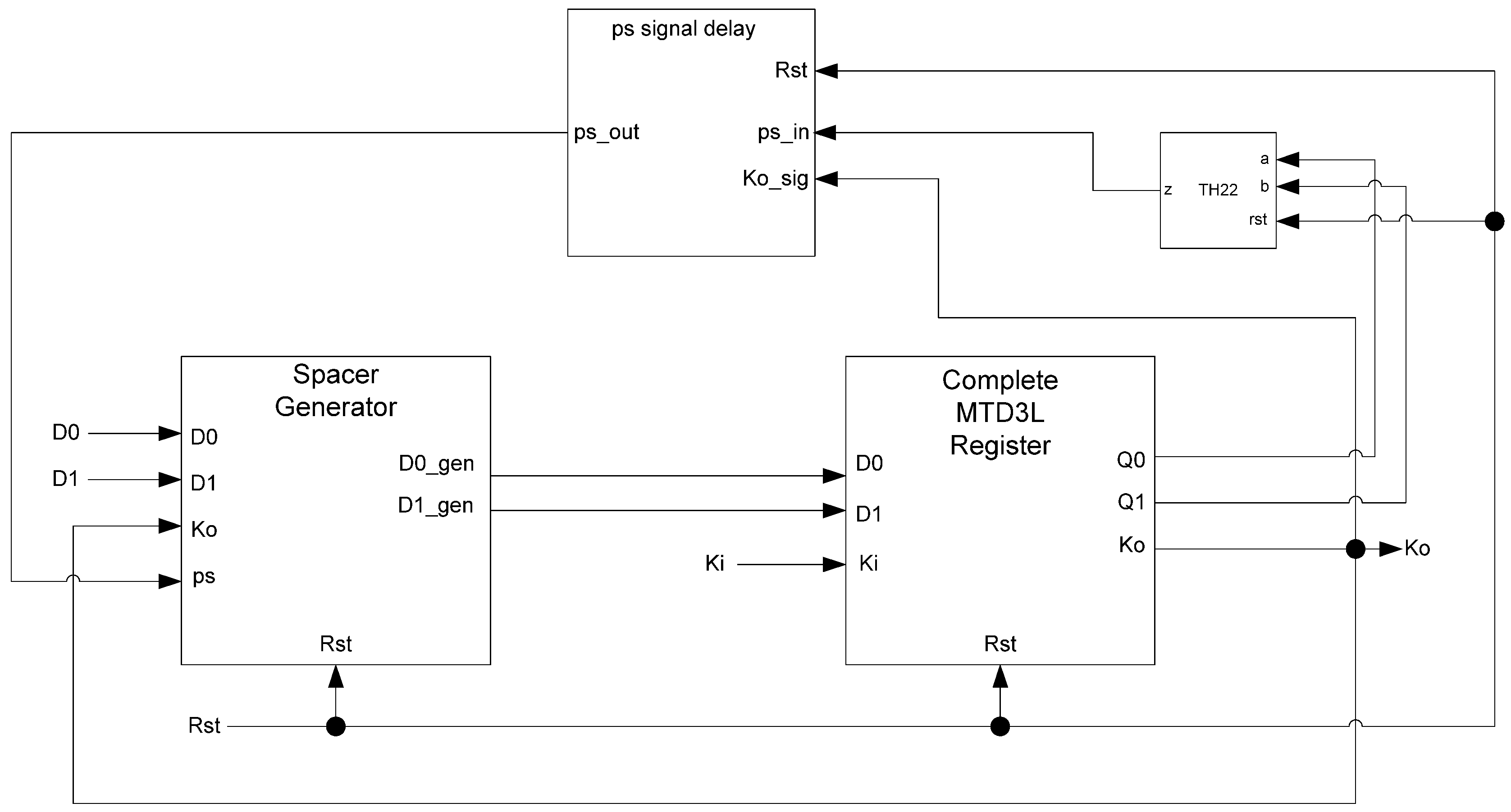
The PS signal delay component used in the spacer filter, shown in Figure 16, prevents ps from changing unless the register’s Ko is logic 1, i.e., requesting DATA. This ensures that the value of ps is only changed once the register receives the spacer.
Figure 16. PS signal delay component.
Jlpea 03 00300 g016
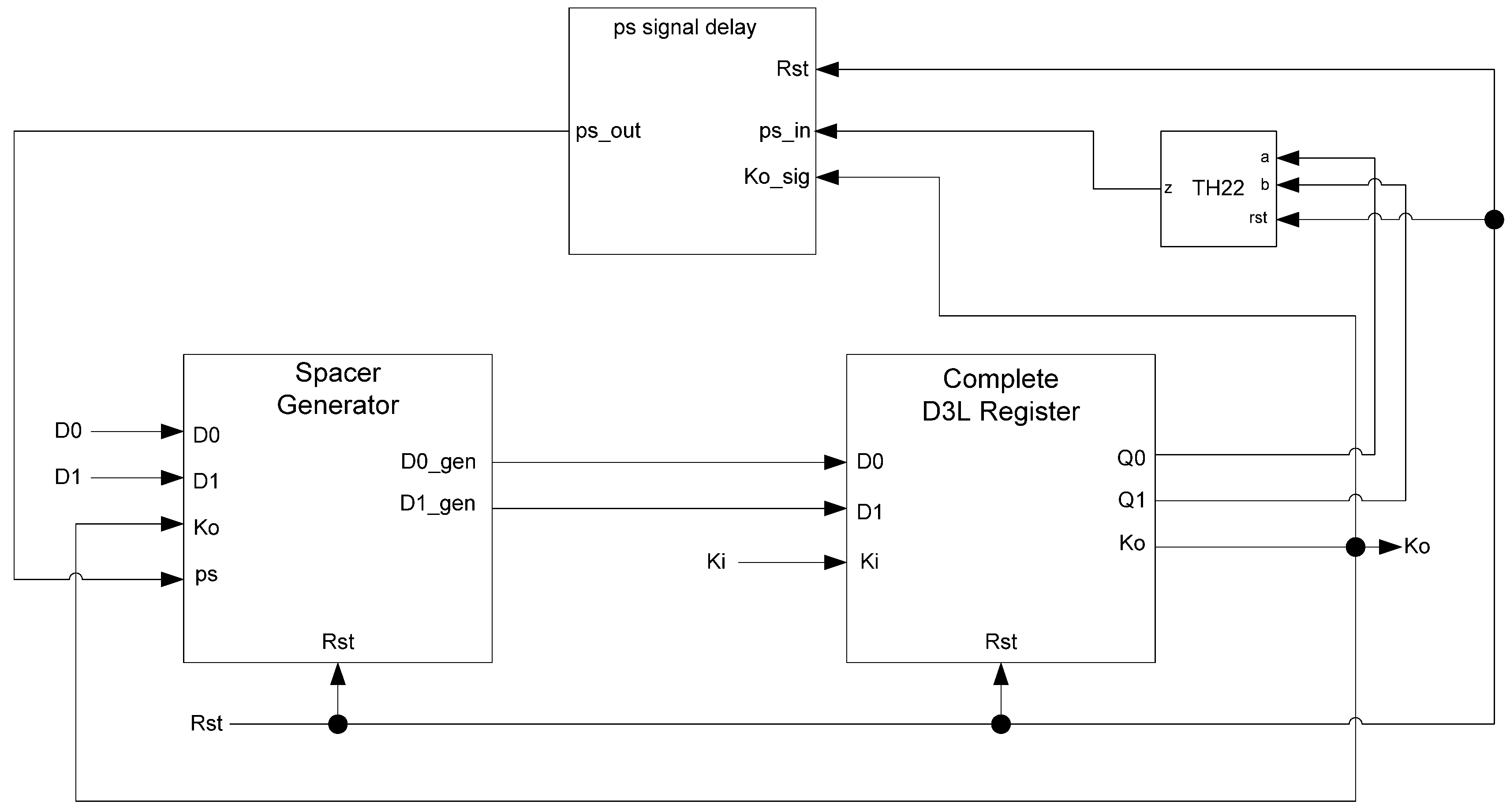
In situations where a component needs many cycles to output data but does not have input provided for each cycle, the component will not be able to receive the spacers it needs as input. Instead, a spacer generator register is used to generate these spacers for the component. A spacer generator register is a basic D3L register with a spacer generator sitting between it and its inputs. The spacer generator keeps track of the previous spacer and generates the alternate spacer when requested regardless of the dual-rail input it receives. For example, if the previous spacer was an AZS and the register requests a spacer, the spacer generator will generate an AOS. The next time a spacer is requested, it generates an AZS. Figure 17 shows the D3L spacer generator register; and Figure 18 shows the circuit diagram for the spacer generator component. The outputs of the spacer generator are given by the following equations:
D0_gen = Ko ps (D0+D1)+ Ko ps (D0+D1)+ Ko D0 D1
D1_gen = Ko ps (D0+D1)+ Ko ps (D0+D1)+ Ko D0 D1
Figure 17. D3L spacer generator register.
Jlpea 03 00300 g017
Figure 18. Spacer generator circuit diagram.
Jlpea 03 00300 g018

3. Multi-Threshold Dual-Spacer Dual-Rail Delay-Insensitive Logic (MTD3L)

3.1. Motivation

Although the D3L scheme successfully implements the dual-spacer protocol, it suffers from high overhead compared to equivalent NCL designs. This overhead comes from two sources. The first is the required NCL-X style completion logic in the form of several XNOR gates attached to each logic function. The second is the more complex registration. To eliminate the first source of overhead, the MTNCL technique can be combined with D3L, to form the new secure hardware paradigm presented in this paper, MTD3L.
Because D3L gates do not use hysteresis, an external source is required for input completion detection. Rather than using XNOR and threshold gates, the early completion technique used in MTNCL can be utilized to ensure that requests for a spacer will only be generated when all circuit inputs are that spacer and the following stage is requesting a spacer. At this point, the combinational logic can be slept to the proper value, ensuring input-completeness. Thus, the need for extra completion checking logic is eliminated.

3.2. MTD3L Gates

The addition of sleep logic to a D3L gate is simple. No modification to the D3L logic is required because it already matches the form of the modified NCL gates used in the MTNCL technique—a hold0 block and a set block. The only modification required is the addition of the sleep transistors. The sleep-to-0 transistors can be used in the same way as in SMTNCL. These transistors are responsible for the AZS transition. A similar set of transistors can be used for the AOS transition.
The sleep transistors are controlled by a pair of sleep signals, sleep-to-0 (s0) and sleep-to-1 (s1), and their complements, as shown in Table 4. These signals should not be asserted at the same time. Instead, if either of the inputs is asserted, the circuit will be slept to the appropriate value. Figure 19 shows the MTD3L gate design. When s0 is asserted, the circuit is slept to the all-zero state. In this case, the NMOS transistor parallel to the output inverter is turned on, the NMOS transistor gating the main circuit to ground is turned off, and the PMOS transistor gating the output circuit to VDD is turned off. Additionally, since s1 is off, the NMOS transistor controlled by ns1 is turned on, completing the path from the output to ground, forcing the output to logic 0. The PMOS transistor controlled by s1 is also turned on, allowing the main circuit to pass an output of 1 to the output inverter, preventing glitches from occurring when s0 is later asserted. When this happens, the output inverter will have logic 1 on its input, so it will continue to output logic 0 until new data has arrived. Similarly, when s1 is asserted, the circuit is slept to the AOS. The path to VDD for the main circuit is turned off while the path to ground remains on, allowing a 0 to eventually reach the output inverter. The output inverter’s path to ground is cut off and a direct path to VDD is formed, forcing the output to be logic 1. When the sleep-to-1 state ends, the output inverter will have logic 0 on its input so the output will remain at logic 1, preventing a glitch. If neither sleep signal is asserted, the circuit operates as it would normally. All four power- and ground-gating transistors are turned on, allowing normal access to power and ground for the circuit and output inverter. The two parallel output transistors are turned off, so the output is only controlled by the output inverter. If both sleep signals happen to be asserted at once, the four power- and ground-gating transistors will be turned off, leaving the circuit in a floating state; however, this will never occur in a properly operating circuit.
Table 4. MTD3L sleep signals.
s0s1Output
00Normal
01All-One Spacer
10All-Zero Spacer
11Invalid
Figure 19. (a) MTD3L version 1 gate structure; (b) MTD3L23 version 1 implementation.
Jlpea 03 00300 g019
One of the drawbacks of the version 1 design is the potential for very large fanouts on the sleep signals. If the design is coarsely pipelined or the combinational logic happens to be very large, a single set of sleep signals may have to drive thousands of gates, requiring these signals to be heavily buffered. Not only must s0 and s1 be buffered but their complements will require buffering as well. To mitigate this issue and reduce the number of inputs to these gates in general, a modified design may be used to eliminate the need for the complemented sleep signals, as shown in Figure 20. This design removes the power- and ground-gating transistors from the main circuit, leaving only the four transistors on the output inverter. These four transistors are controlled by s0 and the complement of s1, allowing for the removal of s0’s complement and s1 itself. Thus, only two signals must be buffered instead of four. The drawback to this technique is that the main circuit is directly exposed to power and ground, eliminating the ability to gate the circuit with high-Vt transistors.
Figure 20. (a) MTD3L version 2 gate structure; (b) MTD3L23 version 2 implementation.
Jlpea 03 00300 g020

3.3. MTD3L Registration

The basic MTD3L register, shown in Figure 21, is a modified NCL register. It consists of two TH22 gates which are resettable to the desired value. An XNOR gate facilitates early completion by checking the relative values of the register’s inputs. If both input rails have the same value then the register has received a spacer and will request data. If the values are different, then DATA has been received so the register will request the next spacer.
Figure 21. MTD3L register.
Jlpea 03 00300 g021
Additional logic is required to facilitate the dual-spacer protocol and early completion checking. The early completion component consists of resettable TH22 gates whose inputs are the register’s Ko and the next stage’s inverted Ko. The reset state of the early completion component is logic 1 if the register’s reset state is NULL and logic 0 if the register’s reset state is DATA. In order to ensure input-completeness, the early completion Ko is inverted before being passed back as the register’s Ki input. This prevents a partial spacer wavefront from passing through the register by ensuring that all of the register’s inputs are an AOS or AZS before the spacer wavefront is allowed to pass through the register. In order to facilitate the dual-spacer protocol, the same Ki Generator used in D3L registration, shown in Figure 12, is used for MTD3L.
If the register needs to supply sleep signals then sleep signal logic is used here as well, as shown in Figure 22. This logic generates two sleep signals, s0 and s1. The values of the sleep signals are shown in Table 5. If the register’s Ki is 0 then a spacer is being requested. To determine which spacer is being requested, Ki_gen’s value is used. If Ki_gen is logic 0 then an AZS is being requested; if it is logic 1 then an AOS is being requested. To avoid incorrect sleep states, a buffer is used as a delay element to ensure that the change in Ki_gen’s value is evaluated first. For example, if the desired change was from the no sleep state of row 2 to the sleep-to-1 state of row 3, then both Ki_gen and Ki will switch. If Ki switches first, a sleep-to-0 will be issued erroneously. However, if Ki_gen switches first then the no sleep state will be maintained until Ki changes as well, resulting in the correct sleep-to-1 state.
Figure 22. Complete MTD3L register.
Jlpea 03 00300 g022
Table 5. MTD3L sleep signal switching sequence.
Ki_genKis0s1
0010
0100
1001
1100
MTD3L spacer filter and spacer generator registers, shown in Figure 23 and Figure 24, respectively, are used in the same manner as they are used in D3L circuits. The filter register is used as the final register in a register ring, shown in Figure 25. It is reset to DATA and filters the spacer that passes through the ring, alternating it so that the dual-spacer protocol is enforced. The spacer generator generates the appropriate spacer as needed regardless of the values of its inputs. Typically, these registers are the ones that generate sleep signals as they are usually the registers that are facing combinational logic as shown in Figure 25. The actual spacer filter and spacer generator components are unmodified from their D3L counterparts, shown in Figure 15 and Figure 18, respectively.
Figure 23. MTD3L spacer filter register.
Jlpea 03 00300 g023
Figure 24. MTD3L spacer generator register.
Jlpea 03 00300 g024
Figure 25. MTD3L ring register.
Jlpea 03 00300 g025

4. AES Core Implementations

4.1. MTD3L Implementation

The implementation of the 128-bit AES core [46] in each design follows the same architecture. The AES transform and key expansion functions are computed in parallel. A Control block synchronizes the two functions and ensures that the correct sub-key is sent to the Transform block at the correct time. From outside, this circuit behaves as a register in terms of handshaking, so it can be easily placed into an asynchronous system. The AES core accepts an input and produces an output with one external DATA/spacer cycle. However, the AES circuit actually produces several internal DATA/spacer cycles for processing each plaintext, which are hidden from the outside. Each round of the AES algorithm consists of one of these internal cycles.
As shown in Figure 26, each design consists of five blocks: the FirstRound block, the Control block, the AESTransform block, the KeyExpansion block, and the LastRound block. The FirstRound block is a set of input registers that latch in new data and provide it to the AESTransform and KeyExpansion blocks. The AESTransform block performs the ciphertext calculation for each round of the algorithm. The KeyExpansion block calculates the subkey used in the AESTransform block. The Control block creates the control signals as well as generating the RCon constant which is used in the KeyExpansion block. The LastRound block performs the final round of calculations and also has a set of output registers to hold the final ciphertext.
Figure 26. Advanced Encryption Standard (AES) top level diagram.
Jlpea 03 00300 g026
The communication between blocks, shown in Figure 27, consists of three handshaking signals: Ki1, Ki2, and Ki3. These signals are generated by a set of threshold gates in the top level circuit. The inputs of these threshold gates are the KO values from registers throughout the design. The AESTransform, KeyExpansion, and Control blocks all have a three-ring register to save processed data. Each ring register’s Ko is used as inputs to the top-level handshaking. Additionally, an extra KO from the registers in the FirstRound and LastRound blocks is used as well. The resulting Ki1, Ki2, and Ki3 signals are used as the Ki inputs to the ring-registers mentioned previously.
Figure 27. Top level handshaking diagram.
Jlpea 03 00300 g027
The sleep signal generation mechanism consists of two types of sleep signals: a global sleep and local sleeps. The global sleep, which is a circuit input, is meant to sleep the entire circuit between encryption stages, ensuring that everything is reset properly. This sleep is only asserted after the ciphertext is latched out and external handshaking is requesting a spacer cycle. The internal sleep signals are generated locally within each block by the ring-registers. These sleeps are asserted between calculation stages. The LastRound block, lacking registration between it and the previous AESTransform block, uses the local sleep signals generated by the AESTransform block.
The FirstRound block, shown in Figure 28, consists of a set of 128-bit registers for both the input plaintext and input keys. These are regular, non-slept generating registers. The Ki to these registers is the master Ki input for the circuit. The Kos are used to generate a reset signal for the rest of the blocks, preparing them for a fresh encryption process. This reset signal also acts as the circuit’s Ko output. The data outputs of these registers go to a set of spacer-generator registers. These registers use the Ki1 signal as their Ki, synchronizing these registers with the first stage of the ring-registers throughout the design. Their Kos are not used. Next, an AddRound block calculates the initial addition of the plaintext and key, passing this data to the AESTransform block. The initial key is also passed to the AESTransform and KeyExpansion blocks. The sleep signals for the AddRound block are generated by the data processing spacer-generator register.
Figure 28. FirstRound block diagram.
Jlpea 03 00300 g028
The AES Transform block, shown in Figure 29, handles the primary calculation of the ciphertext. It consists of the main AES components: AddRound, SubByte, MixColumns, and Shiftrows. A three-ring register is used to save data between each round of calculation. To control whether the input data is taken from the FirstRound or from the circuit feedback loop, a 2-to-1 multiplexer is used. The control signal of the multiplexer is supplied by the Control block. The output of the multiplexer serves as both the output of the circuit and the feedback loop to the first register in the ring. The first and second registers are normal registers while the third is a filter register. This filter register generates the sleep signals to be used by this block as well as the subsequent LastRound block.
Figure 29. AES transform block diagram.
Jlpea 03 00300 g029
The KeyExpansion block, shown in Figure 30, is very similar to the AES Transform block. It consists of the KeyExpansion logic, a three-ring register, and a 2-to-1 multiplexer. The register and multiplexer act in the same manner as they do in the AES Transform block. The sleep signals for the KeyExpansion logic are generated by the third register in the ring, which is a filter register. The KeyExpansion logic takes the 128-bit key and transforms it into a new subkey, which is sent to the AES Transform and LastRound blocks.
Figure 30. KeyExpansion block diagram.
Jlpea 03 00300 g030
The Control block, shown in Figure 31, synchronizes all other blocks to ensure proper operation. It generates the control signals for the multiplexers throughout the design, the RCon constant used in the KeyExpansion calculations, and the control signal that activates the LastRound block. The LastRound block will only latch data to the output register when this signal is received. The input to the Control block is the reset signal generated by the Ko of the FirstRound block. This signal resets the Control block’s state, preparing it for a new encryption set.
The Control block is a state machine consisting of four components: a 5-bit three-ring register, the control signal logic, the increment logic, and the LastRound logic. The ring-register saves the state of the Control block. The filter register in this ring also generates the sleep signals for the block. The control signal logic generates the RCon signal and the multiplexer control signals. The increment logic is a counter, keeping count of the number of encryption rounds executed. When the counter reaches the round limit, the stop signal is activated.
The initial state of the Control block needs to be an AZS. However, the filter register in the ring-register is reset to data. Thus, extra logic is required to generate the initial AZS. A set of TH22n gates is used to do this. Each TH22n gate is tied to one of the signals, which is connected to both inputs of the gate. At reset, each of these gates will output a zero, giving the required spacer. Once the reset is finished, these gates will act as C-elements. Since each gate has the same signal on both inputs, its output will follow the value of the input.
Figure 31. Control block diagram.
Jlpea 03 00300 g031
The LastRound block, shown in Figure 32, consists of the final SubByte, Shiftrows, and AddRound operations on the ciphertext as well as the final output register. The MixColumns block is not used in the final round. The inputs to this block are the last transformed ciphertext from the AESTransform block and the final subkey from the KeyExpansion block. The sleep signals are the same ones generated in the AESTransform block. The register will only latch data once the stop signal is received from the Control block, which acts as the Ki to the register. This final register is a filter register, ensuring that the output from the AES circuit is capable of generating the correct spacer and sleep signals for the following circuit block.
Figure 32. LastRound block diagram.
Jlpea 03 00300 g032

4.2. AES Implementation using D3L

The D3L implementation is very similar to the MTD3L implementation. The same five blocks are used and their configurations are essentially the same. There are two primary differences between the two designs. First, since the D3L design lacks sleep signals, a global reset is used to reset the spacer-generator registers in the FirstRound between encryptions. This reset is required for the circuit to reset properly. The second major difference is the usage of completion signals. Each combinational block has a completion signal which is used to ensure input-completeness. The completion signals (ccheck) of the FirstRound and LastRound blocks are added to the Ki1 calculation. In the AES Transform block, the Ko1 output consists of the combination of the Ko from the first register as well as the ccheck signals from the multiplexer and AES logic. This is also done in the KeyExpansion and Control blocks. The ccheck signals themselves are generated with completion checking logic inside each combinational logic block.

4.3. AES Implementation using NCL

Being extensions of the NCL style, the D3L and MTD3L designs are very similar to the NCL design as well. Additionally, the NCL design served as the base of the D3L design, which was created by taking the original NCL design and replacing the gates and signals. Because of this, the structure of the blocks themselves and the combinational logic are very similar. The primary differences in the designs are found in registration, spacer generation, and input-completeness logic. Figure 33 shows the NCL AES Transform block.
NCL threshold gate logic supports input-completeness by design, so there is no need for extra input-completeness logic. Additionally, only a single register type is needed, which can be reset to the desired values. Finally, the FirstRound block, shown in Figure 34, only needs to generate NULL spacers when needed, so the spacer-generator registers are replaced with NULL generators.
Figure 33. NCL AES Transform block diagram.
Jlpea 03 00300 g033
Figure 34. NCL FirstRound block diagram.
Jlpea 03 00300 g034

4.4. AES Implementation using Synchronous Logic

The asynchronous designs are all based off the synchronous design, which was created first. Because of this, there are several similarities between the synchronous and asynchronous designs. The synchronous design, like the other designs, consists of five logic blocks. The FirstRound block is replaced with a single AddRound block. The initial register stage is instead found in the KeyExpansion and AES Transform blocks. Registers are found in the AESTransform, KeyExpansion, and Control blocks, much like the other designs. The LastRound block contains the output register which is activated with a stop signal generated by the Control block. Two designs can be used, a single clock design and a double clock design. The single clock design was used in the power and timing simulations since it is faster. The double clock design isolates the SubByte block of the AES Transform circuit in facilitating the implementation of the CPA attack. Figure 35 shows the synchronous AES Transform block.
Figure 35. Synchronous AES Transform block diagram.
Jlpea 03 00300 g035

4.5. Delay Element Design

In the D3L and MTD3L designs, a delay element was designed to help mask the relationship between the circuit delay and the data being processed. The designed delay element is a buffer chain appended to the output of the targeted Sbox that can either operate at a high speed or a low speed. The inverters that make up this chain are n-volt controlled. A second NMOS transistor is added to the pull-down network of the inverter. An example buffer is shown in Figure 36. This transistor is controlled by an external voltage. To operate at high speed, the voltage given is the same as the designated supply voltage. To operate at a slow speed, the voltage is reduced as much as possible without deforming the inverter’s output.
Figure 36. N-Volt controlled buffer.
Jlpea 03 00300 g036
To apply different voltages levels to these inverters, a control signal is generated externally. The method of generating this control signal is not important so long as the result is sufficiently random. This control signal is used to control a pair of PMOS transistors. The source of these transistors is either a high voltage source or a low voltage source. Depending on the value of the control signal, only one of these transistors will be turned on at a time, which will supply its voltage to the delay inverters. Figure 37 shows the control logic.
Figure 37. Buffer chain with voltage control.
Jlpea 03 00300 g037

5. Results and Analysis

5.1. Simulation Environment and Data Collection

Each AES design presented in Section 4 was implemented at the transistor level using Cadence and the IBM 8RF-DM 130 nm process to evaluate and compare energy consumption, speed, area, and side-channel attack resistance. The full AES designs were used for the collection of energy, speed, and area data. All simulations were done using the Cadence UltraSim simulator. Each design was simulated using the input key 0x2b7e151628aed2a6abf7158809cf4f3c.
Because a complete evaluation of the D3L and MTD3L designs requires two spacer cycles, each simulation covered two complete encryptions. For the synchronous design, the simulation begins with the circuit in its reset state. Next, the key and plaintext are given and the circuit operation continues until the ciphertext is received. On the next clock cycle, a second plaintext is entered and the second encryption cycle completes. The energy and speed of the design is calculated from the reset state until the time of completion for the second encryption. The synchronous design is controlled using vector files. The NCL, D3L, and MTD3L designs, being asynchronous, are more difficult to simulate using vector files, due to the difficulties in anticipating when the handshaking signals should be changed. Thus, the asynchronous designs are simulated using controllers defined with VerilogA, which monitors the outputs of the design and makes adjustments to the design’s inputs accordingly. The NCL simulation begins in a NULL state. The first plaintext is passed followed by another NULL state. Once this cycle completes, a second plaintext is given followed by the third NULL state. The energy and speed data is calculated from the initial state through the end of the second DATA-NULL pair. The D3L and MTD3L simulations are similar, following the pattern of AZS-DATA-AOS-DATA-AZS.
The circuit area for each design was determined by laying out each design and measuring its dimensions. First, the cell layouts were completed using the Virtuoso tool in Cadence. The full designs were placed and routed according to their respective Verilog netlists using Synopsys Astro. From there, the designs’ area could be measured. The speed of each design was simply the time it took for two encryptions to be completed and any extra time needed until a third encryption is ready to begin. The synchronous design was tested to determine its maximum clock speed. The energy consumption of each design was determined by measuring the charge of each design of the duration of the simulation period and multiplying this by the supply voltage, which was the same for each design.

5.2. Simulation Results

As shown in Table 6, the synchronous design is the fastest. The NCL design is the slowest; and the MTD3L and D3L designs are in the middle. The D3L design uses the most energy followed by the MTD3L design and the NCL design. As explained in Section 2, the D3L design suffers from significant overhead problems, which can be seen in these results, particularly with respect to energy consumption. The purpose of the MTD3L design was to reduce this overhead to more reasonable levels. In this respect, the MTD3L design has a 36% reduction in energy consumption over the D3L design. However, the MTD3L design still uses nearly 300X more energy than the synchronous design, so while some overhead reduction was achieved, more efforts are needed in order to bring the MTD3L design down to desired overhead levels.
Table 6. Speed and energy comparison.
DesignDelay (ns)Delay overhead vs. Synchronous designEnergy (nJ)Energy overhead vs. Synchronous design
Synchronous1530X1.3560X
NCL462302X2.208163X
D3L325212X6.012443X
MTD3L330216X3.84283X
Table 7 presents the area of each design after cell placement in Synopsys Astro. The MTD3L design sees significant overhead reduction compared to the D3L design. This can be attributed to the removal of the NCL_X style completion logic. With this overhead reduction, the MTD3L design is comparable to the NCL design in area.
Table 7. Area comparison.
DesignWidth (µm)Height (µm)Total Area (mm2)
Synchronous122712231.50
NCL181218093.28
D3L250325036.27
MTD3L183518383.37
The overhead of the D3L design came from two sources. The first was the NCL_X completion checking. The second was from increased registration overhead caused by the need of handling two spacers. The MTD3L design solves the first problem but does not solve the second. The reduction in MTD3L energy consumption can be attributed to the reduced completion checking overhead due to the use of early completion instead of NCL_X style checking. However, the MTD3L design still uses the same registration scheme that the D3L design uses, so this overhead remains.
Table 8 shows a comparison of the energy consumption of different components of the NCL and MTD3L designs. The energy cost of the MTD3L registration is roughly 700% greater than that of the NCL design. The combinational logic and buffering of both designs is about the same, showing that the overhead cost comes almost exclusively from the registration. Table 9 shows the differences in transistor count and average leakage of the registration for both designs, showing that the MTD3L version requires many more transistors. This is due to the logic required to implement the dual-spacer protocol, such as the Ki Generator and the Spacer Filter. These components contribute significantly to the design overhead.
Table 8. Energy comparison.
ComponentNCL design energy (nJ)MTD3L design energy (nJ)
Registration0.2521.836
Logic1.5121.26
Buffering0.4440.744
Total2.2083.84
Table 9. Registration comparison.
DesignTransistor countAverage leakage (µA)
NCL491402
MTD3L242364180

5.3. Side-Channel Attack Implementation

Because of the long simulation times required for the full designs, data collection for the power and timing attacks were performed with sub-circuits of each design. This is because each of these attacks requires many different simulation samples (256 samples in this case) to be successful. This number of simulations with the full designs would be impractical. The sub-circuits consist of the initial Addround and Subbyte stage of each design. This is because the Subbyte operation is the major vulnerable point to side-channel attacks. The attacks themselves focus on only one S-box of the Subbyte block, brute forcing all 256 plaintext input combinations of that S-box and attempting to extract one byte of the cipher key. It is assumed that if one byte of the key can be extracted then the other 15 bytes can be obtained as well.
While UltraSim in Cadence was used for the full simulations, it was found that Synopsys Nanosim could perform simulations in less time. Because so many simulation samples were required for the side-channel attacks, Nanosim was used to collect this information rather than Ultrasim. The simulation setup is similar but different for each design. For example, the synchronous design requires a clock and registers while the asynchronous designs do not. Test vectors for each design were generated. These vectors all use the same key as shown in Section 5.1. The plaintexts cover every combination of inputs for the first byte. All following bytes were kept at 0x00. Thus, the plaintexts followed the form 0xff000000000000000000000000000000. This setup helps reduce noise by attempting to isolate the attacked S-box. To help Nanosim keep track of a particular node, a small 1 ohm resistor was placed in series between the attacked S-box and its power supply.
The synchronous design consists of the Addround block and the Subbyte block with the Subbyte block being isolated by a pair of registers, as shown in Figure 38. Initially, the registers are reset to 0. Next, the key and plaintext are input to the Addround block. On the first clock edge, Addround’s output is clocked into the Subbyte block via the first register. Once the Subbyte block computes the output, the result is latched onto the second register. The second clock edge is the critical point. At this moment, the switching activity of the attacked S-box may be observed according to the changes in the second register.
Figure 38. Synchronous side-channel attack implementation.
Jlpea 03 00300 g038
As shown in Figure 39, the NCL design consists of only the Addround and Subbyte blocks. It begins the simulation in a NULL state. Next, the key and plaintext are given as DATA. After the computation is complete, a NULL wave front is input. Thus, the NCL simulation follows a NULL-DATA-NULL pattern. For the timing attack, the simulation output is divided into two sets. The first set consists of the NULL to DATA transition. The second consists of the DATA to NULL transition. Both sets have any leading and trailing zeros removed to help align and simply the data for the timing attack.
The D3L and MTD3L designs also consist only of Addround and Subbyte blocks. Like the NCL simulation, these designs begin at the AZS. The plaintext and key are input as DATA. Once the circuit is finished, an AOS is given next. The same plaintext and key are input as DATA a second time. Once the second computation is complete, another AZS is given. Thus, these designs follow a complete dual-spacer pattern of AZS-DATA-AOS-DATA-AZS. The same data is given twice to help simplify the power and timing attacks. These data sets are divided into four groups for the timing attack. The first is the transition from the AZS to DATA. The second is the transition from DATA to the AOS. The third is from the AOS to DATA. The last is from DATA to the AZS. Each set has leading and trailing zeros removed much like the NCL data.
Figure 39. NCL, D3L, and MTD3L side-channel attack implementation.
Jlpea 03 00300 g039
The D3L and MTD3L designs were also tested with the random delay elements, presented in Section 4, inserted into the targeted S-box, as shown in Figure 40. These delay elements are attached to each of the outputs of the target S-box. They are controlled by a signal generated by the bitwise XOR of the outputs of the Addround Z1 rail. The simulation setup is otherwise the same as the previous D3L and MTD3L simulations.
Figure 40. D3L and MTD3L delayed side-channel attack implementation.
Jlpea 03 00300 g040
The power and timing attacks were carried out with a Java program. The program takes the simulation data and a statistical model of the design as input. The format of the simulation data depends on the type of attack being done. For the synchronous design, the only attack was a power analysis attack. The simulation input was in the form of a set of values of the current drawn by the power supply at a given time. The statistical model was the calculated Hamming distance given the key guess and the given plaintext. The NCL design was attacked using an energy based model. The simulation data began as a set of current values, similar to the synchronous data. This data was summed over the duration of the simulation period resulting in a single value representing the energy used in the simulation. The D3L and MTD3L designs were also attacked with an energy based model. In addition to this attack, the D3L and MTD3L designs were also attacked with a timing model. Similar to the energy attack, the power data was converted to a single time value by measuring the number of time steps where the circuit was drawing power. It is assumed that the circuit only draws significant current while it is calculating the ciphertext. The total number of discrete time steps above this threshold represent the time it took to complete the operation. Because the asynchronous designs are designed to balance switching activity independently of the data given, the Hamming distance model used for the synchronous attack is not sufficient for the asynchronous attacks. Instead, the expected energy and timing of these designs was estimated by counting the expected number of transistor switches for a given input combination. It is assumed that the energy and time delay of the circuit for a given set of inputs is directly proportional to the number of transistors that switch as a result of those inputs. The energy attacks were carried out over the complete simulation data. The timing attacks were carried out over the partitioned data.

5.4. Side-Channel Attack Results

Table 10 shows the results of the power- and energy-based attacks. The highest correlation out of the set of key guesses is shown for each design as if the highest correlation guess was generated by the correct key value. For the timing attacks against the asynchronous designs, which were each partitioned into several parts, only the part that resulted in the highest correlation is given. For example, the MTD3L timing attack had the highest result for the first data to AOS transition, so only that result is given. All other MTD3L transitions resulted in lower correlations. The synchronous attack was successful while the NCL, D3L and MTD3L attacks were not. The synchronous design, having no defense against power analysis, resulted in the highest correlation coefficient. This means that the key guess for this design has the most confidence. The NCL, D3L, and MTD3L designs each resulted in a lower coefficient and failure to guess the correct key. The D3L and MTD3L coefficients were very similar. This is expected because the changes from the D3L design to the MTD3L design should not have impacted the MTD3L design’s side-channel defenses. The NCL coefficient was unexpectedly the lowest, in disagreement with the results from [41], where the key was correctly guessed for the NCL circuit implemented using the IBM 0.5 μm process. This could be due to a number of reasons, such as a weakness in the statistical model, lack of resolution in the simulation data, or the unbalanced load effect in NCL being somewhat amplified in the large non-digital 0.5 μm process.
Table 10. Power/energy attack results.
DesignAttack typeCorrelation coefficientCorrect key guess success/failure
SynchronousPower0.872Success
NCLEnergy0.207Failure
D3LEnergy0.376Failure
MTD3LEnergy0.353Failure
Table 11 shows the results of the time based attacks. The synchronous design was not attacked in this way, since it is already known to be susceptible, while the NCL design, also known to be susceptible, was attacked to show that the attack algorithm being used for the asynchronous designs could correctly guess the key. Since the energy attack on the NCL circuit in [41] was successful, adding random delay elements to protect it from timing attacks was moot, so this was not done. For the D3L and MTD3L circuits, only a minimal number of random delay elements were added to reduce the correlation coefficient, since reducing area without compromising susceptibility is the main objective. None of the attacks against the D3L or MTD3L designs were successful; the correlations for these designs were very similar and quite low, showing weak correlation between the statistical models and the actual behavior of the designs. Adding random delay elements is not necessary to further protect the D3L and MTD3L circuits against timing attacks, since this had minimal impact on reducing their correlation coefficients. Again, the MTD3L design performed very similarly to the D3L design. These results as well as the results given in Section 5.2 show that the MTD3L design offers similar security to the D3L design while having much less overhead with regard to area and power consumption.
Table 11. Timing attack results.
DesignCorrelation coefficientCorrect key guess success/failure
NCL0.400Success
D3L0.337Failure
MTD3L0.366Failure
Delayed D3L0.326Failure
Delayed MTD3L0.367Failure

6. Conclusions and Future Work

This paper develops MTD3L, an enhancement to the D3L technique presented in [41], by combining D3L with MTNCL. Because the D3L technique suffered significant overhead with respect to area and power consumption, a method of reducing overhead to make D3L more reasonable was necessary. The resulting MTD3L method shows significant reductions in power consumption and area overhead, and demonstrated the same strength as the D3L technique against power and timing analysis attacks. The end result is that the MTD3L technique is a substantial improvement over the original D3L technique, and is applicable for designs where security is much more important than power consumption or area, since MTD3L still has significant overhead compared to the original synchronous design. Hence, more work is required to reduce the overhead even further.
The majority of the overhead is from the increased complexity of the registration stage. This complexity was also present in the original D3L technique. The overhead required to implement the dual-spacer protocol, particularly in the filter registers, makes D3L and MTD3L registers much larger and consume much more power than NCL or synchronous registers. Therefore, course-grained pipelines will have much less overhead than fine-grained ones. Future work includes investigations of possible ways to reduce this registration overhead, bringing the MTD3L implementation cost closer to that of the NCL design.
Note that although complete layouts of the circuits were done, including place and route, all simulations were performed on the transistor-level circuits. This was because post-parasitic extraction simulations consumed all of the server memory and caused the system to crash. Since both power and timing attacks are strongly correlated to circuit parasitics, the authors have been actively applying for funding to fabricate these circuits so that hardware measurements can be made.

Conflicts of Interest

The authors declare no conflict of interest.

References

  1. Jaffe, J.; Kocher, P.; Jun, B. Differential Power Analysis. In Proceedings of 19th International Advances in Cryptology Conference, Santa Barbara, CA, USA, 16–20 August 2009; pp. 388–397.
  2. Brier, E.; Clavier, C.; Olivier, F. Correlation Power Analysis with a Leakage Model. In Proceedings of Cryptographic Hardware and Embedded Systems (CHES) 2004, Cambridge, MA, USA, 11–13 August 2004; pp. 16–29.
  3. Blake, I.; Seroussi, G.; Smart, N.; Cassels, J.W.S. Advances in Elliptic Curve Cryptography; Cambridge University Press: New York, NY, USA, 2005. [Google Scholar]
  4. Messerges, T.; Dabbish, E.; Sloan, R. Investigations of Power Analysis Attacks on Smartcards. In Proceedings of Workshop on Smartcard Technology, McCormick Place South Chicago, IL, USA, 10–11 May 1999; p. 17.
  5. Coron, J. Resistance against Differential Power Analysis for Elliptic Curve Cryptosystems. In Proceedings of 1st International Workshop on Cryptographic Hardware and Embedded Systems, Worcester, MA, USA, 12–13 August 1999; pp. 292–302.
  6. Boer, B.; Lemke, K.; Wicke, G. A DPA Attack against the Modular Reduction within a CRT Implementation of RSA. In Proceedings of 4th International Workshop on Cryptographic Hardware and Embedded Systems, Redwood Shores, CA, USA, 13–15 August 2002; pp. 228–243.
  7. Serner, S.; Colin, W. More Detail for a Combined Timing and Power Attack against Implementations of RSA. In Proceedings of the Institute of Mathematics and its Applications (IMA) International Conference, Cirencester, UK, 16–18 December 2003; pp. 245–263.
  8. Ors, S.; Gurkaynak, F.; Oswald, E.; Preneel, B. Power-Analysis Attack on an ASIC AES implementation. In Proceedings of International Conference on Information Technology: Coding and Computing, The Orleans, NV, USA, 5–7 April 2004; pp. 546–552.
  9. Boracchi, G. A Study on the Efficiency of Differential Power Analysis on AES S-Box; Technical Report, Elettronica e Informazione, Politecnico di Milano: Milano, Italy, 2007. [Google Scholar]
  10. Chari, S.; Jutla, C.; Rao, J.; Rohatgi, P. A Cautionary Note Regarding Evaluation of AES Candidates on Smart Cards. In Proceedings of 2nd Advanced Encryption Standard Candidate Conference, Rome, Italy, 22–23 March 1999; pp. 133–147.
  11. Berna, O.; Elisabeth, O.; Bart, P. Power-Analysis Attacks on an FPGA—First Experimental Results. In Proceedings of 5th International Workshop on Cryptographic Hardware and Embedded Systems (CHES), Cologne, Germany, 8–10 September 2003; pp. 35–50.
  12. Ors, S.; Gurkaynak, F.; Oswald, E.; Preneel, B. Power-Analysis Attack on an ASIC AES Implementation. In Proceedings of International Conference on Information Technology: Coding and Computing, Las Vegas, Nevada, USA, 5–7 April 2004; pp. 546–552.
  13. Mace, F.; Standaert, F.; Quisquater, J.; Legat, J. A Design Methodology for Secured ICs Using Dynamic Current Mode Logic. In Proceedings of 15th International Workshop on Integrated Circuit and System Design, Power and Timing Modeling, Optimization and Simulation (PATMOS), Leuven, Belgium, 21–23 September 2005; pp. 550–560.
  14. Verbauwhede, I.; Tiri, K.; Hwang, D.; Schaumont, P. Circuits and Design Techniques for Secure ICs Resistant to Sidechannel Attacks. In Proceedings of IEEE International Conference on Integrated Circuit Design and Technology (ICICDT), Padova, Italy, 24–26 May 2006.
  15. Aigner, M.; Mangard, S.; Menicocci, R.; Olivieri, M.; Scotti, G.; Trifiletti, A. A Novel CMOS Logic Style with Data Independent Power Consumption. In Proceedings of International Symposium on Circuits and Systems, Kobe, Japan, 23–26 May 2005; pp. 1066–1069.
  16. Lin, K.; Fan, S.; Yang, S.; Lo, C. Overcoming Glitches and Dissipation Timing Skews in Design of DPA Resistant Cryptographic Hardware. In Proceedings of Design, Automation & Test in Europe Conference & Exhibition, Nice, France, 16–20 April 2007; pp. 1265–1270.
  17. Sundaresan, V.; Rammohan, S.; Vemuri, R. Power Invariant Secure IC Design Methodology Using Reduced Complementary Dynamic and Differential Logic. In Proceedings of IFIP International Conference on Very Large Scale Integration and System-on-Chip (VLSI-SoC), Atlanta, USA, 15–17 October 2007; pp. 1–6.
  18. Kulikowski, K.; Venkataraman, V.; Wang, Z.; Taubin, A. Power Balanced Gates Insensitive to Routing Capacitance Mismatch. In Proceedings of Design, Automation & Test in Europe Conference & Exhibition, Munich, Germany, 10–14 March 2008; pp. 1280–1285.
  19. Wang, Y.; Leiwo, J.; Srikanthan, T.; Jianwen, L. An Efficient Algorithm for DPA-resistant RSA. In Proceedings of IEEE Asia Pacific Conference on Circuits and Systems (APCCAS), Singapore, 4–7 December 2006; pp. 1659–1662.
  20. Mesquita, D.; Techer, J.; Torres, L.; Sassatelli, G.; Cambon, G.; Robert, M.; Moraes, F. Current Mask Generation—A Transistor Level Security Against DPA Attacks. In Proceedings of 18th Symposium on Integrated Circuits and Systems Design, Florianolpolis, Brazil, 4–7 September 2005; pp. 115–120.
  21. Haider, S.; Nazhandali, L. Utilizing Sub-threshold Technology for the Creation of Secure Circuits. In Proceedings of International Symposium on Circuits and Systems (ISCAS), Seattle, WA, USA, 18–21 May 2008; pp. 3182–3185.
  22. Hasan, M. Power analysis attacks and algorithmic approaches to their countermeasures for koblitz curve cryptosystems. IEEE Trans. Comput. 2001, 50, 1071–1083. [Google Scholar] [CrossRef]
  23. Corsonello, P.; Perri, S.; Margala, M. An Integrated Countermeasure against Differential Power Analysis for Secure Smart-Cards. In Proceedings of International Symposium on Circuits and Systems (ISCAS), Island of Kos, Greece, 21–24 May 2006; pp. 5611–5614.
  24. Yang, S.; Wolf, W.; Vijaykrishnan, N.; Serpanos, D.; Xie, Y. Power Attack Resistant Cryptosystem Design—A Dynamic Voltage and Frequency Switching Approach. In Proceedings of Design, Automation & Test in Europe Conference & Exhibition, Munich, Germany, 7–11 March 2005; pp. 64–69.
  25. Baddam, K.; Zwolinski, M. Evaluation of Dynamic Voltage and Frequency Scaling as a Differential Power Analysis Countermeasure. In Proceedings of 20th International Conference on VLSI Design held jointly with 6th International Conference on Embedded Systems, Bangalore, India, 6–10 January 2007; pp. 854–862.
  26. Ambrose, J.; Ragel, R.; Parameswaran, S. RIJID—Random Code Injection to Mask Power Analysis based Side Channel Attacks. In Proceedings of Design Automation Conference (DAC), Yokohama, Japan, 23–26 January 2007; pp. 489–492.
  27. Rivain, M.; Dottax, E.; Prouff, E. Block Ciphers Implementations Provably Secure Against Second Order Side Channel Analysis. In Proceedings of Fast Software Encryption, Lausanne, Switzerland, 10–13 February 2008.
  28. Kocher, P.C. Timing Attacks on Implementations of Diffie-Hellman, RSA, DSS, and Other Systems. In Proceedings of 16th International Advances in Cryptology Conference, Santa Barbara, CA, USA, 20–24 August 2006; pp. 388–397.
  29. Chevallier-Mames, B.; Ciet, M.; Joye, M. Low-cost solutions for preventing simple side-channel analysis—Side-channel atomicity. IEEE Trans. Comput. 2004, 53, 760–768. [Google Scholar] [CrossRef]
  30. Page, D.; Smart, N. Parallel cryptographic arithmetic using a redundant montgomery representation. IEEE Trans. Comput. 2004, 53, 1474–1482. [Google Scholar] [CrossRef]
  31. Hodjat, A.; Hwang, D.; Verbauwhede, I. A Scalable and High Performance Elliptic Curve Processor with Resistance to Timing Attacks. In Proceedings of International Conference on Information Technology: Coding and Computing, Las Vegas, USA, 4–6 April 2005; pp. 538–543.
  32. Sokolov, D.; Murphy, J.; Bystrov, A.; Yakovlev, A. Design and analysis of dual-rail circuits of security applications. IEEE Trans. Comput. 2005, 54, 449–460. [Google Scholar] [CrossRef]
  33. Bouesse, G.; Renaudin, M.; Dumont, S.; Germain, F. DPA on Quasi Delay Insensitive Asynchronous Circuits— Formalization and Improvement. In Proceedings of Design, Automation & Test in Europe Conference & Exhibition, Munich, Germany, 7–11 March 2005; pp. 424–429.
  34. Verbauwhede, I.; Tiri, K.; Hwang, D.; Schaumont, P. Circuits and Design Techniques for Secure ICs Resistant to Sidechannel Attacks. In Proceedings of IEEE International Conference on Integrated Circuit Design and Technology (ICICDT), Padova, Italy, 24–26 May 2006.
  35. Shang, D.; Burns, F.; Bystrov, A.; Koelmans, A.; Sokolov, D.; Yakovlev, A. High-security asynchronous circuit implementation of AES. IEE Proc. Comput. Digit. Tech. 2006, 153, 71–77. [Google Scholar] [CrossRef]
  36. Kulikowski, K.; Venkataraman, V.; Wang, Z.; Taubin, A.; Karpovsky, M. Asynchronous Balanced Gates Tolerant to Interconnect Variability. In Proceedings of International Symposium on Circuits and Systems (ISCAS), Seattle, WA, USA, 18–21 May 2008; pp. 3190–3193.
  37. Baddam, K.; Zwolinski, M. Path switching: A technique to tolerate dual rail routing imbalances. Des. Autom. Embed. Syst. 2008, 12, 207–220. [Google Scholar]
  38. Fant, K.; Brandt, S. NULL Convention Logic™: A Complete and Consistent Logic for Asynchronous Digital Circuit Synthesis. In Proceedings of Application Specific Systems, Architectures and Processors, Chicago, IL, USA, 19–23 August 1996; pp. 261–273.
  39. Di, J.; Yang, F. D3L—A Framework on Fighting Against Non-Invasive Attacks to Integrated Circuits for Security Applications. In Proceedings of 3rd IASTED International Conference Circuits, Signals and Systems, Marina del Rey, CA, USA, 24–26 October 2005; pp. 73–78.
  40. Wu, J.; Kim, Y.; Choi, M. Low-Power Side-Channel Attack-Resistant Asynchronous S-Box Design for AES Cryptosystems. In Proceedings of Great Lakes Symposium on VLSI (GLSVLSI), Providence, RI, USA, 16–18 May 2010; pp. 459–464.
  41. Cilio, W.; Di, J.; Smith, S.C.; Thompson, D.R. Mitigating Power- and Timing-Based Side-Channel Attacks Using Dual-Spacer Dual-Rail Delay-Insensitive Asynchronous Logic. Microelectron. J. 2013, 44, 258–269. [Google Scholar] [CrossRef]
  42. Di, J.; Smith, S.C. Ultra-Low Power Multi-Threshold Asynchronous Circuit Design. U.S. Patent 7,977,972 B2, 12 July 2011. [Google Scholar]
  43. Smith, S.C.; Di, J. Designing Asynchronous Circuits Using NULL Convention Logic (NCL); Synthesis Lectures on Digital Circuits and Systems, Morgan & Claypool: Oak View Drive San Rafael, CA, USA, July 2009. [Google Scholar]
  44. Muller, D.E. Asynchronous Logics and Application to Information Processing. In Switching Theory in Space Technology; Stanford University Press: St. Redwood, CA, USA, 1963; pp. 289–297. [Google Scholar]
  45. Kondratyev, A.; Lwin, K. Design of asynchronous circuits using synchronous CAD tools. J. IEEE Des. Test 2002, 19, 107–117. [Google Scholar] [CrossRef]
  46. National Institute of Standards and Technology, Federal Information Processing Standard 197, the Advanced Encryption Standard (AES). Available online: http://csrc.nist.gov/publications/fips/fips197/fips-197.pdf (accessed on 20 October 2013).

