SU-8 Photolithography as a Toolbox for Carbon MEMS


Mechanical Engineering Department, Clemson University, 250 Fluor Daniel, Clemson, SC 29634, USA
Micromachines 2014, 5(3), 766-782; https://doi.org/10.3390/mi5030766
Submission received: 26 June 2014
/
Revised: 4 September 2014
/
Accepted: 9 September 2014
/
Published: 22 September 2014
(This article belongs to the Special Issue 15 Years of SU8 as MEMS Material)
Abstract
:The use of SU-8 as precursor for glass-like carbon, or glassy carbon, is presented here. SU-8 carbonizes when subject to high temperature under inert atmosphere. Although epoxy-based precursors can be patterned in a variety of ways, photolithography is chosen due to its resolution and reproducibility. Here, a number of improvements to traditional photolithography are introduced to increase the versatility of the process. The shrinkage of SU-8 during carbonization is then detailed as one of the guidelines necessary to design carbon patterns. A couple of applications—(1) carbon-electrode dielectrophoresis for bioparticle manipulation; and (2) the use of carbon structures as micro-molds are also presented.

1. Introduction
The focus of the work presented here is the derivation of glass-like carbon microstructures from SU-8, an epoxy-based photoresist. Carbon MEMS (microelectro mechanical systems) (or C-MEMS) can be defined as the set of methods that can be used to derive glass-like carbon structures from patterned organic polymers, featuring dimensions ranging from hundreds of micrometers down to tens of nanometers. Carbon MEMS combines different micro- and nano-fabrication techniques with pyrolysis to derive glass-like carbon features. These fabrication techniques include stamping, casting, machining and lithography; the choice between them is dictated by the quality, complexity and final dimensions of the desired carbon part. Photolithography, or patterning with light, is emphasized here. The incorporation of SU-8 photolithography to the carbon MEMS toolbox enables exquisite control on the dimensions and complexity of the precursor polymer structures. The existence of a commercial high-quality SU-8 formulation and standardized photolithography tools makes the fabrication process and the dimensional control highly reproducible.
Glass-like carbons are derived through the pyrolysis, or thermal degradation, of organic polymers in inert atmospheres. The name, glass-like carbon, comes from the fact that carbon resulting from pyrolysis has a glass-like appearance in the sense that is smooth, shiny and exhibits a conchoidal fracture. Glass-like carbon is a carbon allotrope with very high isotropy of its structural and physical properties and with a very low permeability for liquids and gases. Up to now, a consensus on its crystalline structure has not been reached, but the most widely known and accepted model considers it to be made up of tangled and wrinkled aromatic ribbon molecules randomly cross-linked by carbon-carbon covalent bonds [1,2]. Such a structure reflects the structural features of thermosetting resins, commonly used as carbon precursors. Furthermore, this model so far explains most of characteristics experimentally determined on glass-like carbons, including its impermeability, brittleness and conductivity [1,2,3,4]. It is important to note that although its structure is amorphous, glass-like carbon cannot be correctly referred to as amorphous carbon, since such a term is now restricted by the International Union of Pure and Applied Physics (IUPAC) to the description of carbon materials with localized π-electrons [5]. Even if coal, soot, carbon black and glass-like carbons are informally called amorphous carbon, they are products of pyrolysis, which does not produce true amorphous carbon under normal conditions.
Glass-like carbon is impermeable to gases and extremely inert, with a remarkable resistance to chemical attack from strong acids, such as sulfuric and hydrofluoric, and other corrosive agents, such as bromine. It can be etched at high temperatures under oxygen atmosphere, but its rate of oxidation in oxygen, carbon dioxide or water vapor is lower than those of any other carbon. It also has a wider electrochemical stability window than platinum and gold, which makes it ideal in electrochemistry experiments [6,7]. Regarding its mechanical properties, its Young’s modulus ranges between 10 and 40 GPa and features a hardness of 6 to 7 on Mohs’ scale, a value comparable to that of quartz. Its density value falls between 1.4 and 1.5 g/cm3 [8], compared to 2.3 g/cm3 for graphite, hence suggesting a significant degree of porosity. X-ray diffraction studies have shown that glass-like carbon presents an extremely small pore size, around 50 Å, of a closed nature [9,10]. Glass-like carbon features a coefficient of thermal expansion of 2.2–3.2 × 10⁻⁶/K, similar to some borosilicate glasses. Because its thermal conductivity is about a tenth of the value for typical graphite, it has been considered as thermally inert. Its electric and electronic properties have been recently reviewed by other authors [2,11,12,13,14]. Naturally, the exact properties of the resulting carbon depend on the nature of the precursor used, but they do not change very significantly [3], and the above values could be employed as an initial reference for most precursors, including SU-8.
Developed by scientists at IBM and patented as far back as 1989 [15], SU-8 is an acid-catalyzed negative photoresist, made by dissolving a bisphenol-A novolac resin (EPON® SU-8 resin, a registered trademark of Shell Chemical Company, The Hague, The Netherlands) in an organic solvent, such as cyclopentanone or GBL (gamma-butyrolactone), and adding up to 10% in weight of a photoinitiator, usually triarylsulfonium hexafluoroantimonate. The viscosity of the photoresist and, hence, the range of thicknesses accessible are determined by the ratio of solvent to resin. The EPON resist is a multifunctional, highly-branched epoxy derivative that consists of bisphenol—A novolac glycidyl ether. On average, a single molecule contains eight epoxy groups, which explains the eight in the name, SU-8. In a chemically-amplified resist, like SU-8, one photon produces a photoproduct that, in turn, causes hundreds of reactions that together change the solubility of the film. Because of its aromatic functionality and highly cross-linked matrix, the SU-8 resist is thermally stable and chemically very inert. The low molecular weight (~7000 ± 1000 Da) and multifunctional nature of the epoxy give it a high cross-linking propensity, which also reduces the solvent-induced swelling typically associated with negative resists. As a result, a very fine feature resolution can be obtained. Low molecular weight characteristics also translate into high contrast and high solubility; and because of its high solubility, very concentrated resist casting formulations can be prepared. Such an increased concentration benefits thick film deposition, up to 500 µm in one coat, and planarization of extreme topographies. SU-8 photoresists are currently commercially available through MicroChem Corporation (Newton, MA, USA) and Gersteltec Sárl (Pully, Switzerland).
Photolithography is patterning with light. The material to be patterned, a photoresist, changes its chemical composition upon being exposed to light of specific wavelengths (usually 365 nm, the i-line, or 436 nm, the g-line). In SU-8, light starts a cross-linking reaction in the matrix, making the exposed section less soluble in a developer. Masks, a patterned stencil that enables the selective passage of light, must then be designed according to the desired final topography: transparent areas in the mask must correspond to the topography to be fabricated. In 2002, the derivation of carbon films from SU-8 was first reported by Singh and colleagues [16]. In 2005, structures with aspect ratios higher than 10 were reported by Wang et al. [17], and since then, a variety of complex carbon microstructures have been derived from SU-8. The fabrication of high-aspect ratio structures [18,19], nano-electrodes [20], free-standing all-carbon micromolds [21,22], wires [23] and the integration of carbon electrodes in polymer devices for particle manipulation [24] are included in the latest achieved milestones. Here, I first present a number of possible optimization steps in a traditional SU-8 photolithography process that can lead to innovative carbon structures. Secondly, an overview of the carbonization process and results obtained with SU-8 are presented. At last, two applications, carbon-electrode dielectrophoresis and carbon micromolds, developed by this author and his collaborators, are summarized.
2. Photolithography of SU-8
Photolithography generally involves a set of basic processing steps: photoresist deposition on a substrate, a soft bake to evaporate the solvent, exposure to initiate cross-linking, a post-exposure bake to finalize cross-linking and developing to obtain the exposed topography. Cross-linking of the photoresist depends on the combination of exposure dose (time and energy) and post-exposure bake time and temperature. If the topography to be fabricated is a dense array of small features, the use of low exposure dose and increased post-exposure bake is recommended. The contrary is recommended when features with a wide footprint are desired, since increased baking times or temperatures can introduce stress in the matrix and lead to cracking and feature lift-off during development. The basics of SU-8 photolithography have been previously covered by a number of authors [25,26], including the current one [27], and are out of the scope of this work. Instead, here, I briefly present a number of possible improvements in different stages of the photolithography process to increase its versatility. Some of these improvements enabled the applications presented in Section 4.
2.1. Releasable Substrate for Free-Standing Parts
The first refinement to a traditional photolithography process is the replacement of the rigid substrate, like silicon, by a flexible substrate. After photolithography, such a flexible film can be peeled away to yield free-standing SU-8 structures. These structures can then be carbonized and used as carbon micromolds, as will be detailed in Section 4.2. Previous approaches for the fabrication of free-standing structures traditionally used rigid substrates coated with a layer of sacrificial material, for example dry film photoresist or positive photoresists [28]. SU-8 is photopatterned on top of such a sacrificial material and the topography released by chemically dissolving the sacrificial layer with the proper solvent, which can be water. This final release, however, tends to be lengthy, given the thin nature of the sacrificial layer; and it gets lengthier as the footprint of the SU-8 structure increases. The use of flexible substrates would allow for the easy and quick peeling of the substrate immediately after the developing step; and no chemical baths would be required.
The process about to be presented is detailed elsewhere [21]. Briefly, the first step in the process was to fasten polymer films to an aluminum ring, 1.78 mm-thick, in a manner similar to a membrane being fitted to a drum (see the Supplementary, Figure S1). Two flexible films were tested as substrates: 127 μm-thick Kapton® and 70-μm Mylar®. The film was fastened to the aluminum ring, 4″ in diameter, until it was flat and tense, to provide a planar surface and to facilitate the spin coating of the resist. The photolithography process was then conducted as per the processing guidelines of the SU-8 manufacturer, taking care not to heat the arrangement above the glass transition temperature of the flexible substrate. After the photolithography process, the film containing the SU-8 topography is unfastened from the aluminum ring and bent throughout to release the SU-8 structures (see the Supplementary, Figure S2). Only the use of Mylar led to an easy and clean release of the SU-8 structures, due to the poor adhesion between them. The adhesion of SU-8 to Kapton is strong enough to cause breakage of the SU-8 structures. Additionally, Kapton significantly absorbs UV-light and, thus, renders backexposure (see Section 2.3) of the resist impossible. However, Mylar film should only be released after the developing step and not prior. Attempts to remove it prior to development resulted in mechanical deformation of the part, as the adhesion of un-crosslinked SU-8 is significantly higher than that of its cross-linked version.
2.2. Dense Arrays of High Aspect Ratio Structures
SU-8 is an ideal candidate to fabricate high aspect ratio structures for a number of applications; for example, in the fabrication of lateral flow arrays, where an array of structures is functionalized to act as a sensor in biomedical diagnostics, as molds in soft lithography or as precursors of glass-like carbon electrode arrays to be used in carbon-electrode dielectrophoresis, as detailed in Section 4.1. In any case, one is looking for arrays of tall structures with narrow gaps, usually below 30 µm, in between them. To achieve this, a few general considerations in SU-8 processing must be taken into account. First, even though SU-8 allows for coating of layers up to 500 µm in one step, layers that are so thick often lack surface uniformity; the surface can be wavy with thickness variations in the tens of micrometers. Such random variation will negatively impact the photolithography process during the exposure step, when the distance between the mask and the resist is supposed to be uniform throughout, by allowing for air gaps between the resist and the mask. These gaps enable light to diffract at the film-mask interface and can lead to the broadening of the structures at the top, a well-known effect commonly known as T-topping [26,29,30]. For example, when exposing thick layers (>200 µm) coated in a single step, it was common to find T-topped features in one area of the wafer, while they are perfectly fine in other ones, even though the exposure and post-baking times were the same. T-topping is a significant problem, disabling indeed, when fabricating dense arrays of features, since it can lead to the joining of the structures at their top. Different exposure contact modes are available in photolithography: proximity, where the distance between the mask and resist can be set to a specific value; soft contact, where the resist is barely brought into contact with the mask; and hard contact, where the resist is pushed against the mask with the purpose of eliminating any air gaps in between them. The exposure of dense arrays of features greatly benefits from using the hard contact mode, since the resist is pressed against the mask, and air gaps throughout the exposure area are minimized. Alternatively, one may use an index matched material to fill the air gaps; glycerol for example [30]. Yet another way to eliminate air gaps is a multi-step coating process for layers above 100 µm thick. The most viscous formulations commercially available, SU-8 2150 and GM1075, feature good surface uniformity only below 100 µm (data not shown), and coatings in thickness steps of 100 µm or less are recommended.
Second, the exposure dose used for dense arrays should be less than that recommended in the processing datasheet for a specific layer thickness. Lower doses minimize the chance of starting a cross-linking reaction in the narrow gaps between high aspect ratio structures due to light diffraction. A recommended initial value based on this author’s work is 180 mJ/cm2 for layer thicknesses up to 200 µm followed by a 60-min post-exposure bake at 95 °C [31]. Note that the baking time is increased with respect to that recommended in the datasheet to ensure complete cross-linking.
Third, just using a different mask, an important advantage of photolithography over other techniques, can easily change the cross-section of the structures. The choice of cross-section can lead to more stable structures by optimizing their moment of inertia. This plays an important role when fabricating tall structures with narrow gaps in between them, as stiction forces during drying can cause their collapse. The surface tension forces that develop in a narrow gap during the drying of these patterns from developer fluid can pull the structures together. Increasing the stiffness of the individual structures can minimize stiction; as well as increasing the gap between them or using a developer with a low surface tension. The stiffness of a structure mainly depends on the Young’s modulus, around 4 GPa for SU-8, its dimensions and geometry. A detailed analysis on the stiction force depending on the structure properties, the gap between them and the developer fluid is presented elsewhere [32]. In general, circular pillars with an aspect ratio less than four, a height below 400 µm and gaps as narrow as 15 µm are easily fabricated when using isopropyl alcohol to replace the SU-8 developer before manual drying using a nitrogen gun. Narrower gaps between taller and slimmer structures may require the use of critical point drying.
2.3. Backexposure for Tapered Structures
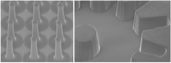
Traditional photolithography uses optimized top exposure of the SU-8 film to achieve straight walls in high aspect ratio structures. If the film is underexposed, the walls will no longer be straight, but feature a V-profile [33]. Following the same rationale, tapered structures can be made in SU-8 if the layer is underexposed, but through the substrate. These SU-8 structures can lead to tapered carbon electrodes for various applications; to puncture through tissue, for instance, and to obtain a better electrical signal. Preliminary results show how the shape and dimensions of the tapered structure can be tailored by varying the exposure dose and the post-exposure baking time. The exposure dose determines the shape and height of the carbon cone, while an optimized post-exposure baking time is needed to finalize the cross-linking of a given shape. If the post-exposure bake is not long enough, the partially-exposed features will be washed away during developing. This initial study started by spin coating a 100 µm-thick SU-8 layer (GM1075, Gersteltec, Pully, Switzerland) on a fused silica substrate and soft baking it at 120 °C for one hour. The layer was then exposed through the transparent substrate with different doses, 50 to 190 mJ/cm2 in steps of 20, using an i-line UV source. All features were baked after exposure for the same time (one hour) and temperature (95 °C). Results are shown in Figure 1 after all SU-8 precursor structures were carbonized following the exact same protocol. Low exposure doses led to short, flattened cones on the substrate (Figure 1a), since the layer is only minimally exposed. As the dose increases, the cones start increasing in the height and sharpness of the tip. For example, the cones in Figure 1b feature a height of 60 µm, with a tip radius of 6 µm. Further increasing of the exposure dose, shown in Figure 1c, leads to the broadening of the tip, while the height remains constant. The reader is reminded that Figure 1 shows carbon structures pyrolyzed from SU-8 and, hence, a maximum height of about 60 µm and not 100 µm. The reader is also reminded that structures are made by backexposure of the SU-8 layer through the fused silica substrate and not by top exposure of a layer on a silicon substrate. Thus, a given exposure dose may lead to different results than those stipulated in datasheets from vendors, usually indicative of exposure values for top exposure on silicon substrates. Ongoing work is correlating the height and shape of the tapered structures depending on the exposure dose and baking times, towards developing design guidelines for the photolithography parameters needed for a specific tip radius and cone height.
Figure 1.
Carbon features derived from SU-8 structures made using backexposure through a fused silica substrate, using different exposure doses: (a) 50 mJ/cm2; (b) 170 mJ/cm2; and (c) 190 mJ/cm2. A mask featuring 30 µm-diameter holes with 60-µm center-to-center gaps is used for exposure. The post-exposure baking time of the SU-8 structures is the same for all cases. After photolithography, all structures were carbonized using the protocol detailed in Section 3. The dramatic reduction of the feature diameter near the base, from 30 μm to around 10 μm, is due to the binding of SU-8 to the fused silica substrate, which restricts shrinkage in the X-Y plane. Shrinkage of free standing parts has been shown to be isometric [22].

2.4. Grayscale Photolithography
Photolithography, as described so far, constitutes a binary image transfer process; the developed pattern consists of regions with resist (1) and regions without resist (0). In contrast, in grayscale lithography, the partial exposure of a photoresist renders it soluble to a developer in proportion to the local exposure dose, and as a consequence, the resist exhibits a surface relief or 3D topography after development. For example, covered channels can be fabricated in a single exposure step, thus eliminating the bonding step of a top cover to close a channel. The possibility of creating profiled micro 3D structures offers tremendous additional flexibility in the design of microfluidic, microelectronic, optoelectronic and micromechanical components. A number of techniques have been used to implement grayscale photolithography; for example, magnetron sputtering of amorphous carbon (a-C) onto a quartz substrate where transmittance can be tailored by controlling the carbon film thickness within 0–200 nm with subnanometer precision [34]; high energy beam sensitive (HEBS) glass, which turns dark upon exposure to an electron beam, has also been used to fabricate grayscale masks: the higher the electron dosage, the darker the glass turns [35]. Yet another approach is the use of colored masks as demonstrated by Taff and colleagues [36], where they first characterized the UV absorption of different colors and then printed them on transparent film using a standard laser color printer. Other approaches include moving mask lithography [37], tilting and rotation of the substrate stage [38]; holography [39,40] and stereolithography [41].
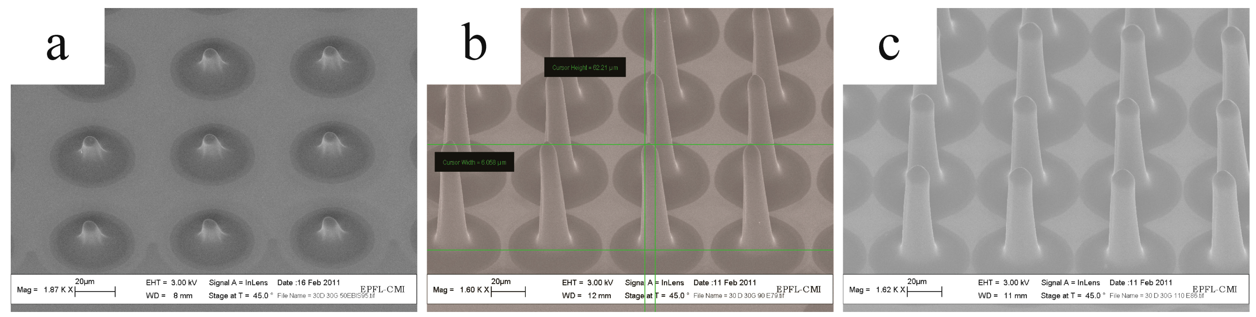
The alternative presented here is the use of a digital micromirror device (DMD) chip from Texas Instruments Inc. (Dallas, TX, USA) and relies on the same spatial and temporal light modulation technology used in DLP (digital light processing) projectors and other consumer electronics. A commercial instrument based on this chip is offered by Intelligent Micro Patterning LLC (St. Petersburg, FL, USA). An enormous simplification of lithography hardware is feasible by using the movable mirror arrays in a DMD chip to project images on the photoresist. No grayscale masks are needed. This technique is capable of fabricating micromachined elements with complex surface topographies and can be used for implementing maskless binary and grayscale lithography. Although the current resolution of this maskless photolithography (submicron) is far less than with e-beam lithography (~10 nm) or laser writers (<1.0 μm), it is a parallel technique, and for many applications, microfluidics for example, the lower resolution might not be an obstacle. Unfortunately, the maximum field of exposure is currently only a few millimeters square (decreasing inversely proportional to resolution) and image stitching, available in commercial systems, is necessary if a large-area pattern is to be fabricated. The unique capability of implementing a gray scale is probably the most essential merit of this maskless lithography system. When a mirror is switched on more frequently than off, it reflects a light gray pixel; a mirror that is switched off more frequently reflects a darker gray pixel. In this way, the mirrors in a DMD system can reflect pixels in up to 1024 shades of gray to convert the video or graphic signal entering the DMD chip into a highly-detailed grayscale image. Examples of SU-8 grayscale features obtained with this type of maskless lithography are shown in Figure 2. The characterization of the exposure dose depending on the grayscale used in software, as well as other processing parameters, have been detailed elsewhere by this author and his collaborators [42].
Figure 2.
Examples of SU-8 structures fabricated using an SF-100 Grayscale Lithography equipment from Intelligent Micro Patterning: (a) Bridges, (b) A cover for a pillar array, and (c) Suspended structures of different thickness.
Figure 2.
Examples of SU-8 structures fabricated using an SF-100 Grayscale Lithography equipment from Intelligent Micro Patterning: (a) Bridges, (b) A cover for a pillar array, and (c) Suspended structures of different thickness.

3. Carbonization
Carbonization is the process by which solid residues with a high content of carbon are obtained from organic materials, usually by pyrolyzing them in an inert atmosphere. Different precursors to glass-like carbon exist, including phenolic resins, polyfurfuryl alcohols, cellulose, polyvinyl chloride and polyimides [43,44,45,46,47,48,49,50,51,52,53]; and the degree of shrinkage and carbon yield, the ratio of the weight of carbon to the weight of the original polymer sample, varies depending on the choice. For example, phenol-formaldehyde, polyfurfuryl alcohol and polyvinyl alcohol have the highest yields, with approximately 50% carbon. The amount of cross-linkage in the polymer matrix has also been shown to play a role in shrinkage [54].
In this work, carbonization of SU-8 takes place in a furnace under a nitrogen atmosphere, established by flowing N2 at 2000 mL/min. Both quartz and alumina tubes with internal diameter ranging from 120 to 140 mm have been used. The protocol features three stages: (1) a temperature ramp from room temperature to 200 °C at 10 °C/min, followed by a 30-min dwell at 200 °C; this step is to completely eliminate the solvent and allow for any residual oxygen to be evacuated from the chamber and to prevent combustion of the polymer as the temperature is raised further [17]; (2) a temperature ramp from 200 to 900 °C at 10 °C/min with a one-hour dwell at 900 °C to complete carbonization; and (3) a natural cool down to room temperature by turning the furnace off. Carbonization is a complex process with many reactions taking place concurrently, including dehydrogenation, condensation, hydrogen transfer and isomerization [3,55,56,57,58,59,60]. The pyrolysis process of organic compounds can be divided into three major steps: (1) pre-carbonization, (2) carbonization and (3) annealing. During pre-carbonization (T < 300 °C), molecules of solvent and unreacted monomer are eliminated from the polymeric precursor. The next step, carbonization, can be further divided into two sub-stages: (i) from 300 to 500 °C, when heteroatoms, such as oxygen and halogens, are eliminated, causing a rapid loss of mass, while a network of conjugated carbon systems is formed and hydrogen atoms start being eliminated; and (ii) from 500 to 1200 °C, where hydrogen, oxygen and nitrogen atoms are completely eliminated and the aromatic network is forced to become interconnected. At this point, permeability decreases and density, hardness, the Young’s modulus and electrical conductivity increase. The final step, annealing, should be carried out at temperatures above 1200 °C to allow for the gradual elimination of any structural defects and the evolution of any further impurities. The final pyrolysis temperature determines the degree of carbonization and the residual content of foreign elements. Here, where the final temperature is 900 °C, the carbon content of the residue is expected to exceed a mass fraction of 90% in weight. At T ≈ 1300 °C more than 99% carbon can be found [61].
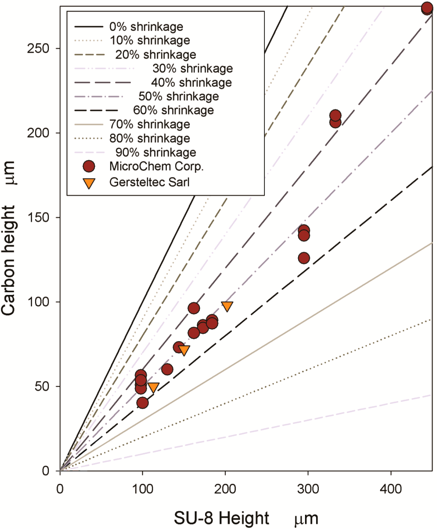
As expected, the SU-8 precursor structures shrink during carbonization. Here, I present the results obtained when carbonizing SU-8 structures with the same footprint, but different heights. Results are presented in Figure 3. The precursor microstructures were made using SU-8 2150 from MicroChem or GM1075 from Gersteltec Sárl, as indicated in the figure. Shrinkage percentage, calculated as one-carbon height/SU-8 height, varies from ~37% to 60% and seems to be inversely proportional to the height of the precursor SU-8; it appears to be independent from the choice of provider. Furthermore, the shrinkage obtained at all dimensions is slightly less than isometric [31], due to the fact that the structures are bound to a surface during pyrolysis and their shrinkage in the X-Y plane is somewhat restricted. The shrinkage of free-standing parts has been shown to be isometric [22]. Cross-linkage in the SU-8 matrix was not quantified, but processing guidelines from the manufacturers were followed in all cases. One plausible explanation of the shrinkage dependence on the height of the SU-8 precursor is the change of the surface-to-volume ratio as the height increases. The surface area of a pillar with diameter D and height h is given by πD2/4 + πDh, while its volume is given by πD2h/4. The surface area-to-volume ratio, SV, is thus 1/h + 4/D, and since D remains constant for all the pillars, SV is inversely proportional to h. Interestingly, this relation 1/h is qualitatively similar to the shrinkage-precursor height obtained experimentally. As noted before by other authors [62], thick layers may impede efficient degassing of the various products of the carbonization process. Ongoing work is characterizing both the mechanisms behind the dependence of shrinkage to precursor height and the carbonization process of SU-8 at temperatures above 900 °C, where a higher percentage of carbon is expected. Such an increased percentage may improve the mechanical and electrical properties of the glass-like carbon, yielding better components in a number of applications, including those presented next.
Figure 3.
The relation between the height of carbon structures and their SU-8 precursors when using SU-8 2150 from MicroChem (circles) and GM1075 from Gersteltec (downward triangles). Lines denote different degrees of shrinkage, from 0% to 90%. Note how shrinkage decreases as thicker structures are fabricated.

4. Selected Applications
Several applications have been demonstrated using carbon structures derived from SU-8 patterned with photolithography, including capacitors [63], batteries [64,65] and a number of electrochemical sensors. Here, I will provide a short overview on two applications: (1) bioparticle sorting using carbon-electrode DEP; and (2) micromolding of bulk metallic glasses (BMG) using carbon structures.
4.1. Carbon-Electrode Dielectrophoresis
Dielectrophoresis (DEP) is a field-based technique enabling the selective manipulation of a targeted particle, or population of particles, using the interaction of a non-uniform electric field with the induced effective dipole moment of the targeted particle(s). DEP is advantageous over other particle separation techniques, such as flow cytometry and MACS® (Magnetic-activated cell sorting), because discrimination between different particles is based solely on their intrinsic physical properties, such as surface structure and internal compartmentalization, and not on external tags, like antibody-linked fluorophores or magnetic nanoparticles; which tend to be expensive. The inherent physical properties of a particle will determine its dielectric properties and give it a characteristic dielectric phenotype. DEP has been demonstrated in a variety of applications, ranging from the manipulation of cells and bacteria, to the separation of proteins and other molecules.
One of the requirements to induce a DEP force on a sample is the creation of a non-uniform electric field to create volumes of different field magnitudes across the sample. A number of techniques have been developed to establish such a field gradient throughout a sample, and the reader is directed to the recent extensive review on such techniques by the current author [66]. The innovation presented here is the use of 3D glass-like carbon electrodes to induce a DEP force on targeted particles flowing inside a fluidic network. This technique, known as carbon-electrode dielectrophoresis, or carbon DEP, has been validated in a number of applications and provides several advantages over more traditional DEP techniques. Perhaps the most important is the fact that high aspect ratio structures can cover the entire height of a flow channel, greatly improving the throughput and efficiency of DEP devices by reducing the mean distance of any particle to the closest electrode surface. This way, one may increase the cross-sectional area of the channel, to increase the flow rate and throughput, and still be able to address each and every particle flowing through the channel, to improve efficiency. Additionally, glass-like carbon features a wider electrochemical stability window than platinum and gold, meaning a stronger electric field and DEP force can be applied to a sample without electrolyzing it.
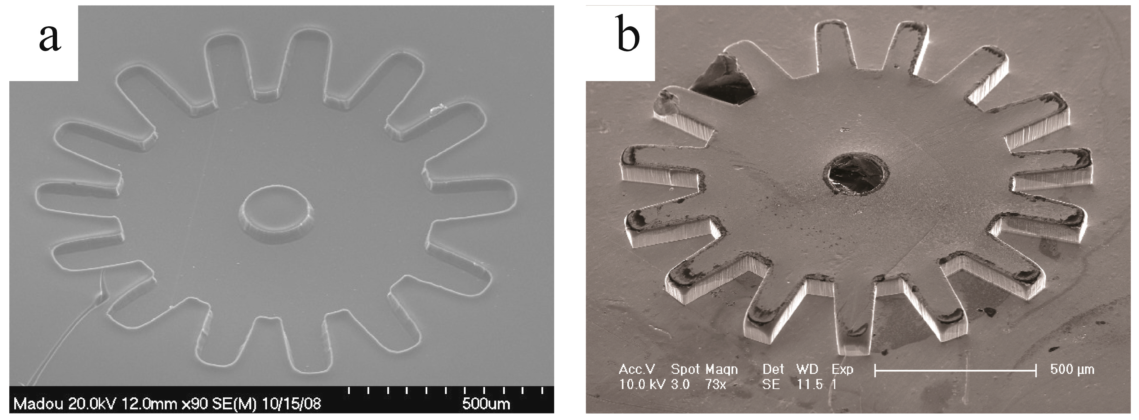
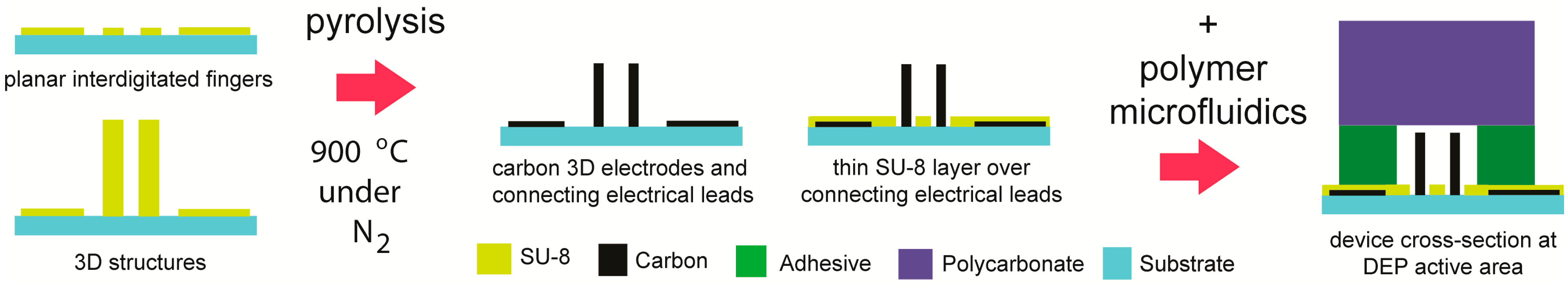
SU-8 photolithography is used to fabricate the high aspect ratio structures serving as carbon precursors, as detailed elsewhere [31]. The complete fabrication process is illustrated in Figure 4. The process starts with the photo-patterning of the carbon precursor on a rigid substrate, either silicon or fused silica, capable of withstanding the elevated temperatures needed for carbonization. SU-8 photolithography is implemented in two steps: (1) fabrication of planar interdigitated fingers that will become carbon connection leads to the base of the 3D carbon electrodes; and (2) fabrication of SU-8 pillars that will become the 3D carbon electrodes. The process parameters are optimized to fabricate structures featuring gaps in between them as narrow as 15 μm. Furthermore, the implementation of a hard bake at 190 °C after the development of the SU-8 structures is crucial to improve the adhesion of SU-8 to the substrate and to prevent the SU-8 from peeling off during pyrolysis. The SU-8 patterns are carbonized in a furnace under a nitrogen atmosphere, as detailed above. After pyrolysis, a thin layer, ~2 μm, of SU-8 is patterned around the carbon electrodes to electrically insulate the connection leads and to planarize the surface around the base of the electrodes. The microfluidic network is fabricated separately from the carbon electrodes and is made by stacking double-sided pressure-sensitive adhesive and polycarbonate or PMMA. The adhesive layer can be patterned using a cutting plotter, while holes in the polymer are made manually or by using a CNC-enabled mill (CNC stands for Computer Numerical Control). The microfluidics network is then manually positioned around the carbon electrode array, and the arrangement is sealed using a cold rolling press.
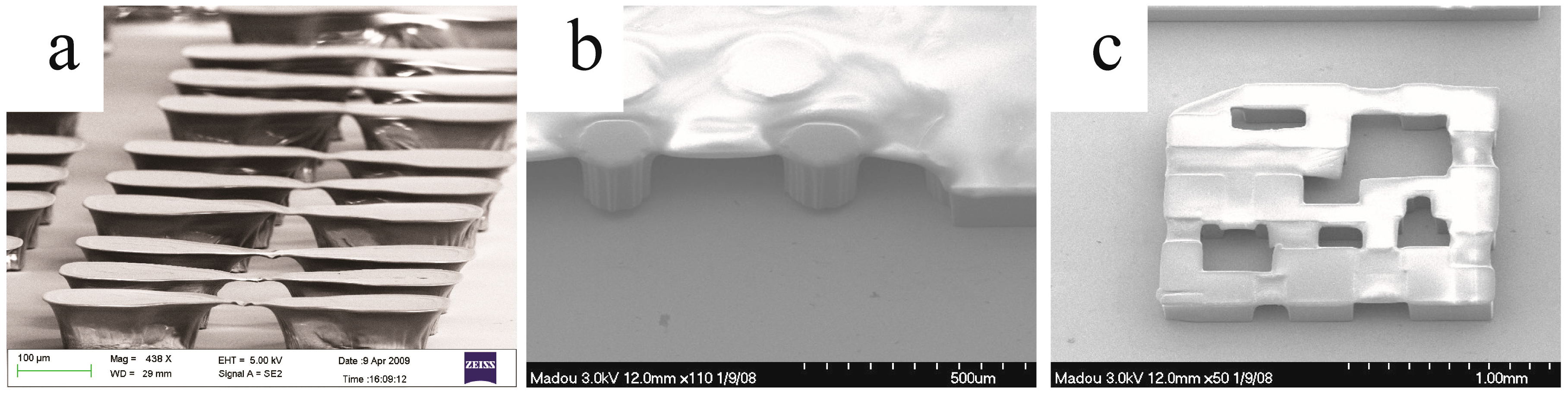
Figure 4.
Fabrication sequence of microfluidics devices featuring carbon electrodes. These devices are then used to implement active filters using dielectrophoresis (DEP).
Figure 4.
Fabrication sequence of microfluidics devices featuring carbon electrodes. These devices are then used to implement active filters using dielectrophoresis (DEP).
A number of applications have been demonstrated using these 3D carbon DEP devices. The motivation is to use them as active filters for the trapping and purification of selected cells, bacteria and molecules. The experimental protocol usually features three main stages: (1) extract targeted particles from the sample by trapping them on the electrode array using DEP; (2) holding the particles on the electrode array by DEP forces, while a washing solution is flowed through the channel; and (3) releasing the now-washed targeted particles, by de-polarizing the electrode array, for collection at the exit of the channel. In such way, one can enrich and purify a selected particle population from a given sample. A number of applications have been demonstrated [24,67], and the latest include: (i) elimination of natural contaminants to increase the sensitivity of polymerase chain reaction (PCR)-based protocols [68]; (ii) enrichment of bacterial persisters from an antibiotic-treated sample [69]; (iii) trapping of lambda DNA [70]; and (iv) cell lysis [71]. Current work on the integration of these stages in a sample preparation system towards a sample-to-answer platforms for diagnostics is being performed.
4.2. Carbon Micromolds
Rigid materials, such as metals or ceramics, are still preferred over lower cost polymers in the fabrication of micromolds, since the later tend to lose their integrity under certain temperature and pressure conditions. Silicon-based materials are often employed for experimental or small productions, as they offer a rigid mold, but the brittleness makes them hard to handle. If a lasting mold is the objective, metals, like Ni or carbide alloys (tungsten or silicon carbide), are among the materials of choice. Current techniques in mold fabrication include micro-CNC machining, electrical discharge machining (EDM), laser ablation, electrochemical machining (ECM), deep reactive ion etching (DRIE), focused ion beam milling and LIGA (a German acronym for Lithographie, Galvanoformung, Abformung), a combination of X-ray lithography and electroplating. Despite its lengthy process and initial high cost, the most widely accepted technique to fabricate micromolds is indeed LIGA, a German acronym for lithography, electroplating and molding. In this technique, X-ray lithography is used to derive a polymer mold and then used as a template for electroplating a desired metal, usually Ni. The main advantage of LIGA is its capability to achieve very high aspect ratio structures thanks to the use of X-ray lithography. Unfortunately, the need of a synchrotron hinders the adoption of LIGA by a larger number of commercial applications. Photolithography of SU-8 in combination with electroplating offers an affordable alternative to LIGA and is sometimes referred to as “poor man’s LIGA”.
Here, glass-like carbon micromolds are proposed as an alternative to those made using LIGA. The method developed makes use of traditional photolithography on a polymer film to derive free-standing SU-8 parts, as detailed in Section 2.1 (see Supplementary, Figure S2). Following the protocol detailed in Section 3 attains the carbonization of these structures. The resultant carbon molds comply with the mechanical and thermal integrity of a permanent mold, and yet, they are fabricated at a cost that enables their potential use as sacrificial molds. The mold fabrication process consists of two steps, photolithography and pyrolysis, and does not employ electroplating. Glass-like carbon has been shown to poses a nearly atomic-flat surface [14] and features a melting temperature above 3000 °C in inert atmospheres. The use of a releasable polymer film in photolithography further reduces processing costs and enables the carbonization of free-standing SU-8 parts [22]. This last part is extremely important to maintain the fidelity of the carbon shape with respect to the SU-8 precursor. If the carbon precursor is adhered to a surface of another material, silicon for example, the difference between their coefficients of thermal expansion leads to distortion of the carbon shape at the interface [22].
Glass-like carbon structures were validated as micromolds by shaping bulk metallic glasses (BMG) [22,72]; a class of metal alloys featuring high strength, a large elastic strain limit and a high corrosion resistance, due to their amorphous nature. BMGs are isotropic, homogeneous and free from any crystalline defects down to atomic scales [73,74]. Such properties make these materials excellent candidates for miniaturized scale applications, including MEMS, precision surgery tools and watch movement components. BMGs can be thermoplastically formed (TPF) like plastics [75], but the main limiting factor in the TPF of BMGs is in the type of master molds required to guarantee stability under TPF temperatures (200–450 °C) and pressures (10–30 MPa). Unfortunately, under such conditions, polymer molds used for electroplating are not an option. However, the carbonization of such polymer molds yields a low cost, robust, glass-like carbon mold. The details of the fabrication and use of carbon molds for BMG shaping are detailed elsewhere by this author and his collaborators [22]. Briefly, BMG molding was conducted using custom heating plates (top and bottom) installed on a load cell of an Instron mechanical testing machine. Carbon molds were placed on the bottom plate and heated to 430 °C, while a pellet of BMG was placed on top of the mold and pressed at 10 MPa for different time intervals. The results are shown in Figure 5 for the case of a BMG gear. Note that in this preliminary test, the BMG comes with a carbon residue after de-molding (Figure 5b). Oxygen plasma was used to remove such residues followed by a sonicated bath in acetone. Ongoing work on the characterization of achievable geometries and optimization of the side wall angle to facilitate de-molding, as well as characterization of repeatability and dimensional tolerance is being performed. The use of grayscale lithography to fabricate the carbon structures is also under investigation.
Figure 5.
Molding of a bulk metallic glass gear (b) using the glass-like carbon micromold shown in (a). Black portions in (b) are carbon residues from the de-molding operation.
Figure 5.
Molding of a bulk metallic glass gear (b) using the glass-like carbon micromold shown in (a). Black portions in (b) are carbon residues from the de-molding operation.

5. Conclusions
Besides versatility, photolithography offers high resolution and the use of standardized equipment and commercial photoresists. A variety of shapes in different dimensions can be made by optimizing one or more parameters, such as the type of exposure or the kind of substrate. The photopatterned SU-8 structures can then be carbonized by high temperature heat treatment in an inert atmosphere. Shrinkage during this process has been partially characterized and found to be highly reproducible when using SU-8 photoresists from current vendors. The resultant glass-like carbon is chemically very inert, electrochemically and mechanically stable, as well as electrical conductive. Indeed, these properties have made glass-like carbon the material of choice in a number of applications, from energy to healthcare diagnostics.
Supplementary Materials
Supplementary materials can be accessed at: https://www.mdpi.com/2072-666X/5/3/766/s1.
Acknowledgements
The author acknowledges collaboration in developing some of the results presented here: in grayscale lithography with Ashutosh Sharma and Prabhat Dwivedi at the Indian Institute of Technology, Kanpur; and in micromolding with Jan Schroers in Yale University and Golden Kumar at Texas Tech University.
Conflicts of Interest
The author declares no conflict of interest.
References
- Jenkins, G.; Kawamura, K. Structure of glassy carbon. Nature 1971, 231, 175–176. [Google Scholar] [CrossRef]
- Pesin, L.A. Structure and properties of glass-like carbon. J. Mater. Sci. 2002, 37, 1–28. [Google Scholar] [CrossRef]
- Jenkins, G.; Kawamura, K.; Ban, L. Formation and structure of polymeric carbons. Proc. R. Soc. Lond. A Math. Phys. Sci. 1972, 327, 501–517. [Google Scholar] [CrossRef]
- Kakinoki, J. A model for the structure of “glassy carbon”. Acta Crystallogr. 1965, 18, 578. [Google Scholar] [CrossRef]
- Fitzer, E.; Kochling, K.H.; Boehm, H.P.; Marsh, H. Recommended terminology for the desciption of carbon as a solid. Pure Appl. Chem. 1995, 67, 473–506. [Google Scholar] [CrossRef]
- Zittel, H.E.; Miller, F.J.A. Glassy-carbon electrode for voltammetry. Anal. Chem. 1965, 37, 200–203. [Google Scholar] [CrossRef]
- Van der Linde, W.E.; Dieker, J.W. Glassy carbon as electrode material in electro-analytical chemistry. Anal. Chim. Acta 1980, 119, 1–24. [Google Scholar]
- Yamada, S.; Sato, H. Some physical properties of glassy carbon. Nature 1962, 193, 261–262. [Google Scholar] [CrossRef]
- Rothwell, W. Small-angle X-ray scattering from glassy carbon. J. Appl. Phys. 1968, 39, 1840–1845. [Google Scholar] [CrossRef]
- McFeely, S.P.; Kowalczyk, S.P.; Ley, L.; Cavell, R.G.; Pollak, R.A.; Shirley, D.A. X-ray photoemission studies of diamond, graphite, and glassy carbon valence bands. Phys. Rev. B 1974, 9, 5268–5278. [Google Scholar] [CrossRef]
- Pesin, L.A.; Baitinger, E.M. A new structural model of glass-like carbon. Carbon 2002, 40, 295–306. [Google Scholar] [CrossRef]
- Yoshida, A.; Kaburagi, Y.; Hishiyama, Y. Microtexture and magnetoresistance of glass-like carbons. Carbon 1991, 29, 1107–1111. [Google Scholar] [CrossRef]
- Spain, I. Electronic Transport properties of graphite, carbons, and related materials. In Chemistry and Physics of Carbon; Walker, P.L., Ed.; Marcel Dekker, Inc.: New York, NY, USA, 1981; pp. 119–304. [Google Scholar]
- Ranganathan, S.; McCreery, R.; Majji, S.M.; Madou, M. Photoresist-derived carbon for microelectromechanical systems and electrochemical applications. J. Electrochem. Soc. 2000, 147, 277–282. [Google Scholar] [CrossRef]
- Gelorme, J.; Cox, R.; Gutierrez, S. Photoresist Composition and Printed Circuit Boards and Packages Made Therewith. U.S. Patent 4,882,245, 21 November 1989. [Google Scholar]
- Singh, A.; Jayaram, J.; Madou, M.; Akbar, S. Pyrolysis of negative photoresists to fabricate carbon structures for microelectromechanical systems and electrochemical applications. J. Electrochem. Soc. 2002, 149, E78–E83. [Google Scholar] [CrossRef]
- Wang, C.; Jia, G.; Taherabadi, L.H.; Madou, M.J. A novel method for the fabrication of high-aspect ratio C-MEMS structures. J. Microelectromech. Syst. 2005, 14, 348–358. [Google Scholar] [CrossRef]
- Wang, C.; Madou, M. From MEMS to NEMS with carbon. Biosens. Bioelectron. 2005, 20, 2181–2187. [Google Scholar] [CrossRef] [PubMed]
- Amato, L.; Keller, S.S.; Heiskanen, A.; Dimaki, M.; Emnéus, J.; Boisen, A.; Tenje, M. Fabrication of high-aspect ratio SU-8 micropillar arrays. Microelectron. Eng. 2012, 98, 483–487. [Google Scholar] [CrossRef]
- Heo, J.I.; Shim, D.S.; Teixidor, G.T.; Oh, S.; Madou, M.J.; Shin, H. Carbon interdigitated array nanoelectrodes for electrochemical applications. J. Electrochem. Soc. 2011, 158, J76–J80. [Google Scholar] [CrossRef]
- Martinez-Duarte, R. Fabrication of Carbon Micro Molds; University of California: Irvine, CA, USA, 2009. [Google Scholar]
- Martinez-Duarte, R.; Madou, M.J.; Kumar, G.; Schroers, J. A novel method for amorphous metal micromolding using carbon MEMS. In Proceedings of Solid-State Sensors, Actuators and Microsystems Conference, Denver, CO, USA, 21–25 June 2009; pp. 188–191.
- Malladi, K.; Wang, C.; Madou, M. Fabrication of suspended carbon microstructures by E-beam writer and pyrolysis. Carbon 2006, 44, 2602–2607. [Google Scholar] [CrossRef]
- Martinez-Duarte, R.; Gorkin, R.A.; Abi-Samra, K.; Madou, M.J. The integration of 3D carbon-electrode dielectrophoresis on a CD-like centrifugal microfluidic platform. Lab Chip 2010, 10, 1030–1043. [Google Scholar] [CrossRef] [PubMed]
- Abgrall, P.; Conedera, V.; Camon, H.; Gue, A.M.; Nguyen, N.T. SU-8 as a structural material for labs-on-chips and microelectromechanical systems. Electrophoresis 2007, 28, 4539–4551. [Google Scholar] [CrossRef] [PubMed]
- Campo, A.; del Greiner, C. SU-8: A photoresist for high-aspect-ratio and 3D submicron lithography. J. Micromech. Microeng. 2007, 17, R81–R95. [Google Scholar] [CrossRef]
- Martinez-Duarte, R.; Madou, M. SU-8 photolithography and its impact on microfluidics. In Microfluidics and Nanofluidics Handbook: Fabrication, Implementation and Applications; Mitra, S., Chakraborty, S., Eds.; CRC Press: Boca Raton, FL, USA, 2009; pp. 231–268. [Google Scholar]
- Abgrall, P.; Lattes, C.; Conédéra, V.; Dollat, X.; Colin, S.; Gué, A.M. A novel fabrication method of flexible and monolithic 3D microfluidic structures using lamination of SU-8 films. J. Micromech. Microeng. 2005, 16, 113–121. [Google Scholar] [CrossRef]
- Yang, R.; Wang, W. A numerical and experimental study on gap compensation and wavelength selection in UV-lithography of ultra-high aspect ratio SU-8 microstructures. Sens. Actuators B Chem. 2005, 110, 279–288. [Google Scholar] [CrossRef]
- Chuang, Y.J.; Tseng, F.G.; Lin, W.K. Reduction of diffraction effect of UV exposure on SU-8 negative thick photoresist by air gap elimination. Microsyst. Technol. 2002, 8, 308–313. [Google Scholar] [CrossRef]
- Martinez-Duarte, R.; Renaud, P.; Madou, M. A novel approach to dielectrophoresis using carbon electrodes. Electrophoresis 2011, 32, 2385–2392. [Google Scholar] [PubMed]
- Martinez-Duarte, R. Label-Free Cell Sorting Using Carbon-Electrode Dielectrophoresis and Centrifugal Microfluidics; University of California: Irvine, CA, USA, 2010. [Google Scholar]
- Zhang, J.; Chan-Park, M.B.; Conner, S.R. Effect of exposure dose on the replication fidelity and profile of very high aspect ratio microchannels in SU-8. Lab Chip 2004, 4, 646–653. [Google Scholar] [CrossRef]
- Windt, D. L.; Cirelli, R.A. Amorphous carbon films for use as both variable-transmission apertures and attenuated phase shift masks for deep ultraviolet lithography. J. Vac. Sci. Technol. B. 1999, 17, 930–932. [Google Scholar] [CrossRef]
- Sure, A.; Dillon, T.; Murakowski, J.; Lin, C.; Pustai, D.; Prather, D. Fabrication and characterization of three-dimensional silicon tapers. Opt. Express 2003, 11, 3555–3561. [Google Scholar] [CrossRef] [PubMed]
- Taff, J.; Kashte, Y. Fabricating multilevel SU-8 structures in a single photolithographic step using colored masking patterns. J. Vac. Sci. Technol. A 2006, 24, 742–746. [Google Scholar] [CrossRef]
- Hirai, Y.; Inamoto, Y.; Sugano, K.; Tsuchiya, T.; Tabata, O. Moving mask UV lithography for three-dimensional structuring. J. Micromech. Microeng. 2007, 17, 199–206. [Google Scholar] [CrossRef]
- Yoon, Y.K.; Park, J.H.; Allen, M.G. Multidirectional UV lithography for complex 3-D MEMS structures. J. Microelectromech. Syst. 2006, 15, 1121–1130. [Google Scholar] [CrossRef]
- Ullal, C.K.; Maldovan, M.; Thomas, E.L.; Chen, G.; Han, Y.J.; Yang, S. Photonic crystals through holographic lithography: Simple cubic, diamond-like, and gyroid-like structures. Appl. Phys. Lett. 2004, 84. [Google Scholar] [CrossRef]
- Deubel, M.; von Freymann, G.; Wegener, M.; Pereira, S.; Busch, K.; Soukoulis, C.M. Direct laser writing of three-dimensional photonic-crystal templates for telecommunications. Nat. Mater. 2004, 3, 444–447. [Google Scholar] [CrossRef] [PubMed]
- Bertsch, A.; Lorenz, H.; Renaud, P. 3D microfabrication by combining microstereolithography and thick resist UV lithography. Sens. Actuators A Phys. 1999, 73, 14–23. [Google Scholar] [CrossRef]
- Rammohan, A.; Dwivedi, P.K.; Martinez-Duarte, R.; Katepalli, H.; Madou, M.J.; Sharma, A. One-step maskless grayscale lithography for the fabrication of 3-dimensional structures in SU-8. Sens. Actuators B Chem. 2011, 153, 125–134. [Google Scholar] [CrossRef]
- Nishikawa, K.; Fukuyama, K.; Nishizawa, T. Structure change of glass-like carbon with heat treatment, studied by small angle X-ray scattering: I. Glass-like carbon prepared from phenolic resin. Jpn. J. Appl. Phys. 1998, 37, 6486–6491. [Google Scholar]
- Jenkins, G.M.; Kawamura, K. Polymeric Carbon—Carbon Fibre, Glass and Char; Cambridge University Press: London, UK, 1976. [Google Scholar]
- Fitzer, E.; Schaefer, W.; Yamada, S. The Formation of glasslike carbon by pyrolysis of polyfurfuryl alcohol and phenolic resin. Carbon 1969, 7, 643–648. [Google Scholar] [CrossRef]
- Vohler, O.; Reiser, P.; Martina, R.; Overhoff, D. New forms of carbon. Angew Chem. Int. Ed. 1970, 9, 414–425. [Google Scholar] [CrossRef]
- Kawamura, K.; Kimura, S. Glass-like carbon made from epoxy resin cured with 2,4,6-trinitrophenol. Bull. Chem. Soc. Jpn. 1983, 56, 2499–2503. [Google Scholar] [CrossRef]
- Bhatia, G.; Aggarwal, R.; Malik, M.; Bahl, O. Conversion of phenol formaldehyde resin to glass-like carbon. J. Mater. Sci. 1984, 19, 1022–1028. [Google Scholar] [CrossRef]
- Neenan, T.; Callstrom, M.; Bachman, B.; McCreery, R.L.; Alsmeyer, D.C. Doped glassy carbon materials (DGC): Their synthesis from polymeric precursors and investigation of their properties. Br. Polym. J. 1990, 23, 171–177. [Google Scholar] [CrossRef]
- Schueller, O.J.A.; Brittain, S.T.; Whitesides, G.M. Fabrication of glassy carbon microstructures by pyrolysis of microfabricated polymeric precursors. Adv. Mater. 1997, 9, 477–480. [Google Scholar] [CrossRef]
- Shah, H.V.; Brittain, S.T.; Huang, Q.; Hwu, S.J.; Whitesides, G.; Smith, D.W. Bis-o-diynylarene (BODA) derived polynaphtalenes as precursors to glassy carbon microstructures. Chem. Mater. 1999, 11, 9078–9079. [Google Scholar]
- Hishiyama, Y.; Igarashi, K.; Kanaoka, I.; Fujii, H. Graphitization behavior of kapton-derived carbon film related to structure, microtexture and transport properties. Carbon 1997, 35, 657–668. [Google Scholar] [CrossRef]
- Gac, N.A.; Spokes, G.N.; Benson, S.W. Thermal degradation of nadic methyl anhydride-cured epoxy novolac. J. Polym. Sci. A 1970, 8, 593–608. [Google Scholar] [CrossRef]
- Fitzer, E.; Schäfer, W. The effect of crosslinking on the formation of glasslike carbons from thermosetting resins. Carbon 1970, 8, 353–364. [Google Scholar] [CrossRef]
- Lee, L.H. Mechanisms of thermal degradation of phenolic condensation polymers. II. Thermal stability and degradation schemes of epoxy resins. J. Polym. Sci. Part A 1965, 3, 859–882. [Google Scholar]
- Lyons, A.; Wilkins, C.; Robbins, M. Thin pinhole-free carbon films. Thin Solid Films 1983, 103, 333–341. [Google Scholar] [CrossRef]
- Nakagawa, H.; Tsuge, S. Studies on thermal degradation of epoxy resins by high-resolution pyrolysis-gas chromatography. J. Anal. Appl. Pyrolysis 1987, 12, 97–113. [Google Scholar] [CrossRef]
- Chen, K.S.; Yeh, R.Z. Pyrolysis kinetics of epoxy resin in a nitrogen stmosphere. J. Hazard. Mater. 1996, 49, 105–113. [Google Scholar] [CrossRef]
- Beyler, C.; Hirschler, M. Thermal decomposition of polymers. In SFPE Handbook of Fire Protection Engineering; National Fire Protection Association: Quincy, MA, USA, 2002; pp. 110–131. [Google Scholar]
- Ma, C.C.M.; Chen, C.Y.; Kuan, H.C.; Chang, W.C. Processability, thermal, mechanical, and morphological properties of novolac type-epoxy resin-based carbon-carbon composite. J. Compos. Mater. 2004, 38, 311–322. [Google Scholar] [CrossRef]
- Mehrotra, B.; Bragg, R.; Rao, A. Effect of heat treatment temperature (HTT) on density, weight and volume of glass-like carbon (GC). J. Mater. Sci. 1983, 18, 2671–2678. [Google Scholar] [CrossRef]
- Park, B.; Taherabadi, L.; Wang, C.; Zoval, J.; Madou, M.J. Electrical properties and shrinkage of carbonized photoresist films and the implications for carbon microelectromechanical systems devices in conductive media. J. Electrochem. Soc. 2005, 152, J136–J143. [Google Scholar] [CrossRef]
- Beidaghi, M.; Chen, W.; Wang, C. Electrochemically activated carbon micro-electrode arrays for electrochemical micro-capacitors. J. Power Sources 2011, 196, 2403–2409. [Google Scholar] [CrossRef]
- Min, H.S.; Park, B.Y.; Taherabadi, L.; Wang, C.; Yeh, Y.; Zaouk, R.; Madou, M.J.; Dunn, B. Fabrication and properties of a carbon/polypyrrole three-dimensional microbattery. J. Power Sources 2008, 178, 795–800. [Google Scholar] [CrossRef]
- Teixidor, G.T.; Zaouk, R.B.; Park, B.Y.; Madou, M.J. Fabrication and characterization of three-dimensional carbon electrodes for lithium-ion batteries. J. Power Sources 2008, 183, 730–740. [Google Scholar] [CrossRef]
- Martinez-Duarte, R. Microfabrication technologies in dielectrophoresis applications—A review. Electrophoresis 2012, 33, 3110–3132. [Google Scholar] [CrossRef] [PubMed]
- Jaramillo, M.D.C.; Torrents, E.; Martinez-Duarte, R.; Madou, M.J.; Juarez, A. On-line separation of bacterial cells by carbon-electrode dielectrophoresis. Electrophoresis 2010, 31, 2921–2928. [Google Scholar] [CrossRef] [PubMed]
- Jaramillo, M.D.C.; Martínez-Duarte, R.; Hüttener, M.; Renaud, P.; Torrents, E.; Juárez, A. Increasing PCR densitivity by removal of polymerase inhibitors in environmental samples by using dielectrophoresis. Biosens. Bioelectron. 2013, 43, 297–303. [Google Scholar] [CrossRef] [PubMed]
- Elitas, M.; Martinez-Duarte, R.; Dhar, N.; McKinney, J.D.; Renaud, P. Dielectrophoresis-based purification of antibiotic-treated bacterial subpopulations. Lab Chip 2014, 14, 1850–1857. [Google Scholar] [CrossRef] [PubMed]
- Martinez-Duarte, R.; Camacho-Alanis, F.; Renaud, P.; Ros, A. Dielectrophoresis of lambda-DNA using 3D carbon electrodes. Electrophoresis 2013, 34, 1113–1122. [Google Scholar] [CrossRef] [PubMed]
- Mernier, G.; Martinez-Duarte, R.; Lehal, R.; Radtke, F.; Renaud, P. Very high throughput electrical cell lysis and extraction of intracellular compounds using 3D carbon electrodes in lab-on-a-chip devices. Micromachines 2012, 3, 574–581. [Google Scholar] [CrossRef]
- Schroers, J.; Kumar, G.; Madou, M.; Martinez-Duarte, R. Carbon Molds for Use in the Fabrication of Bulk Metallic Glass Parts and Molds. U.S. Patent 2,012,0125,071 A1, 24 May 2012. [Google Scholar]
- Telford, M. The case for bulk metallic glass. Mater. Today 2004, 7, 36–43. [Google Scholar] [CrossRef]
- Johnson, W.L. Bulk amorphous metal—An emerging engineering material. JOM 2002, 54, 40–43. [Google Scholar] [CrossRef]
- Schroers, J.; Pham, Q.; Desai, A. Thermoplastic forming of bulk metallic glass—A technology for MEMS and microstructure fabrication. Microelectromech. Syst. J. 2007, 16, 240–247. [Google Scholar] [CrossRef]
© 2014 by the author; licensee MDPI, Basel, Switzerland. This article is an open access article distributed under the terms and conditions of the Creative Commons Attribution license (http://creativecommons.org/licenses/by/3.0/).
Share and Cite
MDPI and ACS Style
Martinez-Duarte, R. SU-8 Photolithography as a Toolbox for Carbon MEMS. Micromachines 2014, 5, 766-782. https://doi.org/10.3390/mi5030766
AMA Style
Martinez-Duarte R. SU-8 Photolithography as a Toolbox for Carbon MEMS. Micromachines. 2014; 5(3):766-782. https://doi.org/10.3390/mi5030766
Chicago/Turabian StyleMartinez-Duarte, Rodrigo. 2014. "SU-8 Photolithography as a Toolbox for Carbon MEMS" Micromachines 5, no. 3: 766-782. https://doi.org/10.3390/mi5030766