1. Introduction
As semiconductor technology scaling becomes increasingly difficult, 3D stacking has recently gained attention due to its potential to offer much higher form factor along with higher performance and lower power compared to 2D designs. 3D stacking can be achieved in many different ways: package-to-package stack, die-to-die stack, die-to-wafer stack, and wafer-to-wafer stack. Package-to-package stack and die-to-die stack allow selection of known good dies for stacking and, thus, provide higher yield but limited performance improvement compared to 2D. In addition, these have higher cost as each die needs to be handled individually while building a stacked module [
1,
2,
3]. The through-silicon-via (TSVs) used in package and die level stacks are typically larger in size thereby limiting the bandwidth and performance offered by these. On the other end, wafer-to-wafer 3D stack allows TSVs to be scaled by 20 times thereby allowing much higher bandwidth and performance improvement along with lowest manufacturing cost by allowing stacking of wafers instead of chip and thereby supporting volume production. However wafer-stacking technology can potentially suffer from compounded yield loss, but this can be mitigated by the use of innovative circuit design, fault tolerant and repair techniques. Due to the strong consumer demand for higher performance in a smaller size with lower cost 3D technology, the industry is moving towards wafer level stacked technology.
The scaling of TSVs depends on the aspect ratio (DTSV/TSi) of TSV diameter (DTSV) to thickness of silicon (TSi), which in turn is governed by techniques used to etch, deposit the oxide and plating of TSVs. Thus silicon thickness must scale with TSV diameter for fixed aspect ratio. Handling of thin die is more difficult than handling of thin wafers and thus wafer stacking supports smaller TSVs and TSV keep out, and much higher 3D connection density thereby allowing much higher bandwidths. Also, by allowing TSVs to directly land on a wiring level, the need of micro-pillars for 3D communication is eliminated in wafer stacking, thereby overcoming the limitation imposed by limited scaling of micro-pillar pitch, and, thus, favoring further scaling of TSV pitch that supports higher bandwidth.
Two key applications for wafer stacking are envisioned to be (a) massively parallel simple cores; (b) scaling of commodity memory. The increasing cost of lithography, and reliability and yield issues associated with the scaling of technology have made the cost reduction with scaling of technology node very difficult. Wafer scale 3D stacking allows scaling with existing technology nodes. Prior work [
3] has presented wafer-scale integration with tungsten TSV for low-power applications.
In this paper we present the stacking of high performance POWER7™ cache cores [
4] in 45 nm SOI technology with EDRAM and 13 metal levels. Five micrometer diameter electrically isolated Cu TSVs at 13 µm pitch are used for power delivery and signal communication in the stacked cache cores. Wafers are aligned and joined using low temperature oxide bonding after nine levels of metals. The wafers are thinned to 13 µm using grind polish and etch. TSVs are defined post bonding and thinning using conventional alignment techniques. Up to four additional metal levels are formed post bonding and TSV definition.
The remainder of this paper is organized as follows:
Section 2 provides a review of the existing methods for wafer-scale bonding along with a comparison of how the existing methods differ from our method of oxide bonding. The details of our wafer stacking 3D technology and process flow are described in
Section 3.
Section 4 describes the hardware test results and analysis. Finally, conclusions are presented in
Section 5.
2. Previous Work
Wafer-scale bonding can yield important benefits with respect to 3D integration. Among these are micro-scale interconnects (IC) with lower IC delay, very high data bandwidth due to the tighter possible IC pitch, and lower power consumption. In addition, very high throughput is achievable as multiple chips are bonded in parallel fashion and singulated later. As a result, cost savings and high-volume manufacturing can be achieved. With minimal modifications and additions to current manufacturing infrastructure, wafer-scale integration is possible, provided a suitable bonding approach is selected. There are several options regarding the wafer bonding approach, several of which are discussed below.
2.2. Hybrid Bonding
In this wafer bonding process, bonding of the metallic features on the surface of the wafers (for direct electrical connectivity) are accompanied by the bonding of the surrounding dielectric surfaces, either oxide or polymer, depending on the exact method used [
9]. The dielectric can be oxide inter layer dielectric (ILD) or polymer (
i.e., BCB). Special surface preparation steps are used, such as chemical mechanical polishing, plasma and/or wet cleans for surface cleaning and surface termination/activation. Typically, low surface topography and atomically smooth roughness is required, although use of recessed metal structures with respect to the dielectric is common. The bonding typically involves an initial room temperature bonding step to preserve alignment, followed by a thermal compression bonding step in the case of polymer/metal hybrid bonding, which ensures bonding of both metal-metal and polymer-polymer surfaces and establishes electrical connectivity.
This approach features the advantage of direct electrical connection and the high bond strength typical in metal-metal bonding interfaces, It does not require under fill, which is an advantage
vs. metal-metal bonding schemes, in order to address mechanical stability. However, the bonding overlay/alignment performance on a wafer-scale must be very accurate, especially for smaller CD features, and the scaling of interconnections CD and pitch can be more challenging
vs. oxide bonding and may limit the application when dense interconnecting schemes are needed [
10,
11]. There is also the question of reliability, as Cu surfaces are not enclosed in impenetrable barriers and are open/bonded to the ILD dielectric (oxide or polymer). Thermal and mechanical stress can be a concern for process yield in the case of polymer/metal hybrid bonding. Overall, throughput can be a concern, especially if thermal compression steps are involved.
2.3. SiO2 Bonding
This wafer bonding process generally involves the formation and preparation of silicon oxide bonding layers on the host and donor wafers and then activation and cleaning of the bonding layers with plasma and aqueous cleaning treatment, followed by loading the wafers, aligning, initiating contact, releasing the wafers to spread the bonding, and finally a post-bonding anneal to promote full-strength covalent bonding between the wafers [
12].
Oxide-to-oxide bonding is a highly promising front-up choice due to several significant advantages with regard to manufacturability, flexibility, and reliability. It features stable, insulating bonding layers and interfaces and a high-throughput process when compared to thermal compression bonding. The use of oxide layers provides flexibility with respect to overcoming topography. Bonding alignment performance can be accurate and stable, as initial bonding (which locks the alignment) is at room temperature. In addition to throughput advantages, this technique avoids increased thermal and mechanical stresses that are inherent in thermal compression bonding. Furthermore, as it does not involve direct electrical connections at bonding, it does not present as big a challenge with respect to reliability as metal-metal or hybrid bonding, where misalignment during bonding and/or insufficient under fill process performance can lead to issues, such as copper poisoning, migration/diffusion, mechanical robustness, etc. Lastly, oxide bonding is most amenable to further IC scaling of CD and pitch via TSV scaling, which can be much smaller than the typical micro-bump based schemes.
3. Wafer Level 3D Integration Process
High-speed Power7™ L3 processor cache prototype [
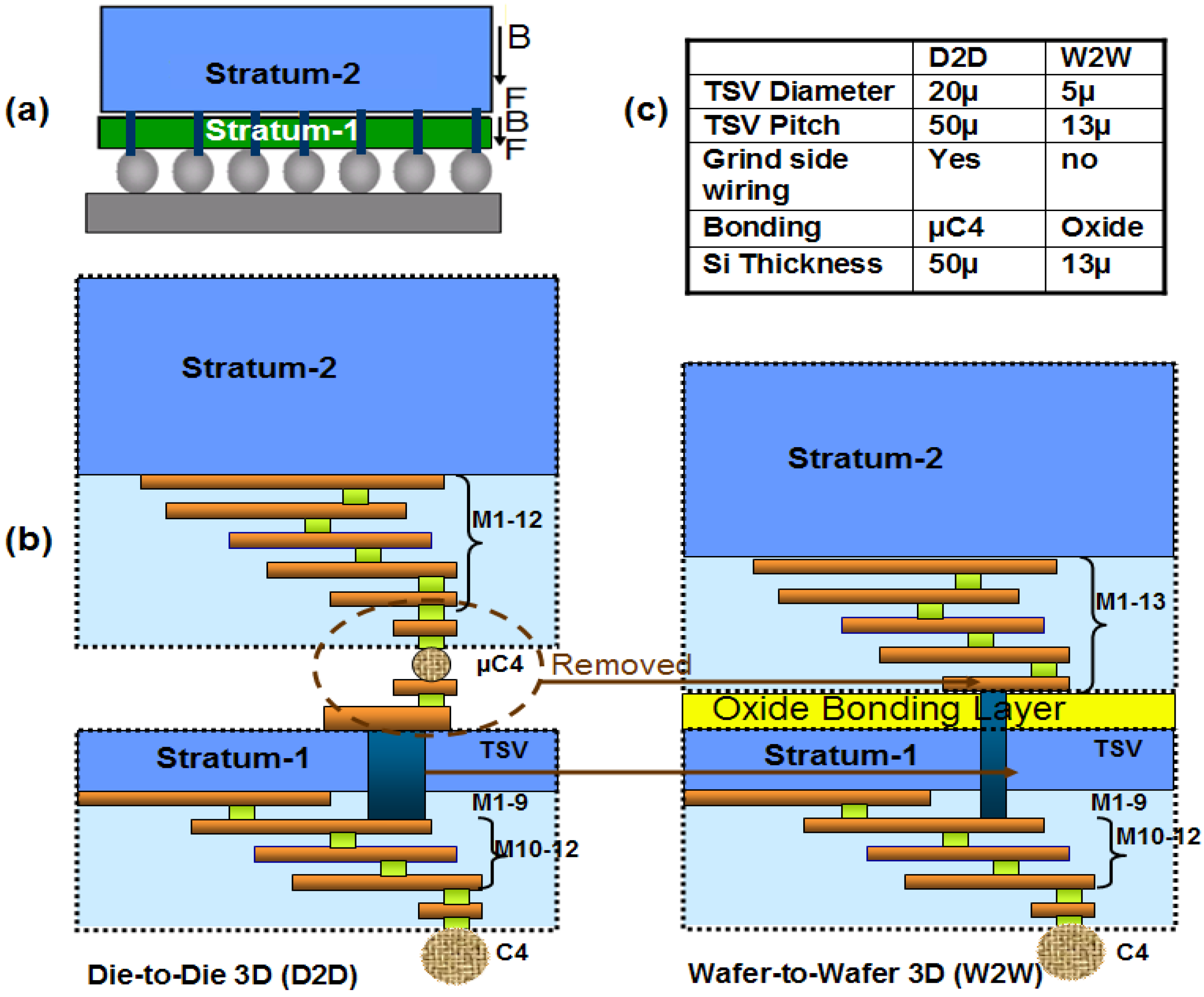
13], TSV chains, and FET structures originally designed for 3D die stacking were modified for wafer scale bonding. Backside wiring in the die stacking process was mapped to the front side top most level of the thick wafer (Stratum-2) (
Figure 1a,b) to provide a landing pad for the 5 μm copper TSVs. The comparison of die stacking and wafer 3D stacking technologies is shown in
Figure 1c. In addition to offering smaller TSV and TSV pitch, wafer stacking using oxide bonding compared to micro-bump-based bonding in die stacking. Additionally, die stacking requires additional grind side wiring levels for connection with TSV and pad formation for micro-bump which are no longer required in wafer stacking [
14].
Three-hundred-millimeter silicon wafers with 45 nm CMOS devices and 13 wiring levels were stacked similar to Obha
et al. [
15] with three differences. First, the wafers were joined using a low temperature (<400 °C) oxide bonding process instead of polymer adhesive. Second, the thick glass handle wafer used to support the device wafer during thinning was replaced by a thick blank silicon handle wafer. Third, the silicon handle wafer was attached using an oxide bonding step instead of temporary adhesive [
12]. After thinning the device wafer (Stratum-1) to 10–12 µm, the handle wafer was removed from the stack using a combination of mechanical grinding, reactive ion etch (RIE), and wet chemical thinning. These steps employ conventional silicon fabrication equipment and processes.
Figure 1.
(a) Schematic representation of wafer level 3D stacking; (b,c) Comparison of die-to-die (D2D) and wafer-to-wafer (W2W) 3D stacking technologies.
Figure 1.
(a) Schematic representation of wafer level 3D stacking; (b,c) Comparison of die-to-die (D2D) and wafer-to-wafer (W2W) 3D stacking technologies.
The oxide bonding process used in this work utilizes a dual oxide bonding layer deposited by use of chemical vapor deposition processes. The first film was optimized so as to overcome incoming wafer topography, as bonding surface flatness and absence of short/medium range topography is crucial for defect-free bonding. The film underwent a special annealing step that improves overall cleanliness and density of the surface and enhances the adhesion properties with respect to the second layer. A special polishing step was used to achieve sufficient bonding surface flatness, followed by a special cleaning step. Subsequently, the second bonding layer was deposited, which serves as the primary bonding layer. Special thermal annealing to improve its density and overall cleanliness was used, and a polishing step to ensure suitable roughness that is amenable to oxide bonding [
12]. Oxide bonding surfaces characterized using atomic force microscopy (AFM) after the bond film preparation is concluded, are typically shown to be atomically smooth with root mean square (RMS) roughness values between 0.2 nm and 0.4 nm. Thus, a smooth bonding surface is achieved, which is required for the bonding process.
Both host and donor wafers receive the same bonding layer preparation and surface cleaning and then are loaded to the oxide bonding platform where they undergo dual frequency nitrogen plasma activation, followed by de-ionized water megasonics clean. This step is needed to ensure removal of large particles that could result in bonding voids and also terminates the activated hydrophilic surface with silicon to hydroxyl bonds. Once both wafers are activated and cleaned, they are loaded to bonding chucks and they are aligned for bonding. The alignment positions are based on detection of alignment keys patterned on the wafers during the last metal level fabrication. Once the alignment is completed, the wafers are brought in close proximity a few microns from each other. At that point a small piston applies a force on the backside of the top wafer enough to bend it to initiate contact with the bottom wafer. Strong van der Waals bonds between the activated oxide surfaces are formed at the area of contact. After a brief waiting period to lock in the initial bond alignment the top wafer is allowed to relax on the surface of the bottom wafer and a bonding wave from the initially bonded area at the center propagates to the edge of the wafers. Then, the bonded wafer pairs are transferred without bonding overlay alignment deterioration to an anneal furnace, where the anneal can promote strong full-covalent bonding.
For the purposes of this work, a blank silicon wafer was bonded to the device wafer for use as handler. The silicon handler wafer was attached using the low-temperature oxide bonding method. The device wafer was then thinned from the backside to a thickness of 10–13 µm by using a combination of mechanical grinding, reactive ion etch (RIE), and wet chemical thinning, all these processes employing conventional silicon fabrication equipment and processes. An oxide layer was then prepared on the backside of the device wafer and then the stack was bonded to another paired full-thickness device wafer, with the blanket handler wafer now at the top of the stack. The handler wafer was then removed from the stack, also by a combination of mechanical grinding, reactive ion etch (RIE), and wet chemical thinning.
After stacking and removal of the handler, 5 µm diameter copper TSV interconnects were formed by use of deep RIE etching from the front side of stratum-1 (
Figure 2 and
Figure 3) using a process designed to handle the complex interlayer dielectric stacks, bond interface, and thinned silicon. The TSVs were lined with conformal oxide insulator liner by sub-atmospheric chemical vapor deposition (SACVD). Another RIE step was used to open the TSV insulator at the bottom of the TSVs. This was followed by TSV metallization, which involves metal liner and Cu seed deposition with physical vapor deposition (PVD) methods and finally bottom-up copper plating to fill the TSVs. In this fashion, TSVs with critical dimensions (CD) at 5 µm at a 13 µm pitch were fabricated.
Three additional copper wiring levels were then fabricated on stratum-1. Low resistivity copper TSVs integrated with copper wiring is essential to limit IR voltage drop for high-performance and low-voltage applications [
2,
16]. All processing and tools are compatible with advanced metal gate down to at least the 14 nm technology node and the TSV diameter is scalable to 1 µm. The face-to-back process can be repeated to stack multiple wafers.
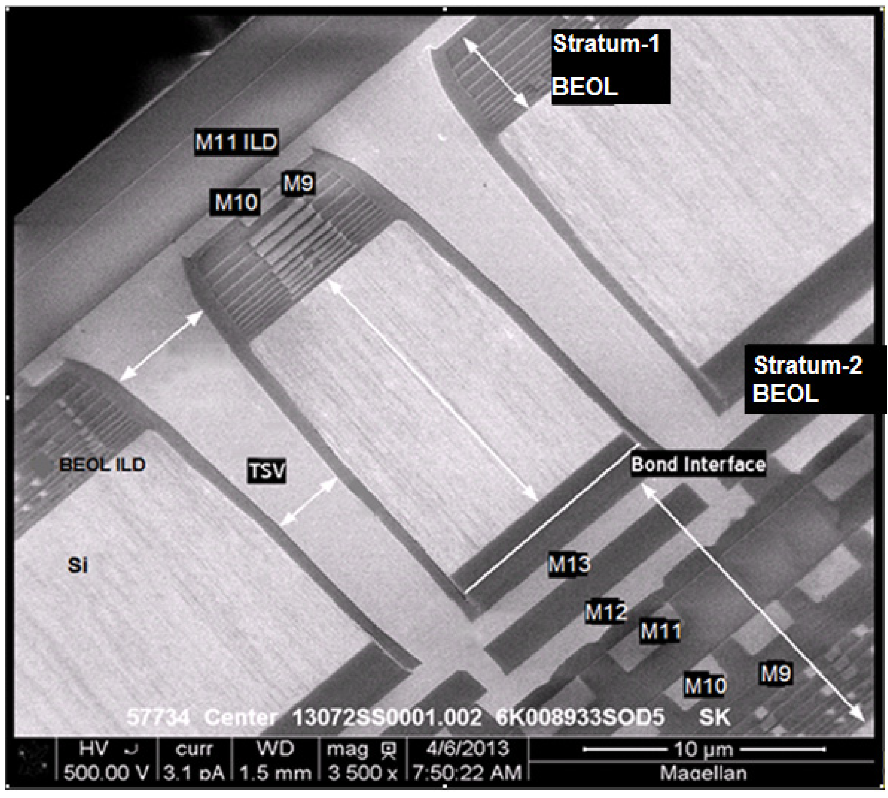
Figure 2.
SEM for stratum-1 and stratum-2 after bonding and removal of handle wafer.
Figure 2.
SEM for stratum-1 and stratum-2 after bonding and removal of handle wafer.
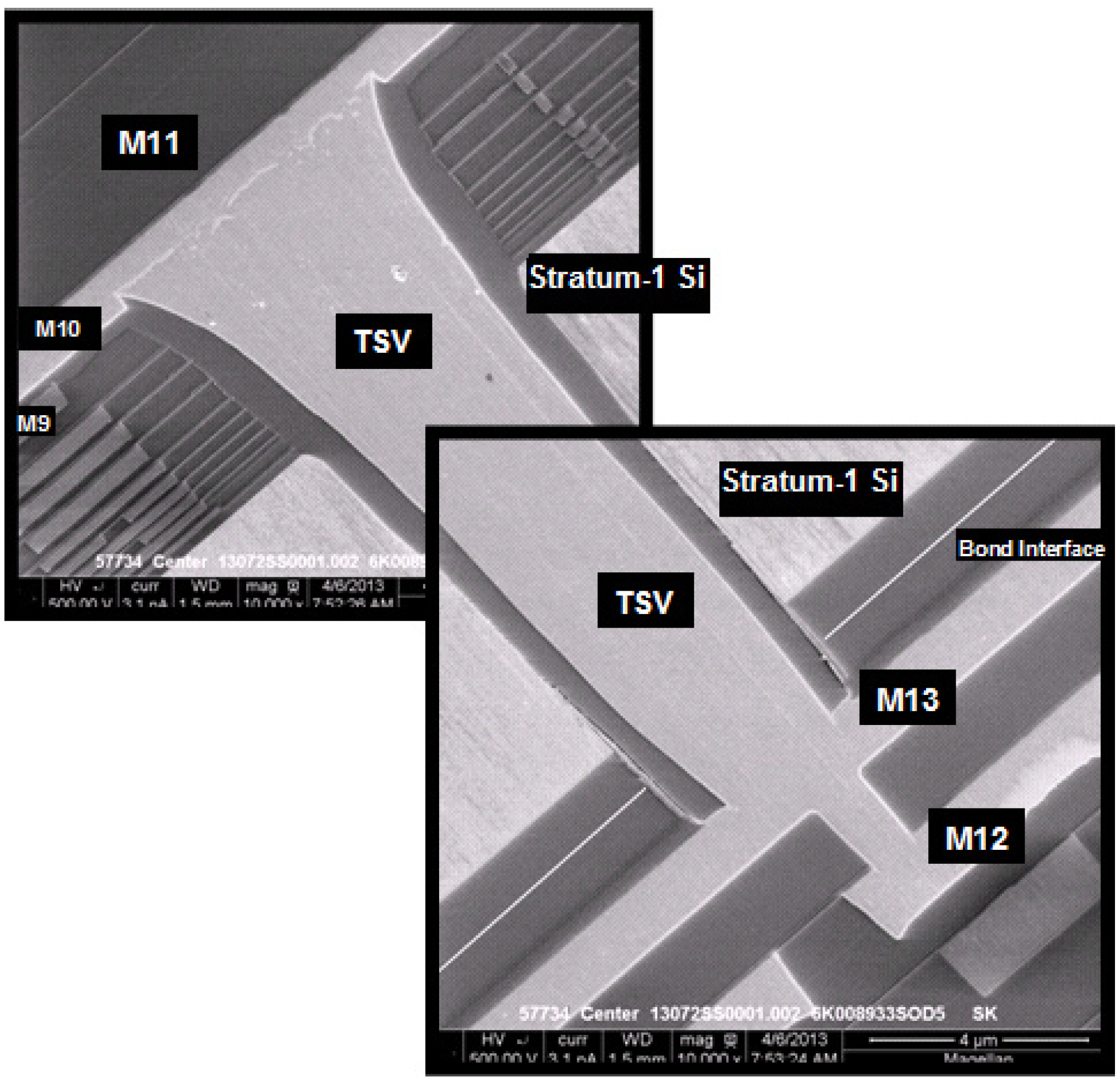
Figure 3.
Cross-section SEM showing integrated TSV and 25 BEOL structures (45 nm).
Figure 3.
Cross-section SEM showing integrated TSV and 25 BEOL structures (45 nm).
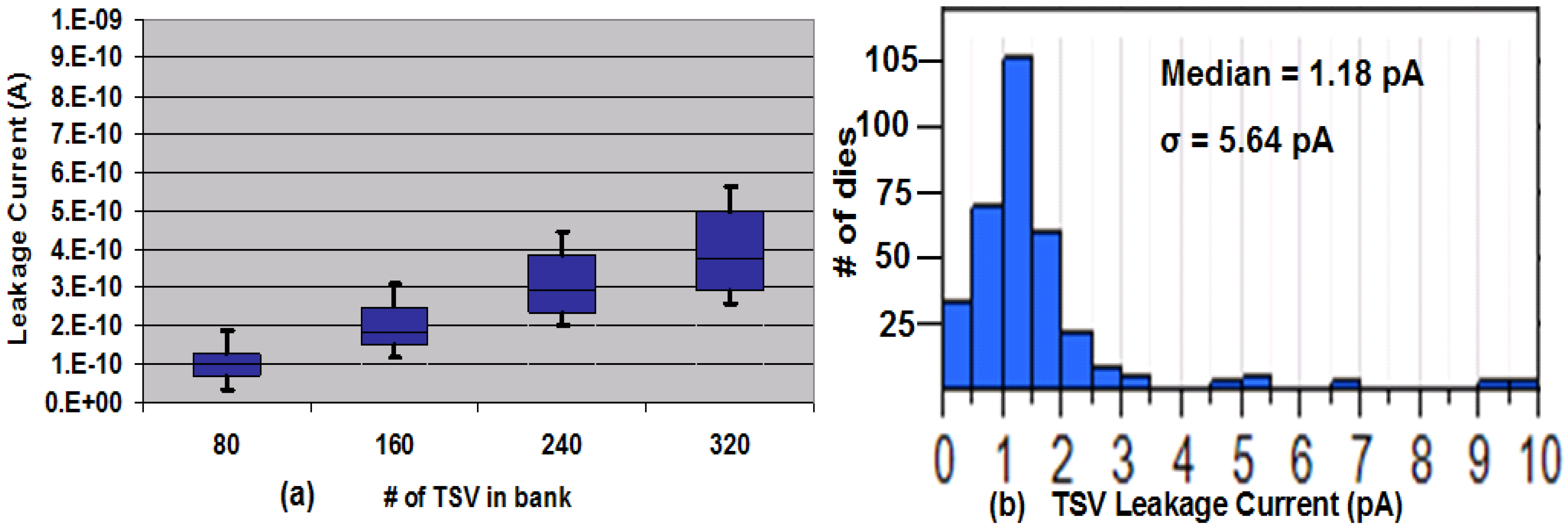
4. Hardware Results
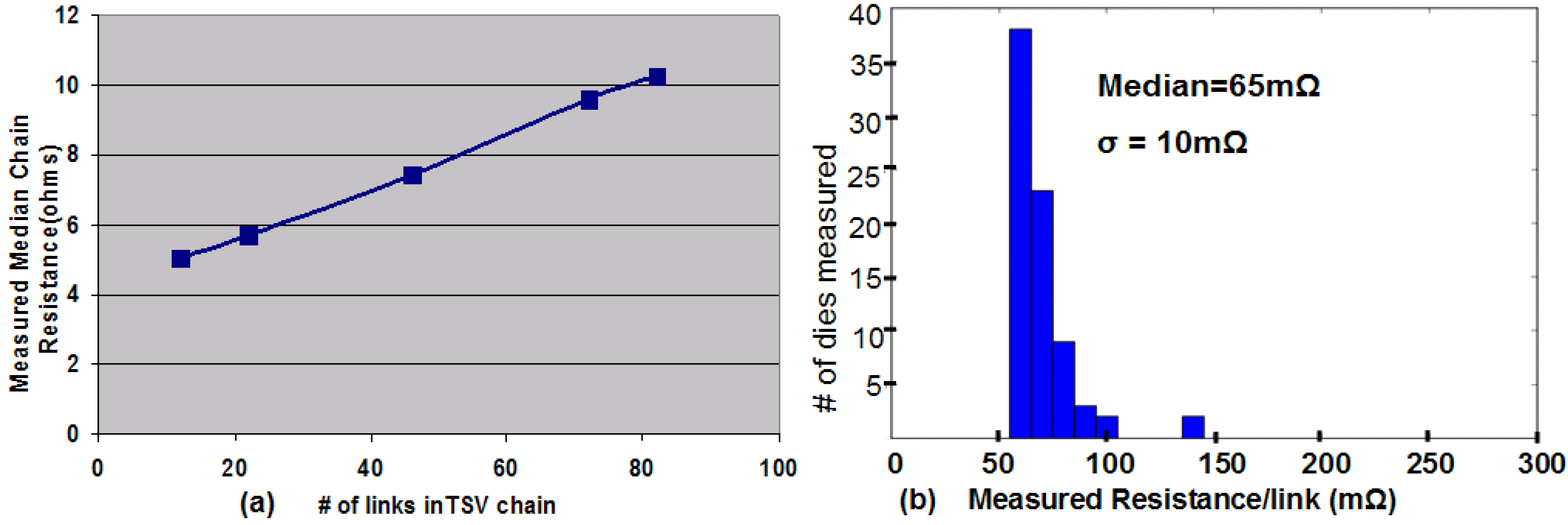
The resistance of TSV chain structures, each link containing two TSVs in parallel, indicates 65 mΩ/link including TSV and local wire resistance (
Figure 4). This can support high performance applications requiring over 1 Amp/mm
2 current density while controlling TSV area penalty under 1%. The measured resistance (
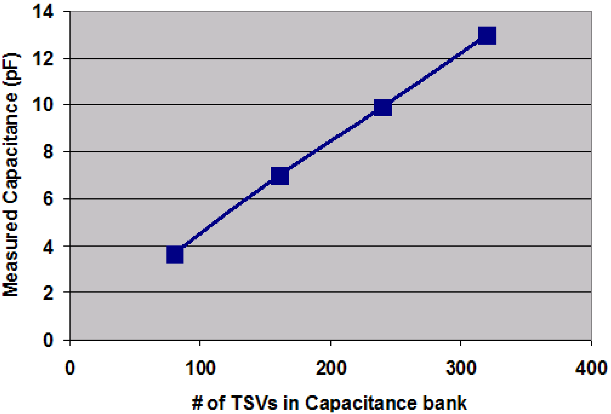
Figure 4b) has standard deviation of 10 mΩ/link indicating a controlled TSV process. TSV capacitance is measured at ~40 fF (
Figure 5) which is <1/4 of the TSV capacitance in bump bond technology [
2,
14]. The TSV RC characteristic is similar to typical 100–200 µm length wiring load enabling 3D macro-to-macro signaling without additional buffering. Capacitance (
Figure 5) and leakage to substrate of TSV arrays (
Figure 6a) modulates with the number of TSVs. The leakage is near the tester limit and extrapolates to 1.18 pA/TSV at 2 V. For a 400 mm
2 chip having up to 50 K TSVs, the total leakage due to TSVs is estimated to be 59 nA (
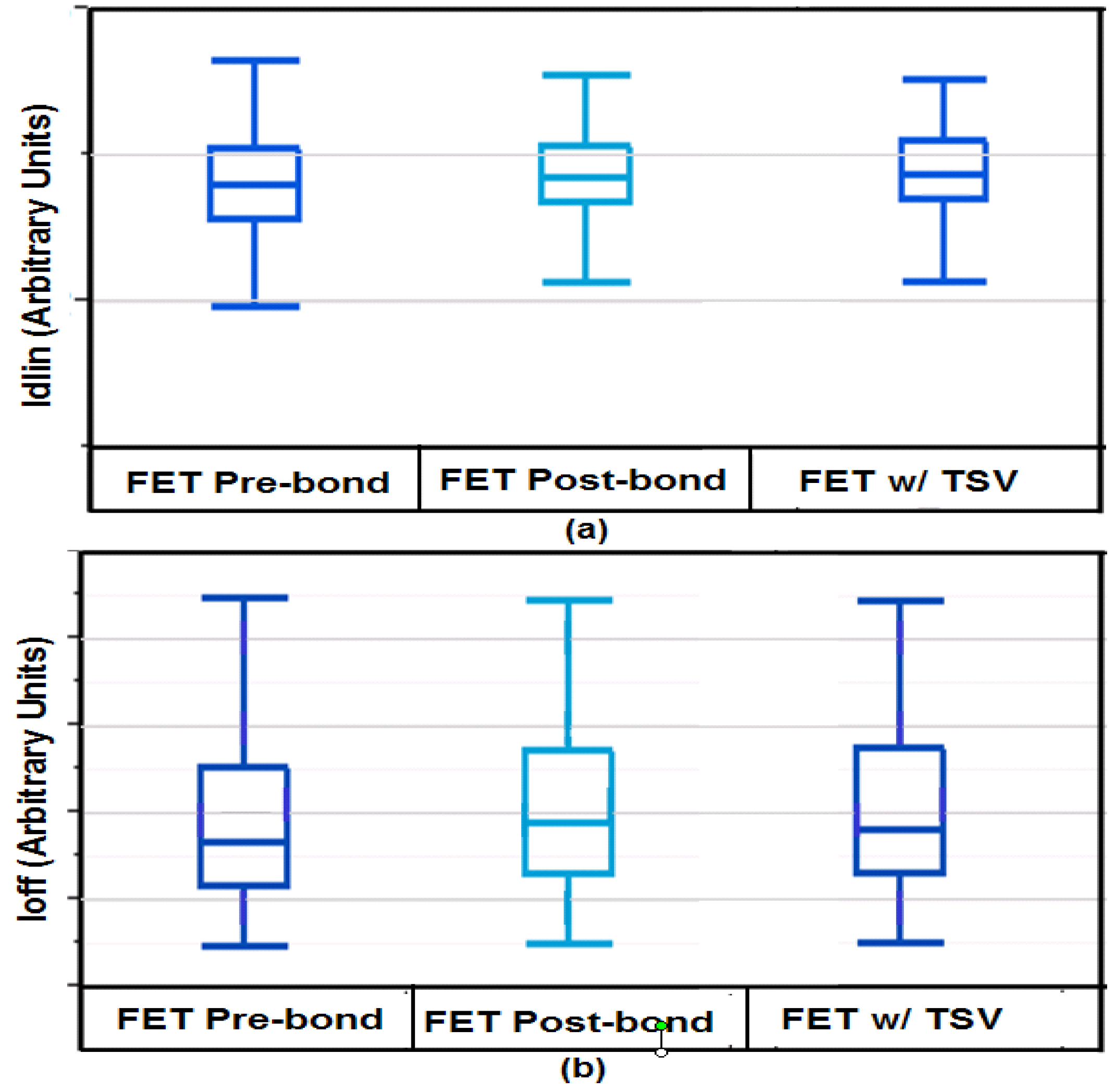
Figure 6b) which is negligible for most applications. FET Ion/Ioff shows no significant change post stacking and TSV processing (
Figure 7).
Figure 4.
(a) Measured TSV chain resistances for lengths of 12, 22, 46, 72, and 82; (b) Distribution of measured resistance/link showing σ = 10 mΩ/link.
Figure 4.
(a) Measured TSV chain resistances for lengths of 12, 22, 46, 72, and 82; (b) Distribution of measured resistance/link showing σ = 10 mΩ/link.
Figure 5.
Capacitance for TSV banks of 80, 160, 240, 320 TSVs.
Figure 5.
Capacitance for TSV banks of 80, 160, 240, 320 TSVs.
Figure 6.
(a) TSV Leakage to substrate at 2 V measured in TSV arrays having 80, 160, 240, 320 TSVs; (b) Distribution of leakage current through each TSV across multiple wafers and dies.
Figure 6.
(a) TSV Leakage to substrate at 2 V measured in TSV arrays having 80, 160, 240, 320 TSVs; (b) Distribution of leakage current through each TSV across multiple wafers and dies.
Figure 7.
PMOS (a) Idlin and (b) Ioff distribution post bonding, thinning and TSV fabrication.
Figure 7.
PMOS (a) Idlin and (b) Ioff distribution post bonding, thinning and TSV fabrication.
As shown in
Figure 7, no significant change in PMOS Idlin and Ioff was observed compared with Ion/Ioff of 2D devices. Pre-bond measurement is done on thick wafers before bonding, post-bond on stratum-1 after bonding before TSV fabrication, and FET with TSV is measured after TSV fabrication on stratum-1. The TSV induced Ion/Ioff variation for NMOS transistors is expected to be smaller than PMOS devices as previously demonstrated [
17,
18] and was not measured for this work.
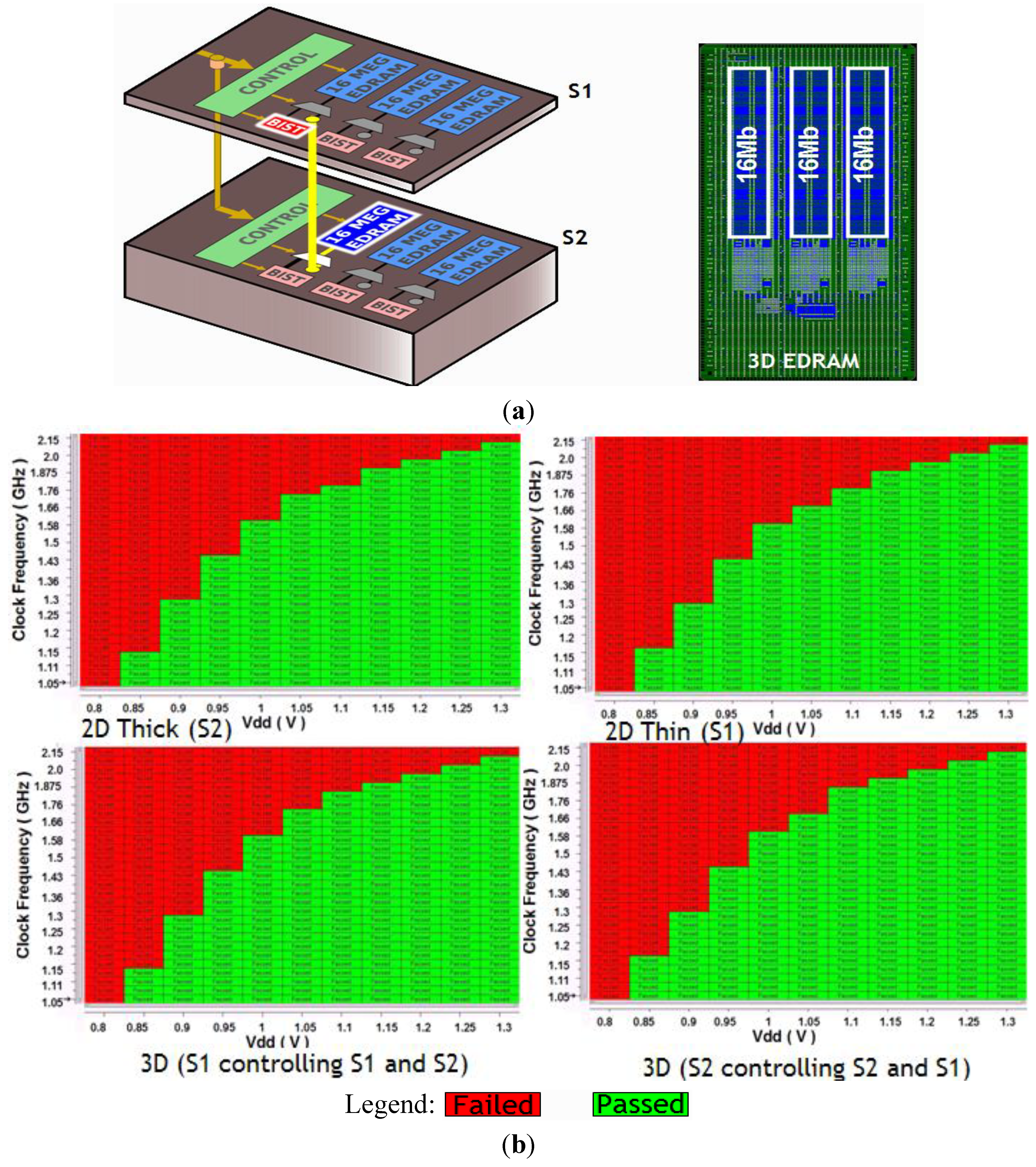
The high-performance stacked EDRAM cache prototype (
Figure 8a) was built using more than 11,000 TSVs. Strata-1 and 2 emulate stacked processor and cache respectively as described in [
5]. Memory functionality and strata-to-strata communication were tested using the built-in-self-test engine (BIST) on each strata. The BIST accessed EDRAM on both strata-1 and 2. The shmoo plot of supply voltage and frequency (
Figure 8b) shows 16 Mb EDRAM functionality (fixable) and strata-to-strata communication up to 2.1 GHz at 1.3 V.
The memory patterns were written in the stacked EDRAM in four different configurations:
- (a)
2D thick wafer mode where the memory on the thick S1 wafer was activated;
- (b)
2D thin wafer mode where the memory on thin wafer S1 was activated and the test patterns were loaded using the TSVs;
- (c)
3D mode where the BIST on S1 controls the memory on S1 as well as S2;
- (d)
3D mode where the BIST on S2 controls the memory on S2 as well as S1.
Modes (c) and (d) demonstrate the ability to write/read data from alternating strata memory in a single cycle thereby confirming the quality of the clocks, power, control and data signals across the chip boundary to be able to transfer the data at speed for entire memory with no errors. Further the shmoo plots in
Figure 8b show that the failure signature in all the modes is very similar indicating that the EDRAM behavior was unaffected by the 3D processing and TSVs. The pattern shmoo was the march9 pattern that forces cycle-to-cycle simultaneous switching patterns across strata boundary. An equivalent column march pattern was also run and the results were similar. The maximum frequency at wafer test was limited by voltage drop inherent with cantilever probing compared to socket based module test. Retention signature of EDRAM indicates a retention time of over 200 µs.
Figure 8.
(a) 3D EDRAM on each wafer comprising 3–16 Mb IP blocks; (b) Shmoo plot showing performance characteristics of wafer-to-wafer stack EDRAM tested with a cantilever wafer probe.
Figure 8.
(a) 3D EDRAM on each wafer comprising 3–16 Mb IP blocks; (b) Shmoo plot showing performance characteristics of wafer-to-wafer stack EDRAM tested with a cantilever wafer probe.
