Ultralow-Power SOTB CMOS Technology Operating Down to 0.4 V †

Abstract
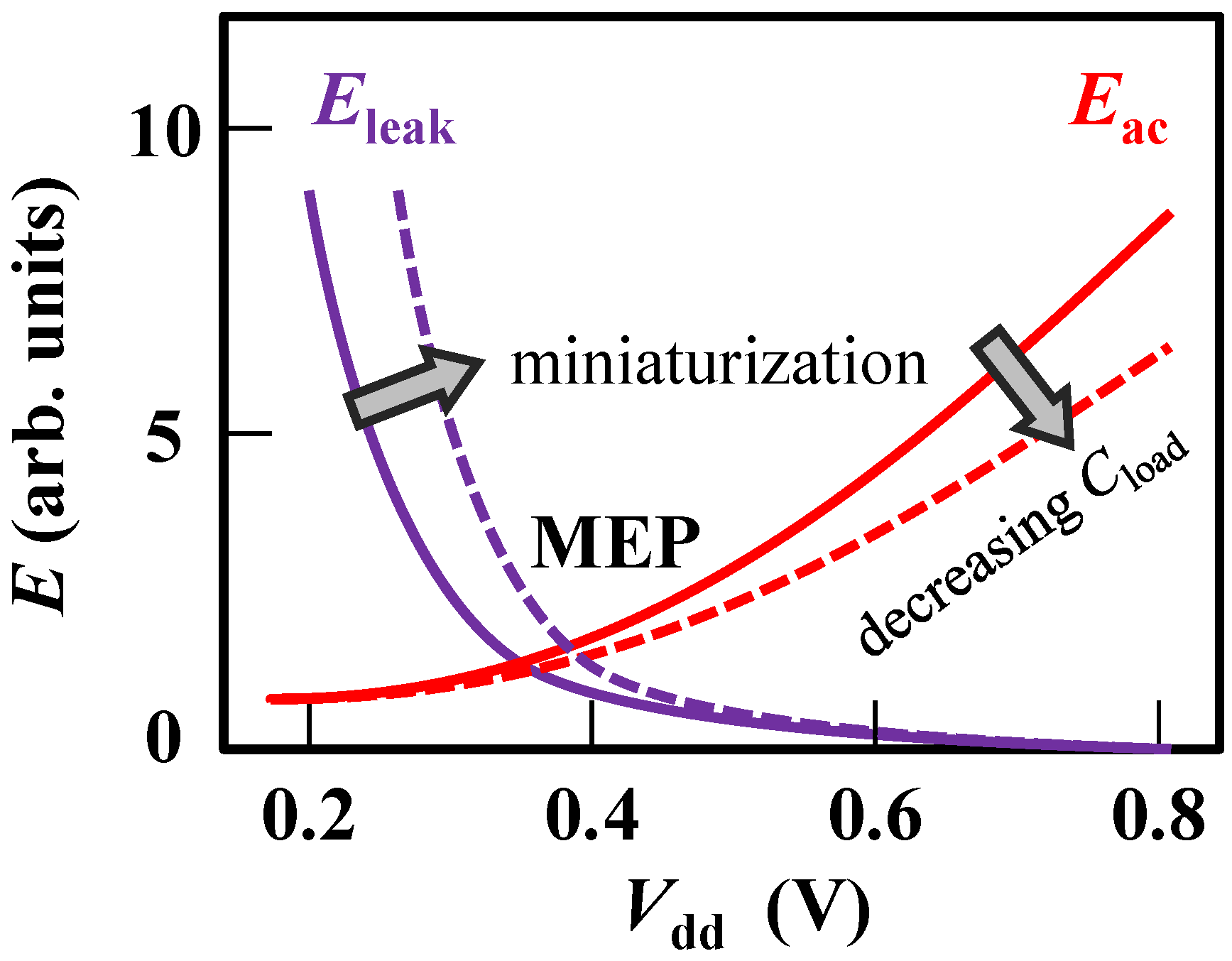
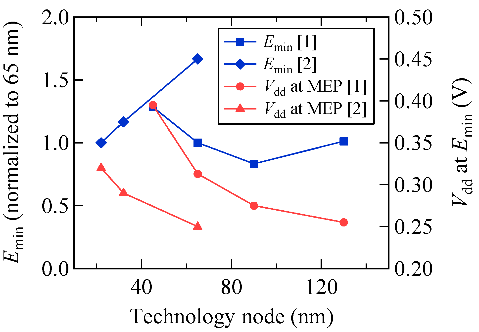
:1. Introduction: Issues for ULV Operation Possibly Staying on MEP Point
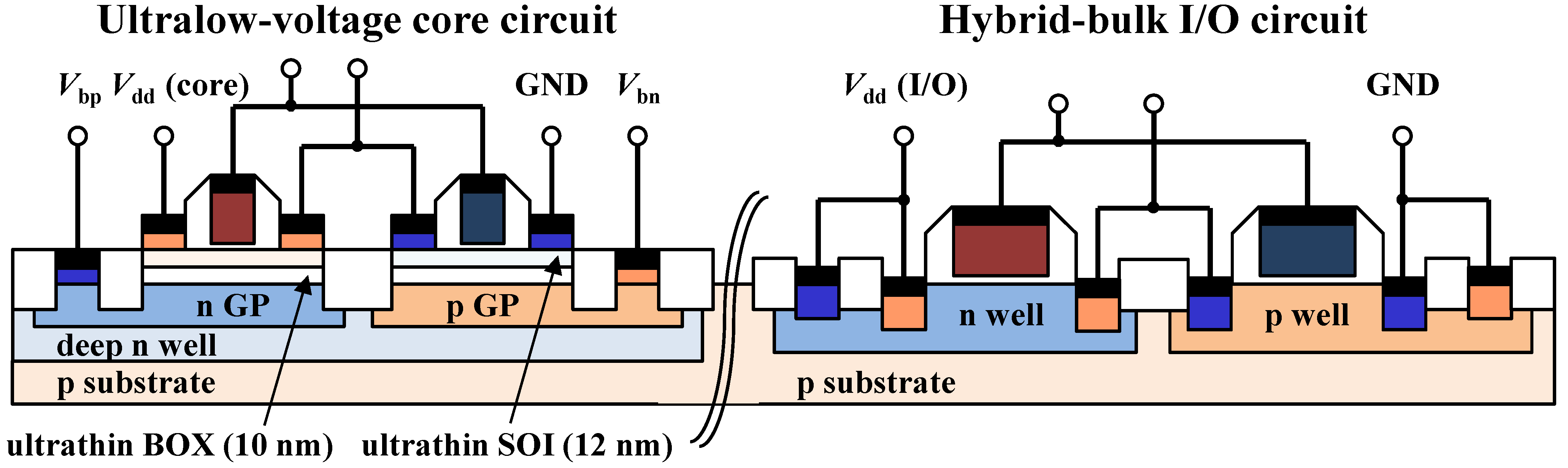
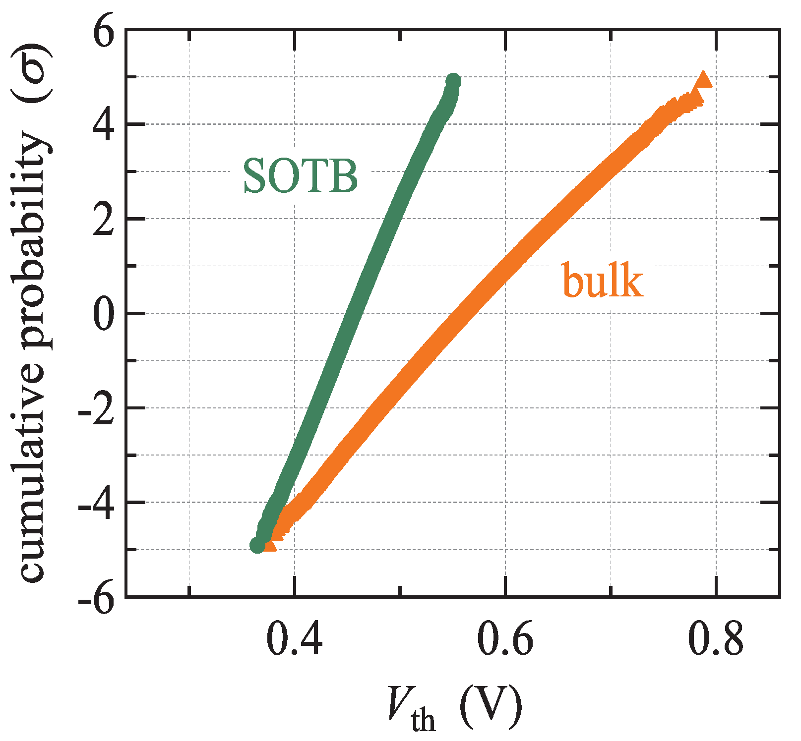
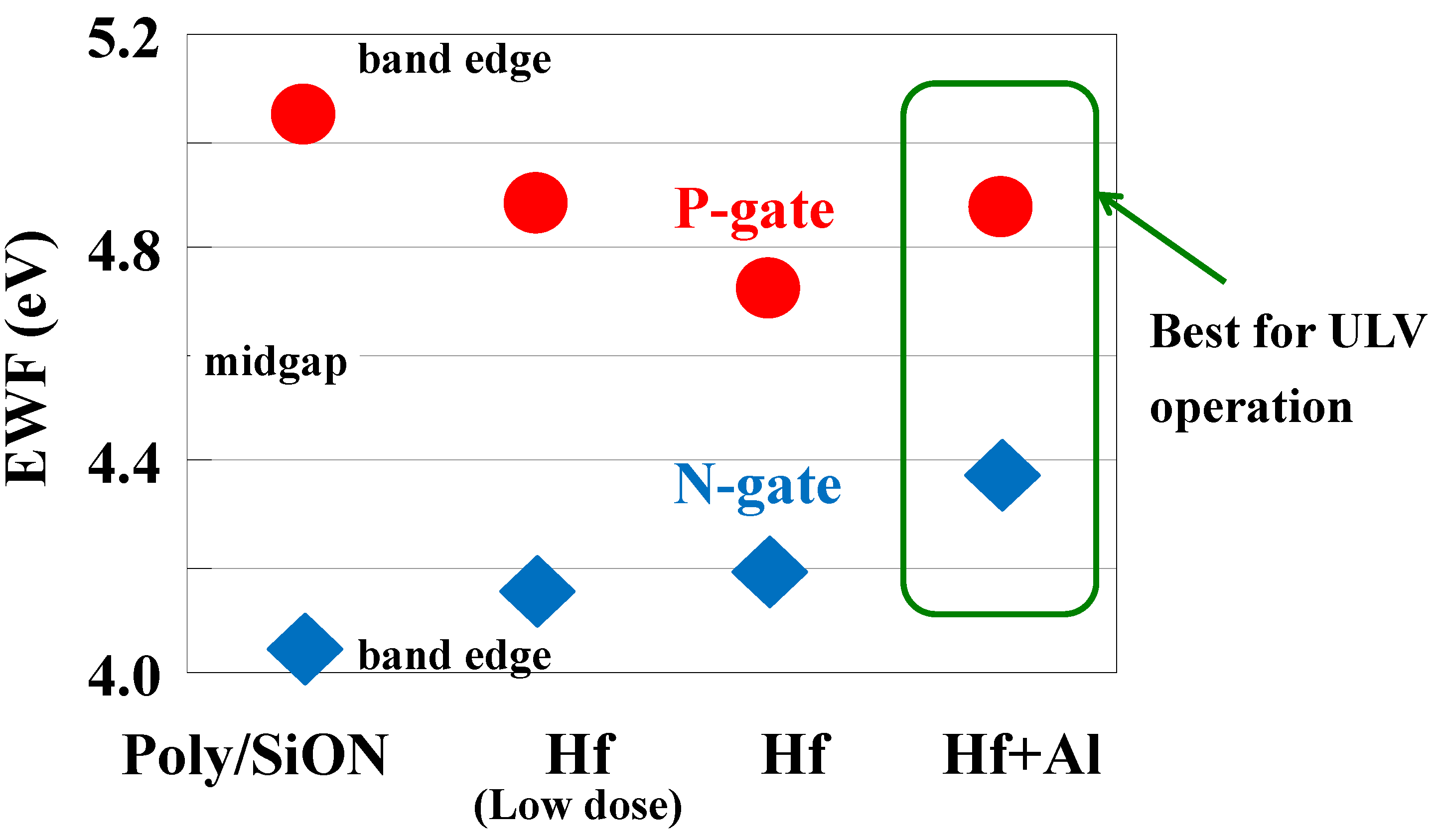
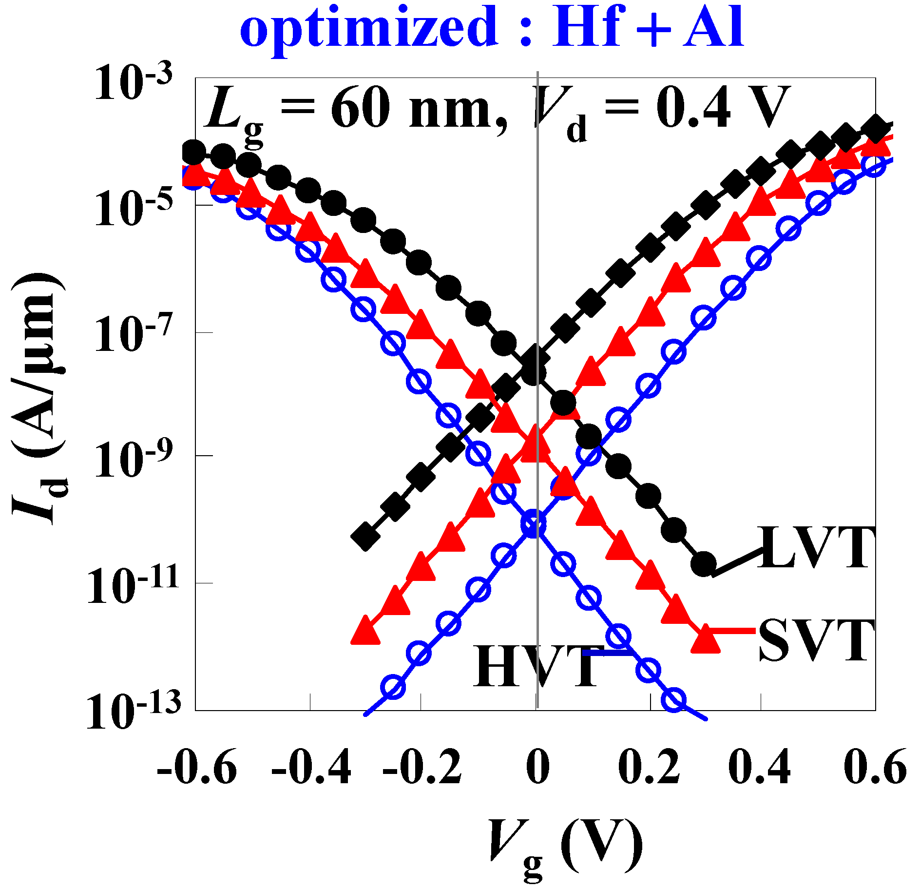
2. SOTB Device Technology


3. ULV Operation of SOTB Circuits
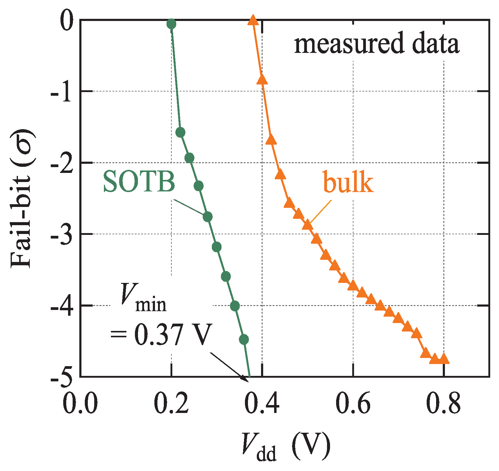
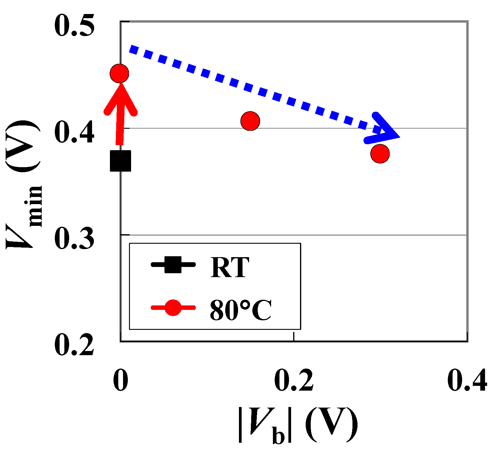
3.1. Vmin Reduction of 6T-SRAM and Leakage Control by Back-Bias
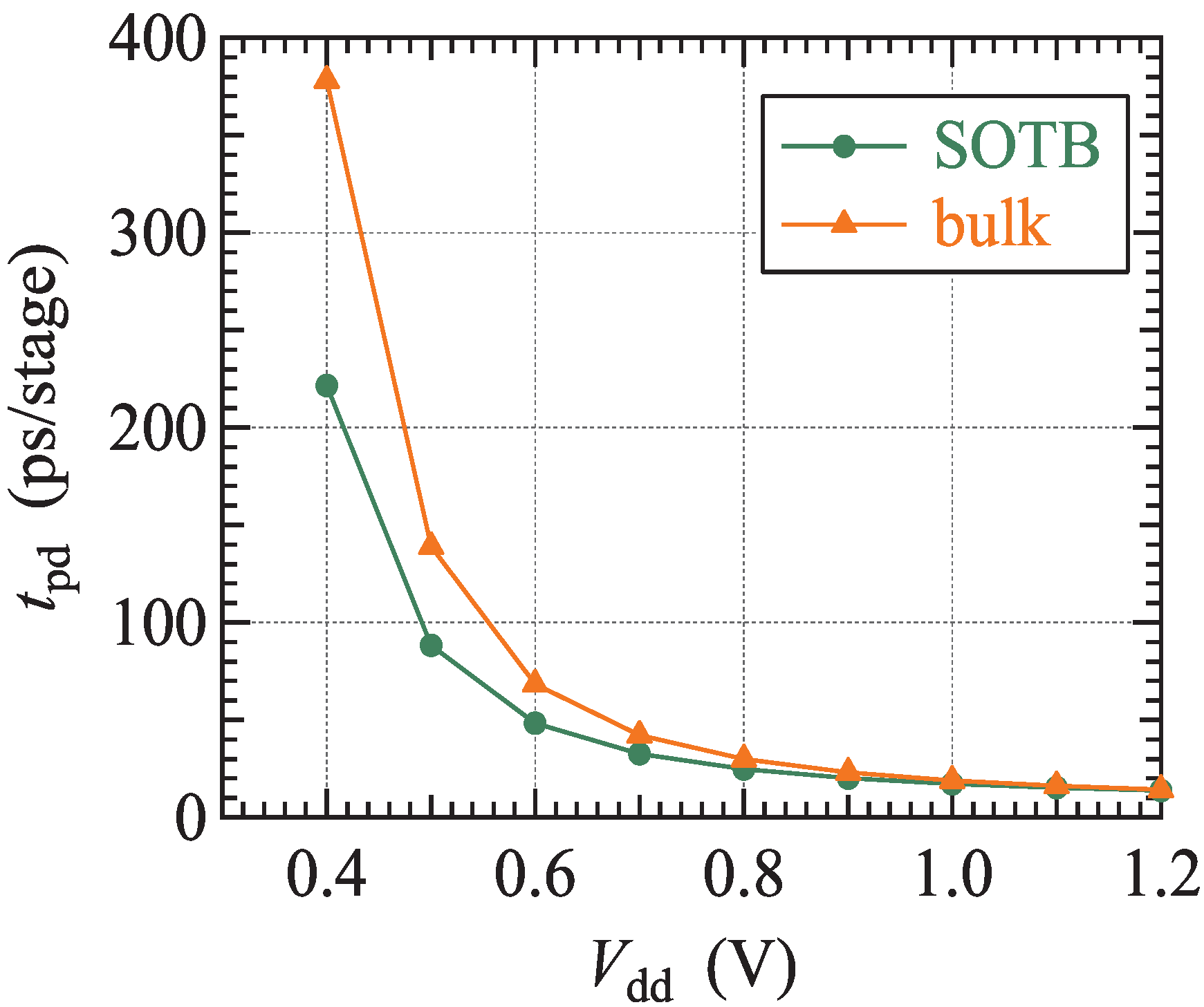
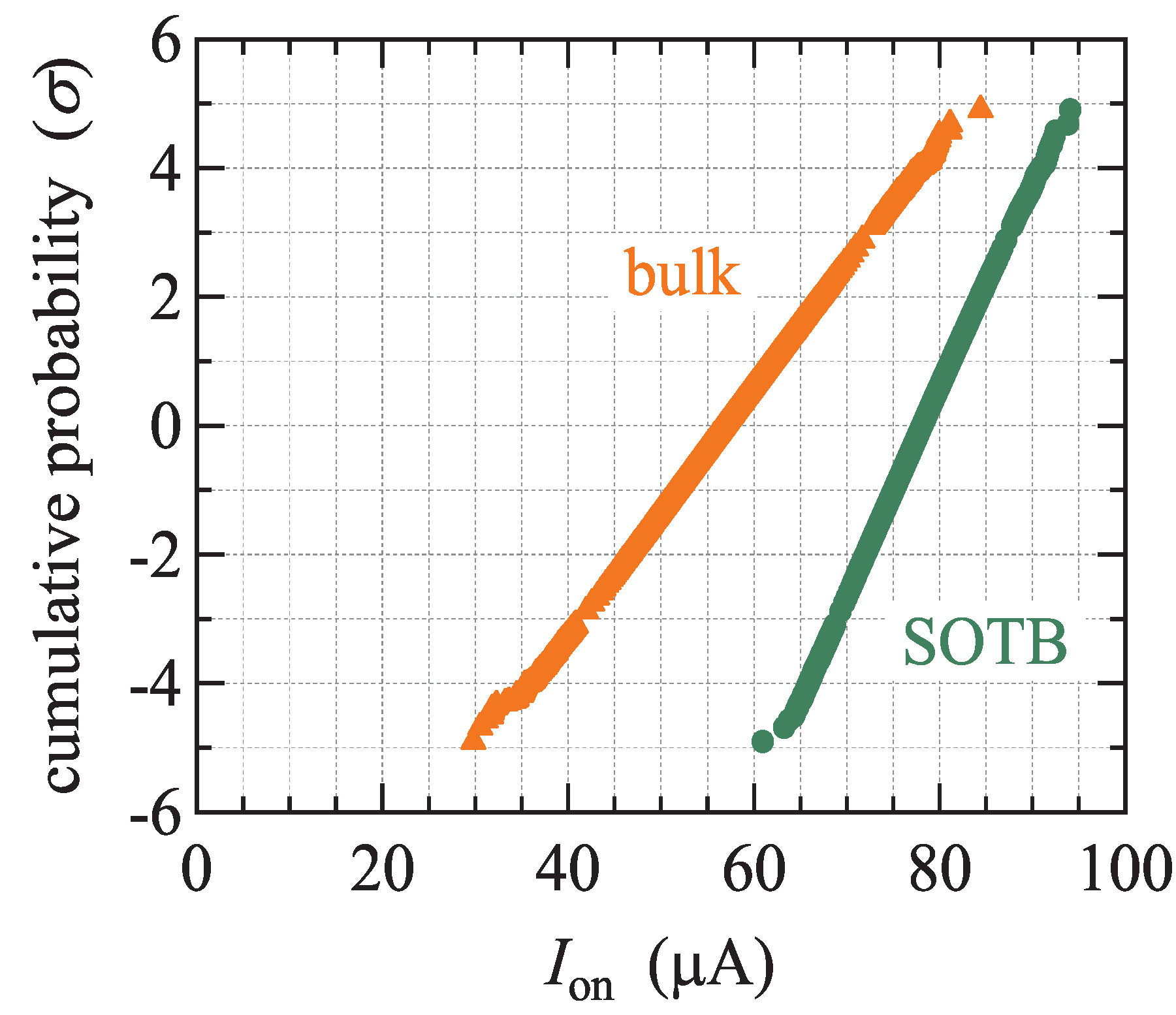
3.2. Ring Oscillator Circuit Results
 dependence. The result means that the local delay variability of SOTB is very small. We also succeeded in the significant reduction of die-to-die delay variability by a proper back-biasing [19]. The logic circuits contain various types of logic cells such as inverter, NAND, NOR, etc. We found that back-biasing considering a drivability balance of NMOS and PMOS transistors is essential for an effective suppression of die-to-die delay variability for various types of the cells.

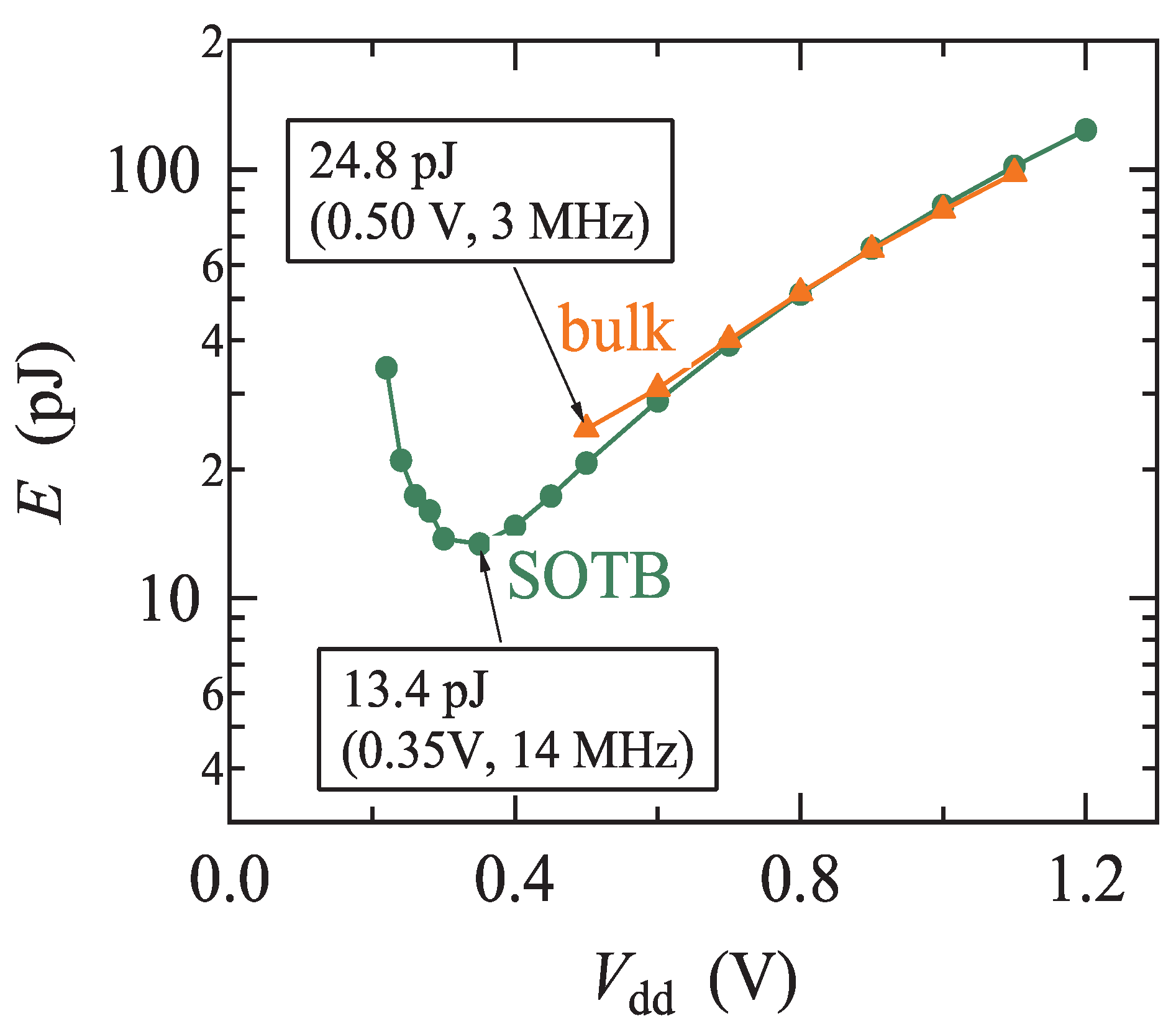
3.3. Demonstration of ULV and ULP Operation of Logic Circuits


4. Conclusions
Acknowledgments
Author Contributions
Conflicts of Interest
References
- Bol, D.; Kamel, D.; Flandre, D.; Legat, J.-D. Nanometer MOSFET Effects on the Minimum-Energy Point of 45nm Subthreshold Logic. In Proceedings of the 14th IEEE/ACM International Symposium on Low-Power Electronics and Design, San Franciscon, CA, USA, 19–21 August 2009; pp. 3–8.
- Chandrakasan, A.P.; Daly, D.C.; Finchelstein, D.C.; Kwong, J.; Ramadass, Y.K.; Sinangil, M.E.; Sze, V.; Vermaet, N. Technologies for ultradynamic voltage scaling. Proc. IEEE 2010, 98, 191–214. [Google Scholar] [CrossRef]
- Zhai, B.; Nazhandali, L.; Olson, J.; Reeves, A.; Minuth, M.; Helfand, R.; Pant, S.; Blaauw, D.; Austin, T. A 2.60 pJ/Inst Subthreshold Sensor Processor for Optimal Energy Efficiency. In Proceedings of the 2006 Symposium on VLSI CircuitsDigest of Technical Papers, Honolulu, HI, USA, 15–17 June 2006; pp. 154–155.
- Wang, A.; Chandrakasan, A. A 180-mV subthreshold FFT processor using a minimum energy design methodology. IEEE J. Solid-State Circuits 2005, 40, 310–319. [Google Scholar] [CrossRef]
- Slimani, M.; Silveira, F.; Matherat, P. Variability-Speed-Consumption Trade-off in Near Threshold Operation. In Proceedings of the 21st The International Workshop on Power and Timing Modeling, Optimization and Simulation (PATMOS), Madrid, Spain, 26–29 September 2011; pp. 308–316. [CrossRef]
- Sugii, N.; Tsuchiya, R.; Ishigaki, T.; Morita, Y.; Yoshimoto, H.; Iwamatsu, T.; Oda, H.; Inoue, Y.; Hiramoto, T.; Kimura, S. Evaluation of threshold-voltage variation in silicon on thin buried oxide complementary metal–oxide–semiconductor and its impact on decreasing standby leakage current. Jpn. J. Appl. Phys. 2009, 48, 04C043. [Google Scholar]
- Seo, S.; Dreslinski, R.G.; Woh, M.; Park, J.; Charkrabari, C.; Mahlke, S.; Blaauw, D.; Mudge, T. Process Variation in Near-Threshold Wide SIMD Architectures. In Proceedings of the 49th ACM/EDAC/IEEE Design Automation Conference (DAC), San Francisco, CA, USA, 3–7 June 2012; pp. 980–987.
- Kwong, J.; Chandrakasan, A.P. Variation-Driven Device Sizing for Minimum Energy Sub-Threshold Circuits. In Proceedings of the 2006 International Symposium on Low Power Electronics and Design (ISLPED’06), Tegernsee, Germany, 4–6 October 2006; pp. 8–13.
- Blaauw, D.; Zhai, B. Energy Efficient Design for Subthreshold Supply Voltage Operation. In Proceedings of the 2006 IEEE International Symposium on Circuits and Systems (ISCAS) 2006, Island of Kos, Greece, 21–24 May 2006; p. 32.
- Bowman, K.A.; Duvall, S.G.; Meindl, J.D. Impact of Die-to-Die and within-Die Parameter Fluctuations on the Maximum Clock Frequency Distribution. In Proceedings of the 2001 IEEE International Solid-State Circuits Conference (ISSCC), Digest of Technical Papers 2001, San Francisco, CA, USA, 7 February 2001; pp. 278–279.
- Datta, A.; Bhunia, S.; Mukhopadhyay, S.; Roy, K. Delay modeling and statistical design of pipelined circuit under process variation. IEEE Trans. Comput. Aided Des. Integr. Circuits Syst. 2006, 25, 2427–2436. [Google Scholar] [CrossRef]
- Tsuchiya, R.; Horiuchi, M.; Kimura, S.; Yamaoka, M.; Kawahara, T.; Maegawa, S.; Ipposhi, T.; Ohji, Y.; Matsuoka, H. Silicon on Thin BOX: A New Paradigm of the CMOSFET for Low-Power High-Performance Application Featuring Wide-Range Back-Bias Control. In Proceedings of the IEEE International Electron Devices Meeting, IEDM Technical Digest, San Francisco, CA, USA, 13–15 December 2004; pp. 631–634.
- Morita, Y.; Tsuchiya, R.; Ishigaki, T.; Sugii, N.; Iwamatsu, T.; Ipposhi, T.; Oda, H.; Inoue, Y.; Torii, K.; Kimura, S. Smallest Vth Variability Achieved by Intrinsic Silicon on Thin BOX (SOTB) CMOS with Single Metal Gate. In Proceedings of the 2008 Symposium on VLSI Technology, Honolulu, HI, USA, 17–19 June 2008; pp. 166–167.
- Sugii, N.; Tsuchiya, R.; Ishigaki, T.; Morita, Y.; Yoshimoto, H.; Kimura, S. Local Vth variability and scalability in Silicon-on-Thin-BOX (SOTB) CMOS with small random-dopant fluctuation. IEEE Trans. Electron Devices 2010, 57, 835–845. [Google Scholar] [CrossRef]
- Yamamoto, Y.; Makiyama, H.; Tsunomura, T.; Iwamatsu, T.; Oda, H.; Sugii, N.; Yamaguchi, Y.; Mizutani, T.; Hiramoto, T. Poly/high-k/SiON Gate Stack and Novel Profile Engineering Dedicated for Ultralow-Voltage Silicon-on-Thin-BOX (SOTB) CMOS Operation. In Proceedings of the 2012 Symposium on VLSI Technology, Honolulu, HI, USA, 12–14 June 2012; pp. 109–110.
- Yamamoto, Y.; Makiyama, H.; Shinohara, H.; Iwamatsu, T.; Oda, H.; Kamohara, S.; Sugii, N.; Yamaguchi, Y.; Mizutani, T.; Hiramoto, T. Ultralow-Voltage Operation of Silicon-on-Thin-BOX (SOTB) 2 Mbit SRAM Down to 0.37 V Utilizing Adaptive Back Bias. In Proceedings of the 2013 Symposium on VLSI Technology, Kyoto, Japan, 11–13 June 2013; pp. T212–T213.
- Mizutani, T.; Yamamoto, Y.; Makiyama, H.; Tsunomura, T.; Iwamatsu, T.; Oda, H.; Sugii, N.; Hiramoto, T. Reduced Drain Current Variability in Fully Depleted Silicon-on-Thin-BOX (SOTB) MOSFETs. In Proceedings of the 2012 IEEE Silicon Nanoelectronics Workshop (SNW), Honolulu, HI, USA, 10–11 June 2012; pp. 1–2.
- Makiyama, H.; Yamamoto, Y.; Shinohara, H.; Iwamatsu, T.; Oda, H.; Sugii, N.; Ishibashi, K.; Yamaguchi, Y. Speed enhancement at Vdd = 0.4 V and random τpd variability reduction and analyisis of τpd variability of silicon on thin buried oxide circuits. Jpn. J. Appl. Phys. 2014, 53. [Google Scholar] [CrossRef]
- Makiyama, H.; Yamamoto, Y.; Shinohara, H.; Iwamatsu, T.; Oda, H.; Sugii, N.; Ishibashi, K.; Mizutani, T.; Hiramoto, T.; Yamaguchi, Y. Suppression of Die-to-Die Delay Variability of Silicon on Thin Buried Oxide (SOTB) CMOS Circuits by Balanced P/N Drivability Control with Back-Bias for Ultralow-Voltage (0.4 V) Operation. In Proceedings of the 2013 IEEE International Electron Devices Meeting (IEDM), Washington, DC, USA, 9–11 December 2013; pp. 822–825.
- Morohashi, S.; Sugii, N.; Iwamatsu, T.; Kamohara, S.; Kato, Y.; Pham, C.-K.; Ishibashi, K. A 44 μW/10 MHz Minimum Power Operation of 50 K Logic Gate Using 65 nm SOTB Devices with Back Gate Control. In Proceedings of the 2013 IEEE SOI-3D-Subthreshold Microelectronics Technology Unified Conference (S3S), Monterey, CA, USA, 7–10 October 2013; pp. 165–166.
- Su, H.; Amano, H. Real Chip Evaluation of a Low Power Reconfigurable Accelerator with SOTB Technology; Technical Report of The Institute of Electronics, Information and Communication Engineers (IEICE), RECONF2013-52; IEICE: Tokyo, Japan, 2013; Volume 113, pp. 71–76. (In Japanese) [Google Scholar]
- Hioki, M.; Ma, C.; Kawanami, T.; Ogasahara, Y.; Nakagawa, T.; Sekigawa, T.; Tsutsumi, T.; Koike, H. The First SOTB Implementation of Flex Power FPGA. J. Low Power Electron. Appl. Submitted.
- Nagatomi, H.; Le, D.-H.; Pham, C.-K.; Sugii, N.; Kamohara, S.; Iwamatsu, T.; Ishibashi, K. A 4 pA/Gate Sleep Current 65 nm SOTB Logic Gates Using On-chip VBB Generator for Energy Harvesting Sensor Network Systems. In Proceedings of the 2013 International Conference on Integrated Circuits, Design, and Verification (ICDV 2013), Ho Chi Minh City, Vietnam, 15–16 November 2013.
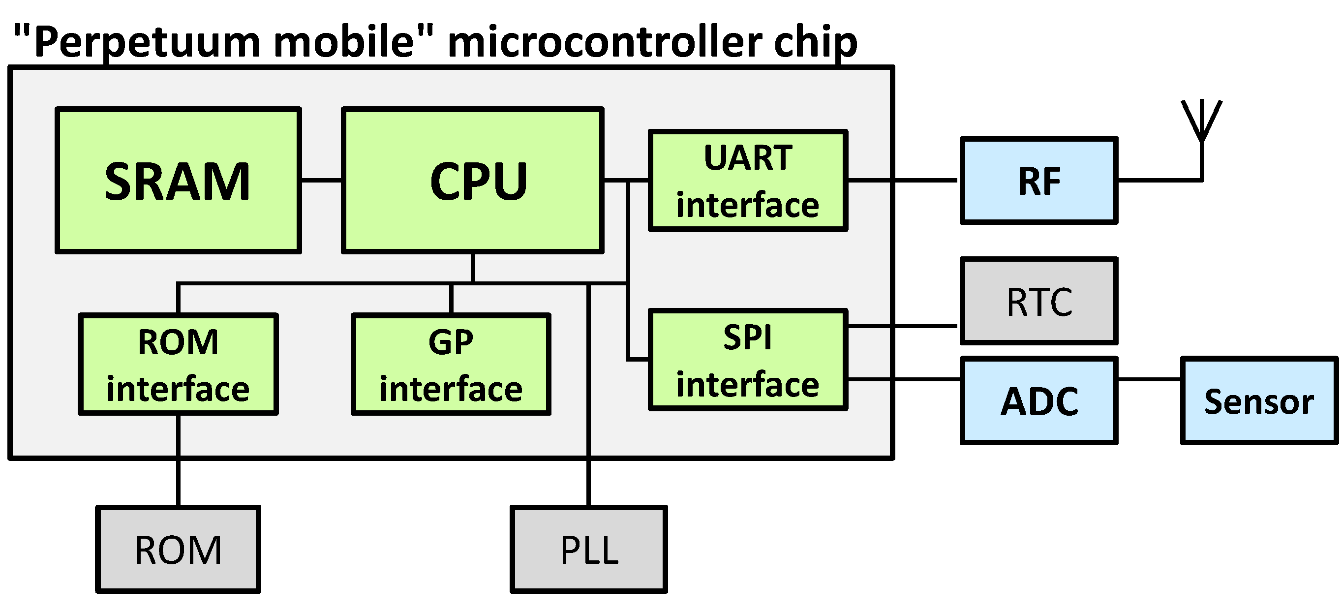
- Ishibashi, K.; Sugii, N.; Usami, K.; Amano, H.; Kobayashi, K.; Pham, C.-K.; Makiyama, H.; Yamamoto, Y.; Shinohara, H.; Iwamatsu, T.; et al. A Perpetuum Mobile 32 bit CPU with 13.4 pJ/cycle, 0.14 µA Sleep Current using Reverse Body Bias Assisted 65 nm SOTB CMOS Technology. In Proceedings of the COOL Chips XVII, Yokohama, Kanagawa, Japan, 14–16 April 2014.
© 2014 by the authors; licensee MDPI, Basel, Switzerland. This article is an open access article distributed under the terms and conditions of the Creative Commons Attribution license (http://creativecommons.org/licenses/by/3.0/).
Share and Cite
Sugii, N.; Yamamoto, Y.; Makiyama, H.; Yamashita, T.; Oda, H.; Kamohara, S.; Yamaguchi, Y.; Ishibashi, K.; Mizutani, T.; Hiramoto, T. Ultralow-Power SOTB CMOS Technology Operating Down to 0.4 V. J. Low Power Electron. Appl. 2014, 4, 65-76. https://doi.org/10.3390/jlpea4020065
Sugii N, Yamamoto Y, Makiyama H, Yamashita T, Oda H, Kamohara S, Yamaguchi Y, Ishibashi K, Mizutani T, Hiramoto T. Ultralow-Power SOTB CMOS Technology Operating Down to 0.4 V. Journal of Low Power Electronics and Applications. 2014; 4(2):65-76. https://doi.org/10.3390/jlpea4020065
Chicago/Turabian StyleSugii, Nobuyuki, Yoshiki Yamamoto, Hideki Makiyama, Tomohiro Yamashita, Hidekazu Oda, Shiro Kamohara, Yasuo Yamaguchi, Koichiro Ishibashi, Tomoko Mizutani, and Toshiro Hiramoto. 2014. "Ultralow-Power SOTB CMOS Technology Operating Down to 0.4 V" Journal of Low Power Electronics and Applications 4, no. 2: 65-76. https://doi.org/10.3390/jlpea4020065
APA StyleSugii, N., Yamamoto, Y., Makiyama, H., Yamashita, T., Oda, H., Kamohara, S., Yamaguchi, Y., Ishibashi, K., Mizutani, T., & Hiramoto, T. (2014). Ultralow-Power SOTB CMOS Technology Operating Down to 0.4 V. Journal of Low Power Electronics and Applications, 4(2), 65-76. https://doi.org/10.3390/jlpea4020065