1. Introduction
Adiabatic logic circuits were introduced as a possible means to achieve ultra-low power circuits by taking advantage of the adiabatic charging principle [
1,
2,
3,
4] (the adiabatic charging principle states that if the voltage in a circuit changes slower than the electric time constant of the circuit, then resistive losses are reduced). However, while the adiabatic charging principle affords a possibly unlimited energy-performance compromise [
3], at least in theory, the fact is that CMOS-based adiabatic circuits suffer from non-adiabatic residues and leakage loss components that deteriorate their performance.
On the other hand, electrostatic nanoelectromechanical (NEM) switches have already been suggested and demonstrated for use in classical logic circuits [
5,
6,
7,
8]. NEM switches offer the advantage of zero leakage current and therefore zero static power dissipation, which is an appealing property for low power low performance circuits. However, these switches require high operating voltages and suffer from low switching speeds when compared to MOSFETs, see for example [
5] and [
7] for a comprehensive review. These factors constitute serious obstacles to replace CMOS circuits by NEM relays for low power solution.
Nonetheless, NEM switches are ideal candidates to replace classical CMOS elements in adiabatic logic circuits [
9], where the zero leakage current experienced in NEM switches allows the efficient operation of NEM-based adiabatic logic circuits at low frequencies without any static dissipation penalties, and at the same time the use of adiabatic charging makes it possible to offset the high energy dissipation that accompanies the voltages required to operate the nanoelectromechamical relays.
In this paper, the basic principles of adiabatic circuits will be presented, the dissipation of adiabatic circuits will be explicitly derived based on a simplified circuit model and compared for three different device technologies, which are: the classical CMOS-based circuit, the sub-threshold CMOS-based circuit and NEMS-based circuit respectively. It will be shown that replacing a MOSFET switch by an ideal electromechanical one does contribute in reducing significantly the power dissipation. It will also be demonstrated that the contact resistance of electromechanical switches may well be a limiting factor on the performance of NEM-based adiabatic logic circuits. This paper aims to present a modeling based results that gives to a good approximation the qualitative behavior of NEMS-based adiabatic logic circuits.
This paper starts by introducing the principle of adiabatic charging and how it translates to energy saving in logic circuits in
Section 2. The energy saving terms will be derived for both CMOS, and sub-threshold CMOS in
Section 3. Afterwards, electrostatic nanoelectromechanical relays will be introduced in
Section 4, and attention will be given to the contact resistance of NEM switches, followed by an explicit derivation of the performance limits of NEM-based adiabatic circuits. A brief discussion of the results will be given in
Section 5. Finally, the paper ends by a discussion regarding the implication of obtained results for circuit design and possible future trends in
Section 6.
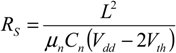
2. Adiabatic Charging of an RC Circuit
The operation of a logic circuit typically consists of charging a capacitor through a series resistance, where the capacitor is mainly that of the fan out interconnect and the resistance is dominated by the switching element series resistance.
In conventional circuits, the capacitor charging is done under constant voltage, which is the circuit operating voltage
Vdd. This constant voltage charging results in dissipative energy losses of
![Jlpea 03 00368 i021]()
for a charge-discharge cycle. This remains the case regardless of the values of the series resistance or load capacitance.
In adiabatic charging, a slowly varying voltage source, usually a linearly ramped voltage, is used to charge and discharge the load capacitance [
10]. This slowly varying voltage source results in a reduced dissipated energy
E for the charge-discharge cycle given by:
where
R is the series resistance assumed to be dominated by the switching element,
C is the load capacitance, and
T is the ramp period. Equation (1) is accurate while
![Jlpea 03 00368 i022]()
.
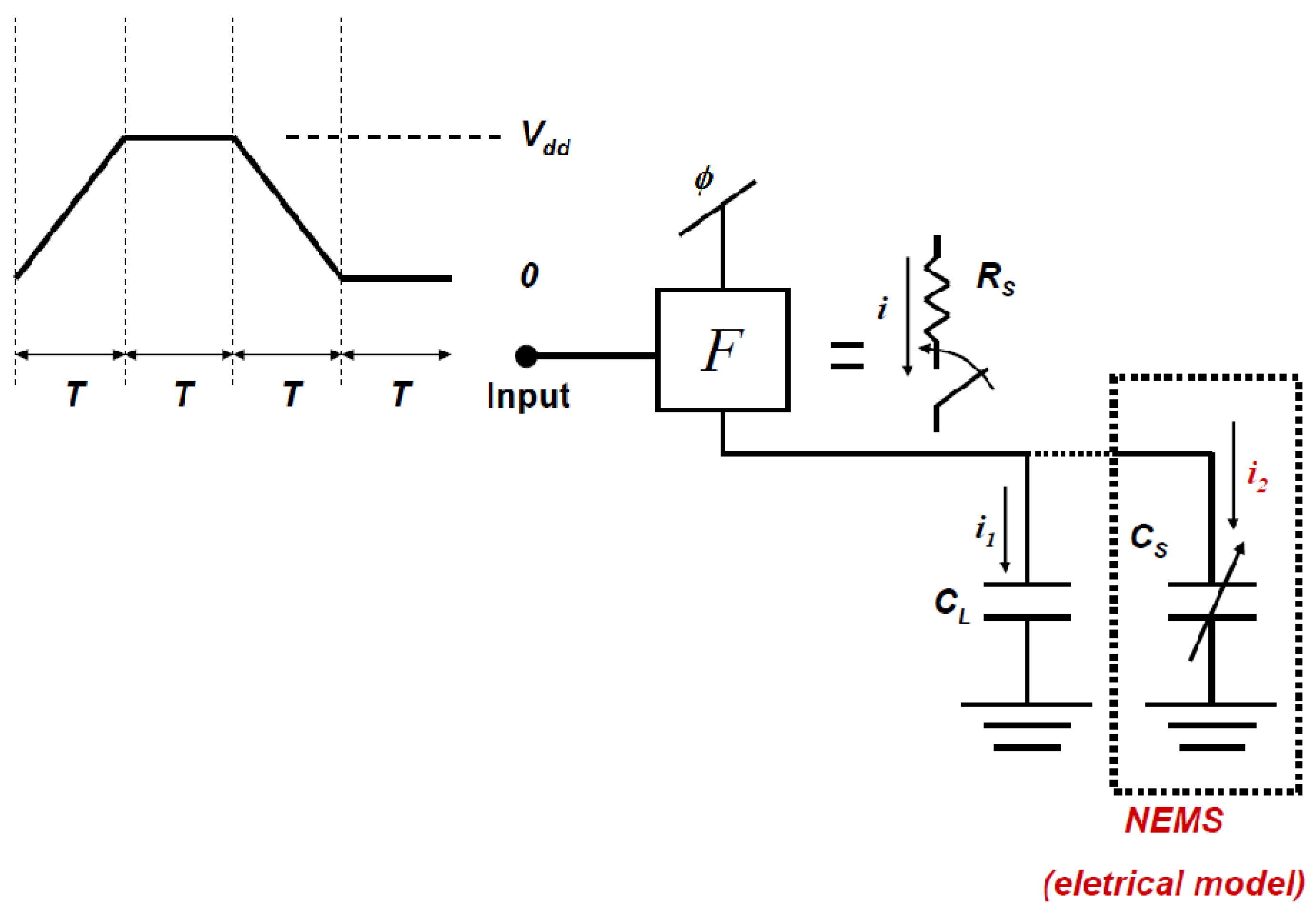
A simplified model of a typical adiabatic logic circuit is schematically represented in
Figure 1, showing both the series resistance and the load capacitance. In the case of a NEMS switch, a variable capacitance
CS is added to represent the change in the NEMS device capacitance upon commutation (the origin of this change in capacitance will be detailed in
Section 4). Also shown is the typical four-phase power clock (
ϕ) used, where the ramp-up, hold, and the ramp-down times are shown each having a period
T. In a typical adiabatic circuit, both the power clock and the input have the same waveform with a
T phase shift between the two [
4].
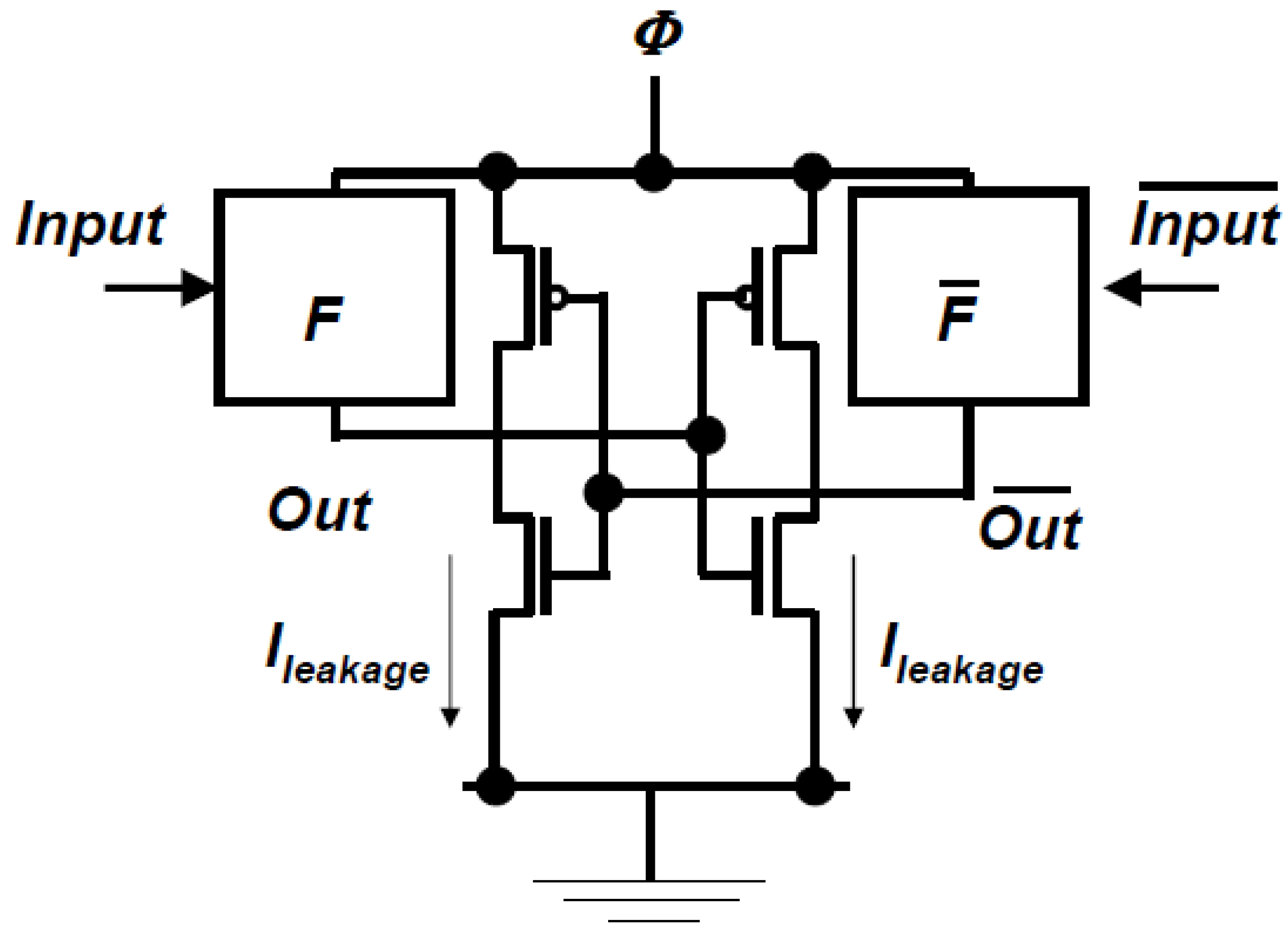
Figure 1.
Schematic representation of an equivalent logic circuit showing the four phase power clock with equal length segments: F represents the block logic function; RS is the series resistance dominated by the switch resistance; CL represents the load capacitance that is mainly due to interconnect capacitance; and CS represents the nanoelectromechanical switches (NEMS) variable capacitance. The current provided by the power clock is labeled i; the current going into the static interconnect capacitance (CL) is labeled i1; and that going into the variable capacitance of the NEMS switch (CS) is labeled i2.
4. NEMS-Based Adiabatic Logic Circuits
Nanomechanical switches are devices that rely on a beam, cantilever, or a membrane to deform under the effect of electrostatic force in order to make and break electrical contact upon the application of an external voltage. NEMS switching elements offer the property of zero leakage current [
5]. Although NEMS switches of varying design, dimensions and materials have been constructed and demonstrated, this paper relies on a 1-dimensional model as introduced in [
11] that may be applied to all devices equally in order to obtain a generic formulation of NEMS-based adiabatic logic circuits.
A typical 1-dimensional reduced order model of a 3-terminal electrostatic NEMS switch, where the structure is modeled by a simple parallel plate capacitor, is schematically represented in
Figure 4a: an electrostatic force is created between the gate electrode (G) and the suspended structure. When a bias voltage is applied, this force brings the structure which is connected to the drain (D), into contact with the source electrode (S). The source electrode is assumed to play no role in the electrostatic actuation of the structure. If the ratio of air gap
d to actuation gap
g is
![Jlpea 03 00368 i024]()
, an instability known as pull-in takes place. The pull-in results in a hysteretic effect as shown for an ideal
I-
V response plotted in
Figure 4b, in which case the voltage at which pull-in takes place, known as the pull-in voltage (
Vpi), is larger than the voltage at which the structure breaks contact, known as the pull-out voltage
Vpo. In case the contact is established before the onset of pull-in,
i.e.,
![Jlpea 03 00368 i025]()
, then there is only a contact voltage
Vcontact =
Vpi =
Vpo.
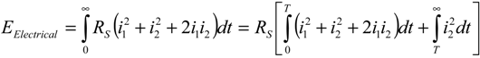
The total energy dissipation
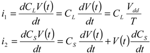
ETotal in a NEMS-based adiabatic circuit may be expressed as:
where
EElectrical and
EMechanical are the energy dissipated by the electrical resistance and the energy dissipated through mechanical damping respectively. While the mechanical energy dissipation may depend on the ramp period
T, it will be considered as a constant second order residue throughout this work.
Based on the equivalent circuit in
Figure 1, the electrical dissipation
EElectrical may be expressed as:
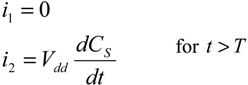
where
i,
i1 and
i2 are the currents going through the series resistance
RS, the load capacitance
CL and NEMS capacitance
CS respectively, as shown in
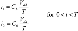
Figure 1. An expression for the current in each branch may be derived as follows:
From Equations (9) and (10), one can remark that the NEMS parameters governing the dissipation in an adiabatic circuit are the series resistance
RS and the time-dependent capacitance value of the NEMS switch
![Jlpea 03 00368 i026]()
. Furthermore, the minimum values of
Vdd and
T are set by the switch and therefore also dependent on the NEMS device.
Figure 4.
Schematic illustration of a reduced order model of a nanoelectromechanical switch (a) showing the source (S), drain (D) and gate (G). Also visible are the actuation and contact gaps, g and d respectively; V and I represent the actuation voltage and the source-to-drain current respectively; and ϕ represents the power clock signal; (b) Typical I-V plots in a NEMS switch operating in the pull-in mode, where Isat represents the saturation current of the device.
Therefore in order to obtain a comprehensive description of dissipation in NEMS-based adiabatic logic circuits, it is necessary to inject values for the switch series resistance and its transient behavior into Equations (9) and (10). These values are obtained from realistic contact mechanics models and dynamics NEMS models respectively, and are explicitly detailed below.
4.1. Contact Resistance in Nanomechanical Switches
The series resistance of an electromechanical switch is in fact dominated by the resistance at the contact between the movable and fixed electrodes [
12]. Therefore, proper electromechanical modeling of the contact resistance is crucial when designing NEMS relays based circuits.
Recent literature review of electromechanical contact in nano- and microelectromechanical systems [
13] indicate that to appropriately model the electromechanical contact, a multi-physics model that accounts for surface topography, elastic and plastic deformations, adhesion forces, surface contamination, and electron transport regime through the contacting areas needs to be employed. However, such complete modeling of contact aspects is beyond the scope of this paper, therefore a simplified contact model that considers two spherical asperities brought together under an applied force
Fapplied will be used.
Several models exist to describe the resulting interplay between the mechanical deformation of the asperities and the electrical behavior of the contact. Here, two common contact mechanics models will be considered, the Hertz contact theory [
14] and the JKR contact model [
15]. In addition, two electrical resistance models will be considered, the Maxwell resistance, and the Sharvin ballistic resistance.
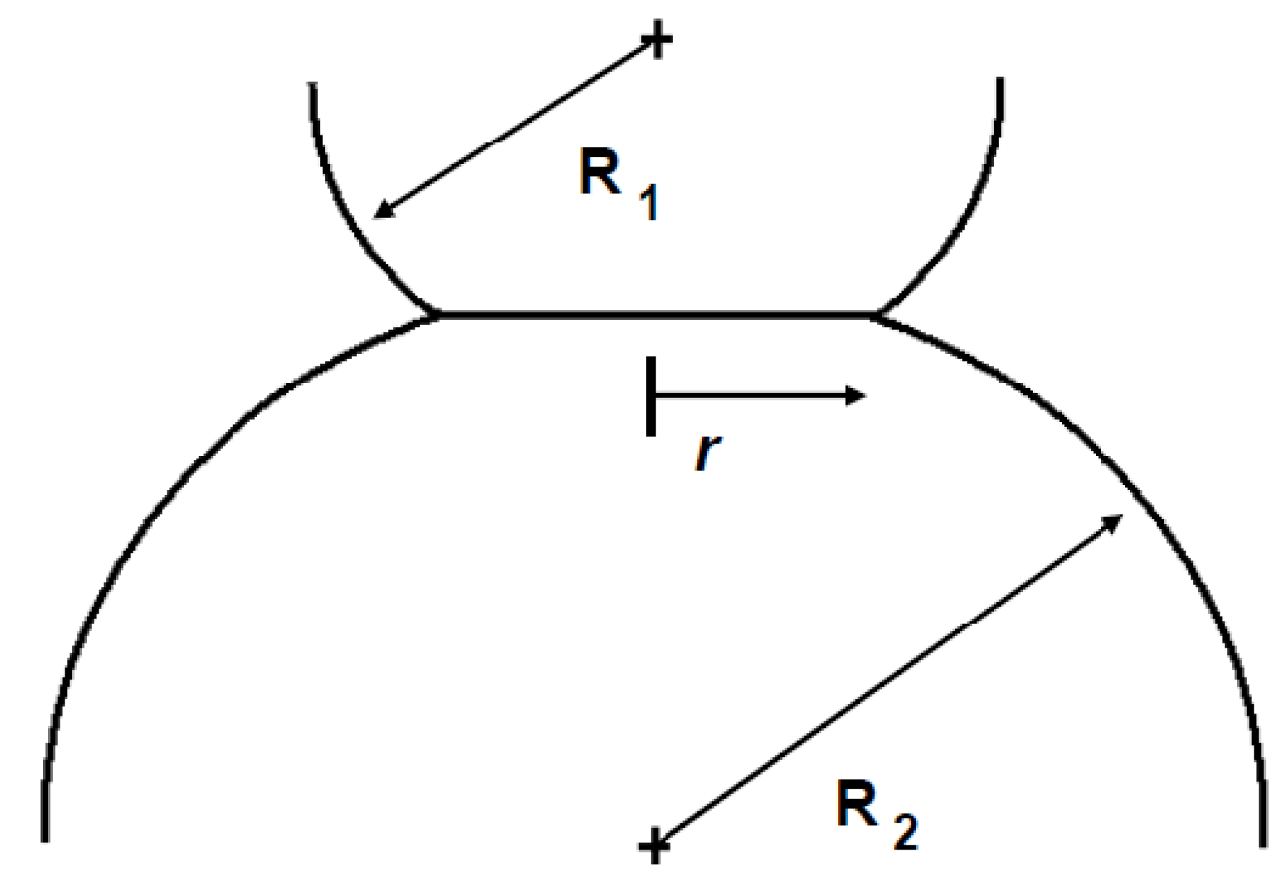
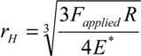
The Hertz contact assumes perfectly elastic deformations of two asperities, while at the same time neglecting any adhesion forces that may exist at the interface between the asperities: the radius
rH of the circular contact spot between two asperities shown schematically in
Figure 5, is given by:
where
R is the equivalent asperity radius given by
R = R1R2/(
R1 +
R2) where
R1 and
R2 are the radii of the first and second asperities respectively; and
E* is the effective elastic modulus given by
![Jlpea 03 00368 i028]()
, where
E1, ν
1,
E2, ν
2, are the Young moduli and Poisson ratios of the first and second asperities respectively.
In a reduced order model approximation, the force
Fapplied applied to the contacting asperities may be expressed as:
where
F0 is the minimum electrostatic contact force when
Vdd =
Vpi, and α represents the restoring elastic force; the exact values of both
F0 and α depend on the device design and fabrication. Note that Equation (12) only applies once contact is established,
i.e.,
Vdd ≥
Vcontact, regardless of whether the switch is operating in the pull-in or non-pull-in regimes.
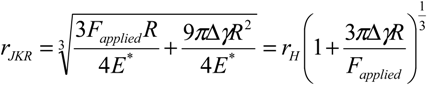
The Johnson-Kendall-Roberts (JKR) contact model on the other hand accounts for possible adhesion forces while also considering a purely elastic contact. A first order approximation of the contact radius in the JKR model is given by:
where
rJKR is the contact radius for a JKR type contact,
R and
K take the same values as expressed previously, and
Δγ is the net adhesion energy between the two surfaces.
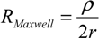
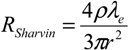
The electrical contact resistance given by Maxwell (
RMaxwell) in the diffusive transport regime, and Sharvin (
RSharvin) in the ballistic transport regime are respectively expressed as:
where
ρ is the electrical resistivity of the contacting asperities;
r is the contact radius as defined above; and
λe is the electron mean free path.
The expressions of the contact deformation and the contact resistance given by Equations (11) through (14), when combined together, give four electro-mechanical contact models. These contact models can be injected into Equation (9) to determine the effects of contact resistance on the total energy dissipation. The impact of these four models on the dissipation and performance of NEMS-based adiabatic logic circuits will be explored in the results and discussion section.
Figure 5.
Schematic illustration of two asperities in contact, deformed under the effect of an applied load.
Figure 5.
Schematic illustration of two asperities in contact, deformed under the effect of an applied load.
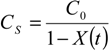
4.2. Switching Behavior of Nanomechanical Switches
The switching behavior of nanoelectromechanical switches will take on an important role in determining the losses in a NEMS-based circuit: this is due to the fact that the device capacitance,
i.e.,
CS, is inversely proportional to the time-dependent position
X(
t) of the movable mass, as given by the parallel plate capacitor value:
where we define
C0 as the NEMS switch capacitance in the initial position,
i.e., for
X = 0.
The question of the time dependent response of a NEMS switch has been treated to some length in literature for the case of step voltage actuation, which is the type of actuation envisioned for classical circuits; see for example [
6,
16]. Furthermore, the dissipation resulting from the transient current that is generated upon commutation under a step voltage actuation was also obtained [
17].
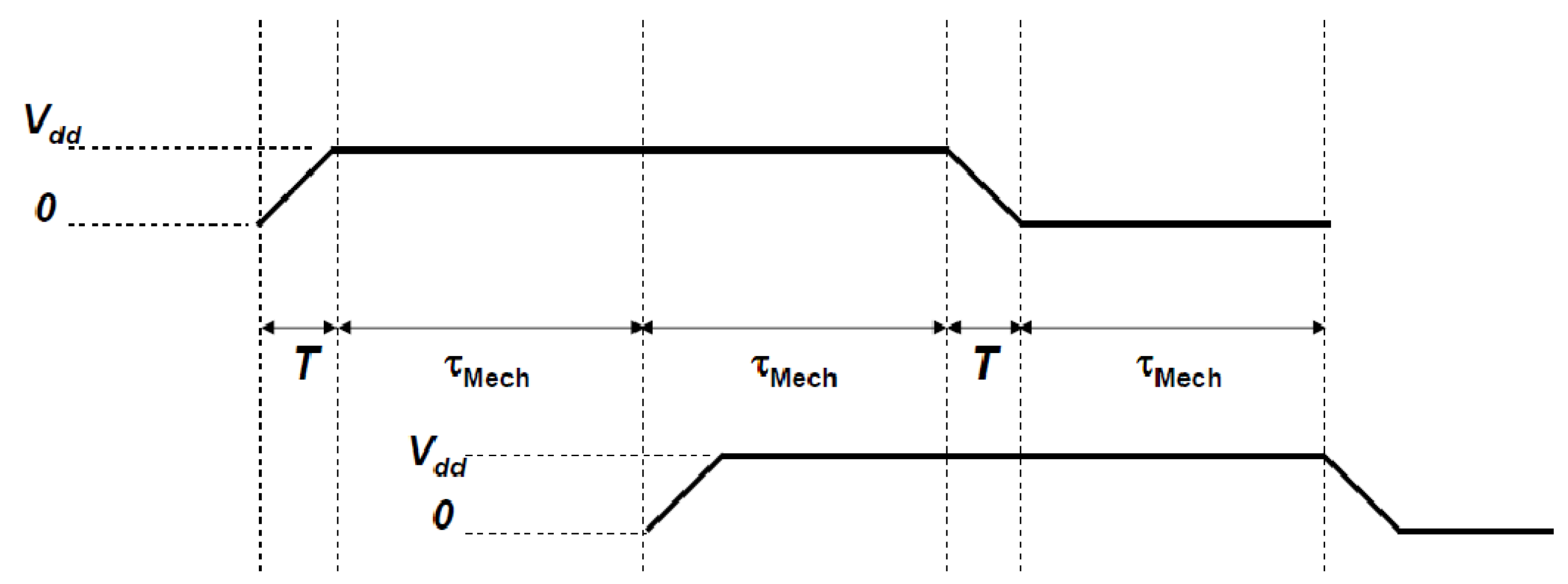
However, the voltage waveform in an adiabatic logic circuit is, by definition, required to be slowly varying. This constitutes the biggest difference between classical and adiabatic circuits with respect to NEMS dynamics. This fact results in an interplay between electrical and mechanical time constants, where the mechanical time constant is defined as the switching delay of the NEMS device. Therefore, two limiting cases will be considered separately, depending on the relations between the mechanical time constant (τMech), the electrical time constant (τElec), and the rise time of the clock signal (T).
First case (
τMech >>
T >>
τElec): in this scenario, that we will also refer to as “
dynamic mode”, the electric time constant is considered to be several orders of magnitude smaller than the mechanical time constant. The rise time of the clock signal is also much smaller than the mechanical time constant, such that from a mechanical point of view, the voltage would be ramped up to its hold value of
Vdd, before the mechanical structure even begins to move. Therefore, the structure responds in a manner that is similar to that when subjected to a step voltage. The net effect of this form of operation is to have a hold time that is significantly longer than the rise time, as shown in
Figure 6.
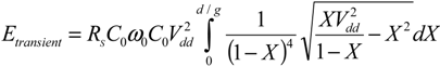
The electrical dissipation, in this case, may be obtained by decoupling the electrical and mechanical time scales by rewriting Equation (9) as follows:
The first term on the right hand side of (16) represents the dissipation due to the ramped electric charging of the interconnect and the switch capacitance: because the charging takes place during a time
T which is small compared to the
τMech, the switch capacitance is assumed to be a time-independent constant equal to
C0. While the second term represents the effect of a varying switch capacitance, which takes place upon mechanical commutation, under the effect of the now stable bias voltage
Vdd. For each of these terms, the currents are defined differently, given by:
The transient current in Equation (17b) and the resulting dissipation were derived explicitly in [
17], while the values in (17a) may be placed directly into Equation (16) to obtain a value for the electrical dissipation per switching operation. Furthermore, for the case of a switch response to an applied step voltage, the mechanically dissipated energy may be obtained by integrating the electrostatic force over the trajectory of the parallel plate [
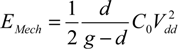
7], resulting in:
![Jlpea 03 00368 i027]()
, where
g and
d are the values of the actuation and contact gaps, respectively, as shown in
Figure 4.
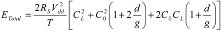
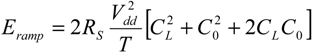
By combining Equations (16) and (17b), and including the mechanical losses, the total energy dissipated per switching cycle may be expressed as:
where:
and:
where all symbols in Equation (18a–c) take their previously defined meaning, and
ω0 is the mechanical resonance frequency of the spring-mass system that models the NEMS switch. The
ramp subscript is meant to represent the dissipation during the ramp-up and ramp-down phases of the power clock cycle.
Figure 6.
Schematic representation of the necessary clock signal for NEMS-adiabatic circuits working in the limit of (τMech >> T >> τElec ) with the hold phase lasting longer than the ramp-up and ramp-down phases. Also shown in the figure is the required synchronization between two phase clocks.
Figure 6.
Schematic representation of the necessary clock signal for NEMS-adiabatic circuits working in the limit of (τMech >> T >> τElec ) with the hold phase lasting longer than the ramp-up and ramp-down phases. Also shown in the figure is the required synchronization between two phase clocks.
Second case (T >> τMech >> τElec): another limit case to consider is when the rise time of the clock signal is slow compared to the mechanical time constant: therefore, the mechanical structure is assumed to move slowly. We will refer to this case as the “quasi-static mode”. Both the power clock rise time and the mechanical time constant are considered to be significantly longer than the electrical time constant.
It is important to note that, for this case, if the contact is to be established beyond pull-in, then a transient dissipation term will have to be introduced again into the dissipation equations, therefore negating the advantages that are sought to be obtained under this mode of operation. Therefore, for this case, only switches operating before pull-in will be considered.
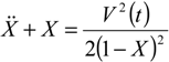
To obtain the response of a NEMS switch, and hence the dissipation, it is necessary to solve the following governing normalized nonlinear differential equation [
18]:
where
![Jlpea 03 00368 i029]()
, and
V(
t) is the time dependent ramp-up voltage; and
X(
t) is the time dependent displacement as shown in
Figure 4.
Equation (19) can only be solved numerically, and it is therefore difficult to provide a general solution for different values of ramp-up periods.
An approximate solution is therefore derived based on the hypothesis that the nanomechanical structure is moving slowly compared to its mechanical time constant (which is the underlying assumption for this case). More precisely, if
T >>
Q/ω0, where
Q is the mechanical quality factor, a solution based on static equilibrium equations is considered to be a good approximation. Such a solution is explicitly derived in [
19], and gives an expression for the total energy dissipation as:
In fact, two additional dissipation terms exist, one related to the mechanical dissipation, while the other is a non-adiabatic residue due to broken ramp-up ramp-down symmetry caused by adhesion forces. However, both these terms are small and are neglected in this analysis, as their derivation is beyond the scope of this publication.
5. Results and Discussion
From what is already introduced in the previous section, it is clear that the two most influential features of NEMS-based adiabatic circuits are: the contact resistance and the dynamic response of the switch.
The dynamic response of the switch and the way it affects power consumption are related to the mode of actuation of the switch, where a quasi-static actuation, i.e., “mechanically adiabatic”, is theoretically possible if a long enough ramp-up time is used. This form of operation of NEMS-switches is however less poised to be a candidate for practical adiabatic circuits, due to the low commutation speeds required for that mode of operation. In the dynamic operation mode, on the other hand, the switch is operated near its mechanical switching frequency, and consequently the adiabatic circuit operates near the NEMS switch commutation frequency.
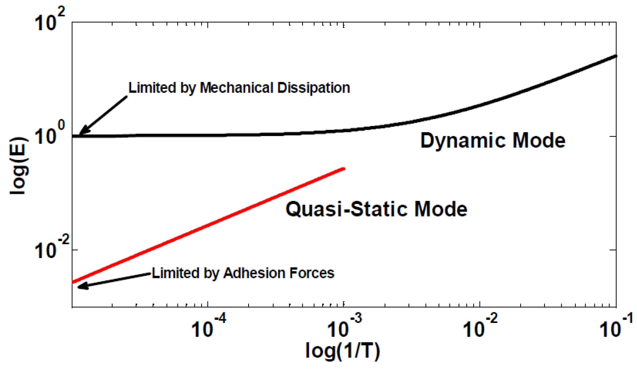
The difference between the two operation modes in terms of power dissipation as a function of frequency is plotted in
Figure 7; the energy is normalized with respect to
C0Vdd². The energy dissipation curves are calculated for
CL = 10
C0, a value chosen by industry standards [
20]. Additionally, the contact gap to electrostatic gap ratio is taken to be
d/g = 2/3. The horizontal axis of the graph in
Figure 7 represents the operating frequency of the circuit normalized to the nominal resonance frequency of the NEMS structure.
Figure 7.
Comparison of the performance of NEMS-based adiabatic circuits shown for: the dynamic mode of operation (black line) as given by Equation (18a–c), and the quasi-static mode of operation (red line) as given by Equation (20), both done for d/g = 2/3, and CL = 10C0.
Figure 7.
Comparison of the performance of NEMS-based adiabatic circuits shown for: the dynamic mode of operation (black line) as given by Equation (18a–c), and the quasi-static mode of operation (red line) as given by Equation (20), both done for d/g = 2/3, and CL = 10C0.
The first difference between the two operating modes shown in
Figure 7 is the frequency of operation, which differs by almost two orders of magnitude. The second difference is the magnitude of dissipated energy per operation. A difference of approximately two orders of magnitudes lower is observed for quasi-static operation. This latter effect is due to the mechanical energy dissipated per charge-discharge in the dynamic mode; this energy remains constant independently from the circuit operating frequency. Finally it is worth mentioning that, in the case of the quasi-static mode, adhesion forces set the lower limit of dissipation. Indeed, according to Equation (20) the energy dissipation limit is directly proportional to the contact resistance. As mentioned before, the JKR contact model considers the adhesion energy or adhesion force between the contacting asperties. Equation (13) indicates that the more the adhesion force, the larger the contact spot radius, and as a consequence the lower the contact resistance, whatever the electronic transport regime. The energy dissipation limit is then strongly influenced by adhesion forces. However the exact determination of adhesion forces requires significant efforts and is beyond the scope of this paper.
The contact resistance is a critical feature of a NEMS switch as it dictates energy dissipation and plays a direct role as it sets the RC/T adiabatic gain factor of the circuit.
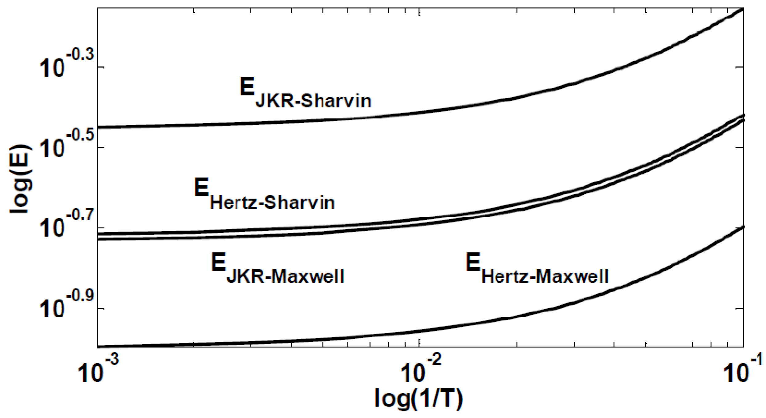
The energy dissipation of a NEMS-based adiabatic circuit operating in the dynamic mode is calculated and plotted in
Figure 8 for the different contact resistance models presented in
Section 4.1. These plots are based on a gold-gold contact with the following physical parameters: equivalent asperity
R = 4 µm, surface energy
Δγ = 1.4 J/m
2 [
15], electrical resistivity and electron mean free path of gold are
ρ = 22 × 10
−9 Ω·m, and
λe = 38 nm respectively.
Even though these classical contact models are used to simulate micrometer scale contacts, recent literature considers them to be inadequate to address nanometer scale contact, and expects the actual contact resistance to be more sophisticated to simulate and to present larger values than those actually given by the above models [
8]. In addition, these models are more suited to describe metal-metal contact, and give poor results when applied to semiconductor-semiconductor contact, as these latter ones may be dominated by tunneling currents [
8].
Therefore, contact resistance in nanomechanical relays remains a key parameter that dictates the adiabatic energy saving term in adiabatic logic circuits, and a parameter that needs further theoretical and experimental investigation.
Figure 8.
Plots of the contact resistance, described by Equations (11–14b), given by the different models on the performance of NEMS-based adiabatic circuits operating in the dynamic mode. The quasi-static mode is similarly affected (not shown) by the value of contact resistance values.
Figure 8.
Plots of the contact resistance, described by Equations (11–14b), given by the different models on the performance of NEMS-based adiabatic circuits operating in the dynamic mode. The quasi-static mode is similarly affected (not shown) by the value of contact resistance values.
At this point it is worth mentioning that having a supply voltage that is higher than the pull-in voltage, i.e., Vdd > Vpull-in, does not interfere with the proper operation of the circuit provided that the different phases of the power clock are well synchronized, and that is the case for both “dynamic mode” and “quasi-static mode”. This is because if the second power clock phase does not commence until the first one has started its hold value, the switch will already be in the close or open position (depending on the state) regardless of the supply voltage (as long as that is at least equal to the pull-in voltage) which is the purpose in exploring these limit case scenarios.
In fact a certain amount of voltage overdrive should be expected in any nanoelectromechanical integrated circuit, since fabrication variability will undoubtedly results in dispersion of the value of pull-in voltage. Therefore, in any NEMS-based logic circuit certain devices will be slightly overdriven, as it is the case with CMOS logic circuits. While this voltage overdrive does not interfere with the circuit function, it does result in an increased energy dissipation as given by equations (18a–c) and (20) depending on the mode of operation of the circuit.
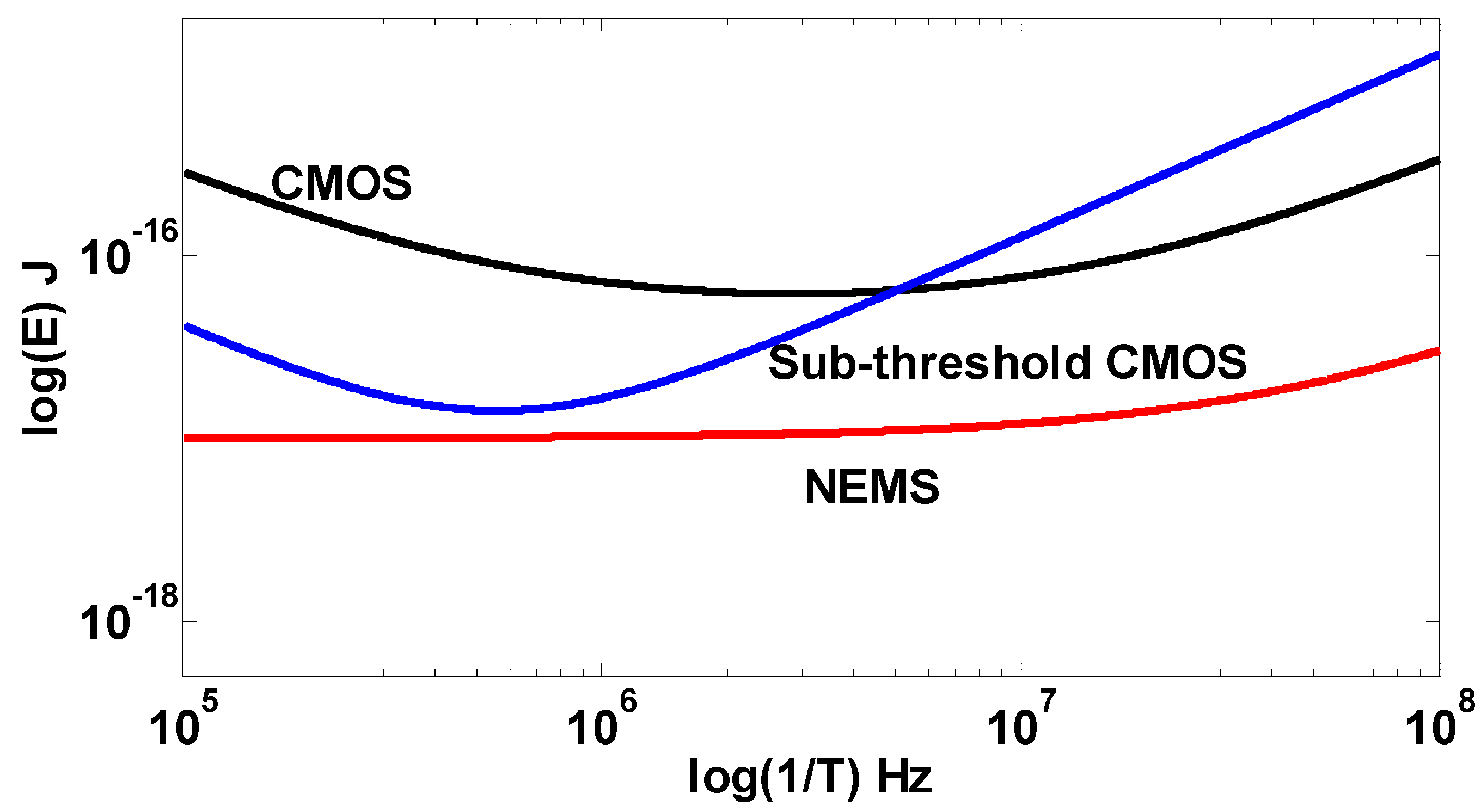
Finally, we would like to provide a numerical example that compares directly the expected performance of CMOS-based and NEMS-based adiabatic (operating in the “dynamic mode”) logic circuits. In this example we compare the performance of 45 nm CMOS adiabatic circuit with a 1 fF load capacitance to that of a NEMS switch with the following properties: device capacitance = 0.1 fF, pull-in voltage = 1 V, switching time > 1 ns, feature size = 50 nm, contact resistance = 10 KΩ, and a load capacitance of 1 fF.
The NEMS device parameters listed above correspond to the best projected parameters as expected by the ITRS roadmap [
20], as well as some parameters extracted from literature. Although a reliable NEMS switch with the above parameters have yet to be demonstrated, the following example gives an insight into the energy gain possible if the ITRS device targets are achieved. The results of this simulation are shown in
Figure 9, where the NEMS switch based circuit performs visibly more favorably than both classical and sub-threshold CMOS circuits.
Figure 9.
Plots comparing the performance of the classical (black) and sub-threshold (blue) CMOS adiabatic logic circuits (for 45 nm technology node and a 1fF load capacitance), and the performance of a NEMS-based adiabatic logic circuit (also with a 1fF load capacitance).
Figure 9.
Plots comparing the performance of the classical (black) and sub-threshold (blue) CMOS adiabatic logic circuits (for 45 nm technology node and a 1fF load capacitance), and the performance of a NEMS-based adiabatic logic circuit (also with a 1fF load capacitance).
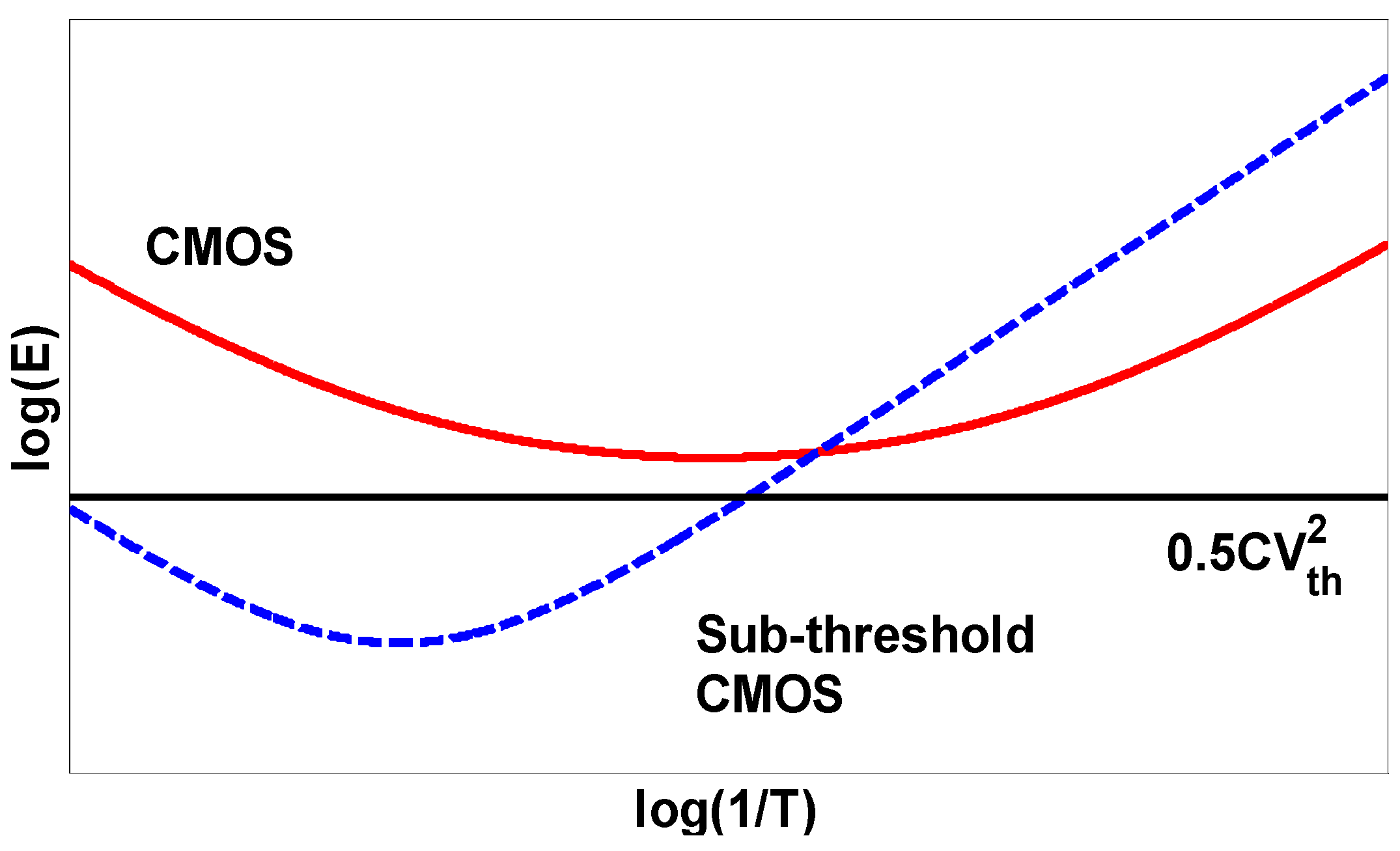
6. Conclusions
In summary, in this work, analytical expressions based on simplified circuit models were derived to obtain the performance limits of adiabatic circuits based on conventional CMOS, sub-threshold CMOS and NEMS based devices. Comparisons show that CMOS implementations are plagued by their leakage currents: when operating under a given frequency, the energy dissipation starts increasing again, and this remains the case for CMOS circuits designed and operated in the sub-threshold regime. It should be noted that the energy-optimum of sub-threshold CMOS is lower than that of a classical CMOS, but at high frequencies energy dissipation strongly increases.
It is also shown that for NEMS-based adiabatic circuits, an entire spectrum of possible operating regimes is available, from which two limiting cases were considered. In the first mode, the mechanical structure is assumed to be actuated similarly to a classical, i.e., non-adiabatic, NEMS-based circuit; while on the other operating extreme, the mechanical switch is assumed to operate slowly, in a quasi-static mode. These two operating modes offer contrasting performance in which either the circuit operating frequency is maximized at the cost of higher dissipation (dynamic mode), or the circuit energy dissipation is minimized at the cost of a lower operating frequency (quasi-static mode).
Furthermore, this paper identified several critical nanomechanical parameters that affect circuit behavior. In particular, the mechanical energy injected into the system limits the performance of NEMS switches operating in the dynamic mode, while adhesion energy will play a limiting role on the performance of quasi-statically operated switches. In both cases, it was also observed that the contact resistance of the NEMS device sets the magnitude of the dissipated energy; the full impact of contact resistance should be subject to further investigation, especially as it is correlated with adhesion forces.
Finally, it is of interest to note that the energy dissipated by NEMS-based adiabatic circuits is expected to be significantly lower than is the case of CMOS-based circuit, especially if low to medium circuit operating frequency is desired, a frequency range where their CMOS counterpart performs poorly due to static power loss.

 for a charge-discharge cycle. This remains the case regardless of the values of the series resistance or load capacitance.
 .
.

 ; and VDS is the source-drain voltage which is assumed to perfectly follow the power clock.
 , an instability known as pull-in takes place. The pull-in results in a hysteretic effect as shown for an ideal I-V response plotted in Figure 4b, in which case the voltage at which pull-in takes place, known as the pull-in voltage (Vpi), is larger than the voltage at which the structure breaks contact, known as the pull-out voltage Vpo. In case the contact is established before the onset of pull-in, i.e.,
  , then there is only a contact voltage Vcontact = Vpi = Vpo.
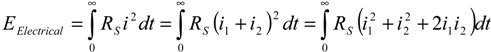
 . Furthermore, the minimum values of Vdd and T are set by the switch and therefore also dependent on the NEMS device.
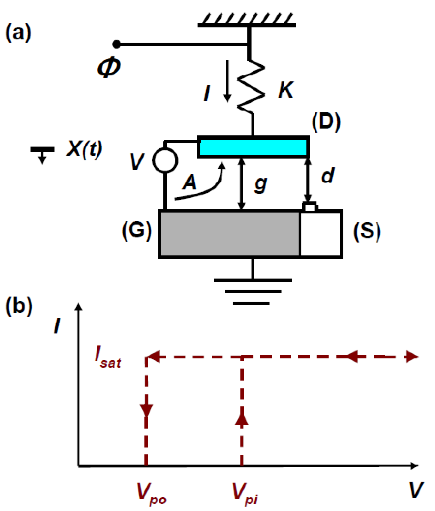
 , where E1, ν1, E2, ν2, are the Young moduli and Poisson ratios of the first and second asperities respectively.
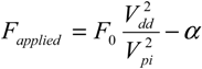

 , where g and d are the values of the actuation and contact gaps, respectively, as shown in Figure 4.

 , and V(t) is the time dependent ramp-up voltage; and X(t) is the time dependent displacement as shown in Figure 4.