1. Introduction
As integrated circuit feature size continues to shrink and wireless and portable devices grow, power consumption not only becomes one of the key issues to be considered during functional operation, but also has to be addressed during manufacturing tests. High power consumption during the functional operation implies:
Higher design and manufacturing costs due to the extra effort to calibrate power grids in order to meet the power supply requirement.
Higher system costs due to packaging and cooling requirements.
Shorter device life cycle and lower device reliability.
Shorter battery life for portable devices.
In order to reduce the functional power consumption, various low power management techniques have to be implemented during design phase [
1–
5]:
Power domain: The device is implemented by including multiple functional blocks. Each functional block can be independently powered up or down by controlling the power switches used to gate the power supply connection to each functional block.
Multiple supply voltages: Depending on operation conditions, a power domain can be operated under different supply voltages. The power domains operated at different supply voltage levels are connected through level shifters.
Isolation logic: The logic locates at the boundary of two power domains in order to isolate the power-off domain from the power-on domain.
State retention cell: A special sequential state element that preserves its state when the power domain containing this sequential state element is powered down.
Power mode: A functional operation mode that makes each power domain operate at either the power-on or power-off state and assigns specific supply voltages to each power-on domain.
Clock gating: A powerful technique to reduce the power consumption in a power-on domain through dynamically blocking the clock pulse to reach a set of sequential state elements. The clock gating is often hierarchically implemented in order to improve the flexibility to control the power consumption during functional operation.
In order to meet the design methodology changes in the low power designs, traditional design-for-test (DFT) methodologies have to become power-aware such that:
The power constraints should not be violated by the test programs and the DFT architecture included into the design.
Power management circuitry, including isolation logic, state retention cells, level shifters, and power switches, etc., have to be tested adequately.
ATPG should effectively utilize the embedded clock gating logic to reduce the test power.
DFT hardware added to generate the low power test patterns and to improve the testability of the low power management circuitry should minimize its area overhead and avoid its impact on system performance while maximizing the benefits to reduce the test power and the test cost.
Test scheduling plans should cover all power domains, glue logic, and all supply voltage levels while minimizing test application time and test data volume and reducing overall test power consumption.
Besides taking functional power management into account, it is also necessary to make the test power consumption close to the worst-case functional power consumption in order to avoid yield loss, reliability degradation, and permanent damage of a circuit. It has been shown that scan based tests significantly reduce the test cost and achieve satisfying test quality as compared to functional tests. However, it was also observed that the scan based tests may cause circuit switching activity in excess of the activity during normal operation. The main reason is that the scan test patterns often make the circuit operate in non-functional states. On the other hand, as the small delay defects become one of dominant defect types introduced during manufacture due to the process variation, at-speed test set based on transition fault model become mandatory to be included in the test suites in order to achieve adequate test quality. It has been shown that IR drop issues caused by the excessive test power consumption reduce the effectiveness of at-speed scan testing, resulting test escape due to clock stretch [
6], and yield loss due to incorrect capture caused by additional gate delay [
7]. Test power reduction in the scan based tests has become more urgent in today's nanometer designs.
In the scan based tests, there are two types of test power: average test power and peak test power. The former is the ratio of consumed energy over a time period to the test time, while the latter is the highest power value at any given instance [
8].
Excessive average test power consumption may cause the problems listed below [
8]:
The increased thermal load on the circuit under test is likely to create hot spots that damage the silicon, the bonding wires, or even the package.
Elevated temperature and current density in test mode will increase electro-migration, which in turn causes more intensive erosion of conductors that severely decrease the reliability of the device.
It is imperative to use expensive package to tolerate excessive heat during test.
When the peak power is beyond the design's limit, the circuit cannot be guaranteed to function correctly since the supply voltage droops introduce additional gate delay and may cause false failure.
The test power consumed during scan shift and during capture is referred to as shift power and capture power, respectively. The average power consumption is determined by the shift power. Excessive shift power accumulation may cause scan chain failure and can impact the test responses captured in the capture cycles. During capture, the power reduction is typically focused on the peak power since it may cause supply voltage droops resulting in yield loss and/or test escape due to the additional gate delays and/or the clock stretch.
Over the years, numerous techniques for test power reduction in shift and capture modes have been proposed, including test scheduling [
9], test vector reordering [
10], partitioning [
11], X-fills [
12–
14], blocking gate [
15–
19], and clock gating [
20–
23],
etc. In general, an ideal test power reduction strategy should include the following properties:
It makes the test power consumption close to functional mode.
It has low area overhead and no impact on functional operation.
It is easily integrated in design flow.
It can be used in the test compression environment.
It has no impact on test coverage and supports all fault models.
It has minimal impact on test data volume and test application time.
Obviously, it is hard to find the ideal test power reduction strategy. For example, methods to reduce capture power consumption often increase the test pattern count. As a result, a compromised decision has to be made during design phase in order to balance between the low power testing requirement and the additional test cost. In order to test the functional power management circuitry appropriately and choose appropriate DFT techniques to reduce the test power consumption, the power-aware testing capabilities provided by the commercial DFT tools should be understood thoroughly by the test engineers.
The objective of this paper is to provide a comprehensive overview of the power-aware testing capabilities provided by the commercial DFT tools. The following topics will be covered in this paper:
Section 2: Test power estimation.
Section 3: Testing of power management circuitry.
Section 4: Low power ATPG techniques to reduce the test power consumption during shift and during capture.
Section 5: Brief discussion about test scheduling for multiple power domains and its impact on test cost.
2. Test Power Estimation
To quantify the power dissipation consumed by test patterns, several test power estimation methods have been proposed to guide the test generation process. They can be classified into two categories:
Non-timing based approach: Non-timing based logic simulation is used in this approach. The switching activity occurred at a gate in a clock cycle is weighted based on the gate load. The sum of the weighed switching activity (WSA) among all the gates is used as the test power estimation for the clock cycle. Typically, the weight can be chosen as unit weight, the number of the gate's fanout plus 1, or load capacitance.
Timing based approach: During every clock cycle, timing based simulation is used to record specific time instance that the gate switches. The clock cycle is divided into multiple time slices and the WSA is calculated for each time slice. The time slice with the maximum WSA is used as the peak test power estimation in this clock cycle.
These two approaches can be enhanced further by taking the power grid network into account in order to estimate regional test power more accurately [
24].
When guiding ATPG to generate low power test patterns, it requires that the test power estimation approach not only has less impact on ATPG performance, but also provides sufficient accuracy. As a result, the non-timing based approach is often preferred. Typically, the commercial DFT tools are able to report the power consumed by each test pattern during scan shift and during capture.
During scan shift, the transitions occurring at each scan cell are weighted to estimate the shift power. The test stimulus in current test pattern and the test response captured from previous test pattern are considered simultaneously in order to report the shift power more accurately. For a scan chain
j including
C scan cells, its weighted transition is calculated as follows:
where
S is the number of shift cycles and
S ≥
C;
ri,
i ∈ {1…
C}, is the test response captured at scan cell
i after applying the previous test pattern;
ti,
i ∈ {1…
C}, is the test stimulus assigned to scan cell
i at the end of the shift operation; and
ti,
i ∈ {(
C + 1)…
S}, is the test stimulus shifting into the scan chain when the number of scan cells in the scan chain is less than the number of shift cycles. Moreover, thescan cell 1 in a scan chain is the cell driven by the scan input pin. The shift power is equal to the sum of the weighted transitions among all the scan chains.
During capture, the non-timing based logic simulation is carried out to determine the switching activity of each gate in each clock cycle. The weight being equal to the number of gate fanout plus 1 is typically used to calculate the WSA. For each test pattern, following capture power metrics are reported by the commercial DFT tools:
Peak WSA: The largest WSA among all the clock cycles.
Average WSA: The sum of WSA of all the clock cycles over the total number of clock cycles.
Peak of state transition: The largest number of transitions occurring at sequential state elements among all the clock cycles; unit weight is used.
Average of state transition: The sum of the transitions occurring at sequential state elements in every clock cycles over the total number of the clock cycles; unit weight is used.
For each capture power metric listed above, the commercial DFT tools are also able to report them based on instances in the design. If we assume that the logic gates within an instance are implemented in the same region within a die, the power metrics for the instances can be used to estimate the regional test power such that it provides an approximate way to find the hot spot caused by each test pattern.
Besides the reporting capability for the shift power and the capture power, the commercial DFT tools also provide a test pattern rejection mechanism that filters out the test patterns with power metrics violating the predefined thresholds and the test pattern ordering based on the test power consumption.
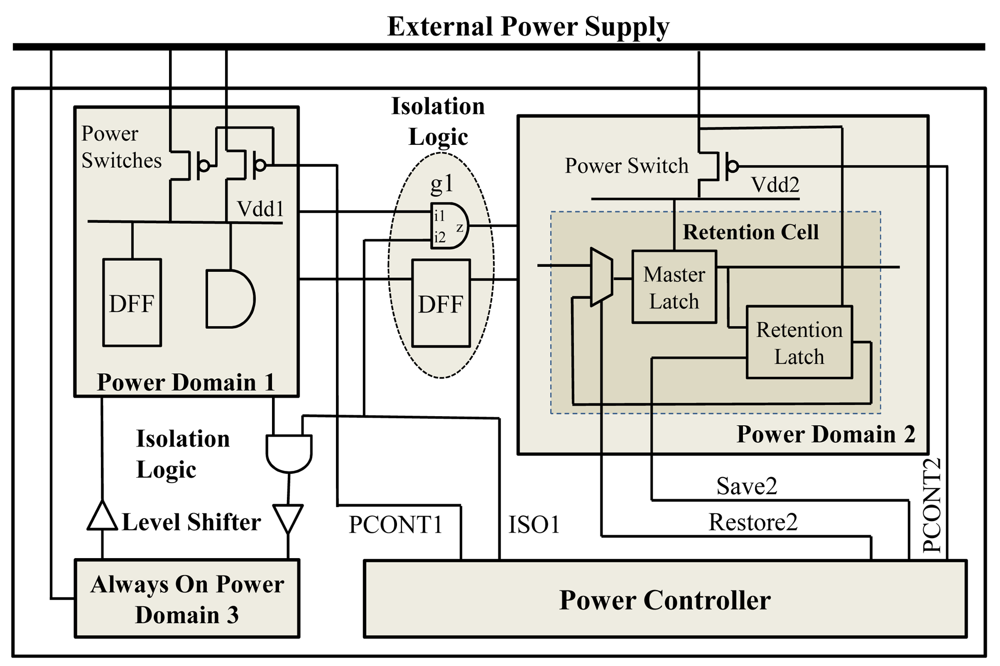
3. Testing of Power Management Circuitry
The key components in a typical power management circuitry are shown in
Figure 1. The structure and the operation of the power management circuitry can be described by either Unified Power Format (UPF), which is going to become IEEE standard as P1801, or Common Power Format (CPF), which was developed by Cadence. The main contents defined in the UPF/CPU include:
A list of power domains and the control method for their power switching logic.
A list of power modes and the operations and the supply voltages for each power domain under each power mode.
Logic connection among power domains through isolation logic and/or level shifters.
A list of retention cells included in each power domain and the method to save (restore) the state of the retention cells when the power domain is powered down (up).
Besides applying the traditional DFT rules to check the integrity of the design for DFT insertion and for ATPG based on scan, the commercial DFT tools have to include a set of new rules to take the functionalities of the power management circuitry into account in order to ensure the scan based tests are effective and applicable. Typically, the new rules check the following:
The power data loaded from UPF/CPF are correct and cover the operations of every power domain under every power mode.
The scan chain spanning multiple power domains cannot power down some of its scan cells and power up the rest simultaneously.
All control logic for the scan operation must be powered on during scan shift.
The power domains under test cannot be incorrectly powered down during capture.
All power control signals, including isolation signals, retention save/restore signals, and power switching control signals, etc., must be generated from always-on power domain(s).
Level shifters must be inserted at the paths connecting the power domains operated in different supply voltages.
Isolation cells must be inserted at the paths connecting the power domains that can be powered down independently.
To improve the testability for the power management circuitry, DFT structure, such as the Power Test Access Mechanism (PTAM) [
2], can be inserted in the design by using the DFT insertion tool. During test, this structure generates signals that override the control signals from the functional power controller. This improves the flexibility to schedule the testing order for power domains, ensures the power domains hold their power state in the middle of test, and ensures the isolation between power domains with different power state,
etc. In this section, we only provide a brief overview about how to generate tests for some components included in the power manager circuitry.
3.1. Power Switches
The power switches shown in
Figure 1 are used to control power state of a power domain. Testing the power switches can be performed either implicitly or directly. The implicit test is done when the power domain gets tested. For example, to test power switch stuck-open, one can use the test patterns for retention cells and detect the failures by observing the unloading value from the retention cells. When the power switches are implemented by using the daisy chain, as shown in the power domain 1 in
Figure 1, delay testing can be used to test part of the power switches stuck-open. This strategy does not require additional DFT hardware, but it has difficulty diagnosing the faulty switches implemented by using the daisy chain. The preferred method is to insert DFT control and observation points at the power switches in order to deterministically detect failures through comparison of the voltage at each power switch output with a reference voltage. One example of DFT implementations can be found in [
25]. However, this technique suffers from long discharge time that may either lead to false pass or long test time. In [
26], the extra discharge transistors are added to reduce the discharge time during test application.
Although the power switches are effective in reducing the static power by powering off the logic blocks in idle mode, it requires long wake-up time when reactivating the logic blocks from the idle mode. The intermediate strength power gating was proposed in [
27] to achieve the trade-off between suppression of leakage current and shorter wake-up time. To test this type of power-switching structures, a signature analysis technique was proposed in [
28]. The proposed DFT technique converts the voltage at virtual power rail or virtual ground rail into a frequency reading. The converted data is shifted out from the scan chain in order to detect and diagnose the failure power switches.
3.2. Isolation Cells
Testing the isolation logic located between two power domains completely will require:
For example, to test the isolation AND gate
g1 shown in
Figure 1, the functional power controller should be configured to the power mode that powers up the power domains 1 and 2 and to set the isolation enable signal
ISO1 to 1. Under this configuration, the test generator creates tests for the faults at
g1/i1 and
g1/z and the fault
g1/i2 s-a-0. To detect the fault
g1/i2 s-a-1, the functional power controller has to set
ISO1 to 0 and it requires a power mode that powers up the power domain 2 and powers down the power domain 1. Due to the unknown value at
g1/i1, the fault is untestable. To generate a test deterministically for this fault, the DFT structure such as PTAM is needed to enable the test generator to take control of
ISO1 when both the power domains are powered up.
3.3. Retention Cells
To test the retention cells included in a power domain, a power mode that powers up this power domain is selected first in order to ensure the scan shift operation can load and unload known value from the retention cells. During capture, a test sequence includes the following sub-sequences:
In commercial ATPG tools, the capture test sequence can be defined in the test procedure and the ATPG tool will automatically generate retention test patterns based on it to verify the capability of the retention cells retaining 0 and 1. In the commercial ATPG tool FastScan®, the capture test sequence for retention test is described by using named capture procedure that defines the complete clock sequence between scan loading and unloading.
3.4. Level Shifters
The level shifter is typically modeled as a buffer for test generation purposes. To generate tests for a level shifter located between two power domains, it requires a power mode that powers up both power domains. Moreover, if the power domain can operate in multiple supply voltages, the level shifter needs to be tested repeatedly under different supply voltages.
4. Low-Power ATPG Techniques
Although many ATPG techniques to reduce the test power have been proposed in the past, all of these techniques require additional test cost. When choosing the low power test techniques for a design, one has to consider the tradeoff among test application time, test data volume, area overhead, and performance impact, etc.
Typically, the low power ATPG techniques supported by the commercial tools are based on X-fill strategies, clock gating control, blocking scan cell outputs, and clock application schemes. These techniques can be used alone or together.
4.1. X-Fill Strategies
X-fill utilizes the unspecified bits in a test cube to reduce shift power, capture power, or do both simultaneously. The main advantage of using X-fill strategies is that they are a non-intrusive method, have no impact on system performance, and require no additional hardware if applying in non-test compression environment.
The motivation of using X-fill strategies comes from the observation that a test cube typically contains less than 1% of care bits. The unspecified bits in the test cube can be filled with any values without losing test coverage. However, comparing to fill the unspecified bits randomly, the low power X-fill typically generates more test patterns due to the lower probability of detecting faults by chance.
To reduce the shift power, 0-fill and 1-fill assign 0 and 1 to X bits, respectively, while adjacent fill assigns X-bits to be the same as the nearest care bit [
12].
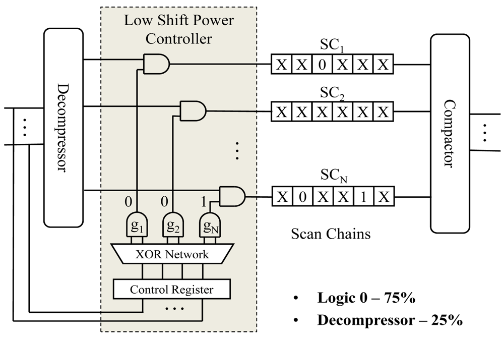
When performing test generation in the test compression environment, X-fill is less effective due to the limitation of encoding capacity enforced by the on-chip decompressor. Without additional DFT hardware, it is also inapplicable when the compression ratio is high. In [
29], the low shift power decompressor was proposed by inserting a low shift power controller between decompressor outputs and scan chain inputs. Based on the observation that the majority of scan chains have no specified bit in each generated test cube, this method fills a large percentage of scan chains with constant 0.
Figure 2 shows the low shift power controller that fills approximately 75% of scan chains with constant 0 during scan shift. The logic values assigned at the outputs of the gate
g1 to
gN are dynamically determined by the generated test cube. For example, the test cube shown in
Figure 2 specifies one scan cell with loading value other than 0 in the scan chain
SCN. Therefore, the low shift power controller generates 1 at the output of
gN such that
SCN is driven by the decompressor. In the scan chains
SC1 and
SC2, the scan cells have either unspecified value or loading value 0. Enforcing
g1 = 0 and
g2 = 0 makes the constant 0 shift into these two scan chains such that the shift power is reduced.
In order to support the adjacent fill, a shadow register can be inserted between the decompressor outputs and the scan chain inputs such that the test stimuli feeding the scan chains could be held for some shift cycles [
30] during scan shift.
When considering the capture power reduction, the X-fill techniques, such as LCP fill [
13] and preferred fill [
14], reduce the hamming distance of the logic values captured into the sequential state elements between adjacent clock cycles. The less the number of sequential state elements changes their state during capture, the lower the switching activity occurs in the combinational logic. Due to the limitation of the encoding capacity, it may be inapplicable to reduce the capture power based on these techniques in the test compression environment when the compression ratio is high. Fortunately, it has been observed that filling 0 for majority scan chains can reduce the capture power significantly. Therefore, the low shift power controller shown in
Figure 2 reduces the capture power as a byproduct and also helps to reduce the switching activity caused by the test responses when shifting them out from the scan chains.
4.2. Clock Gating Control
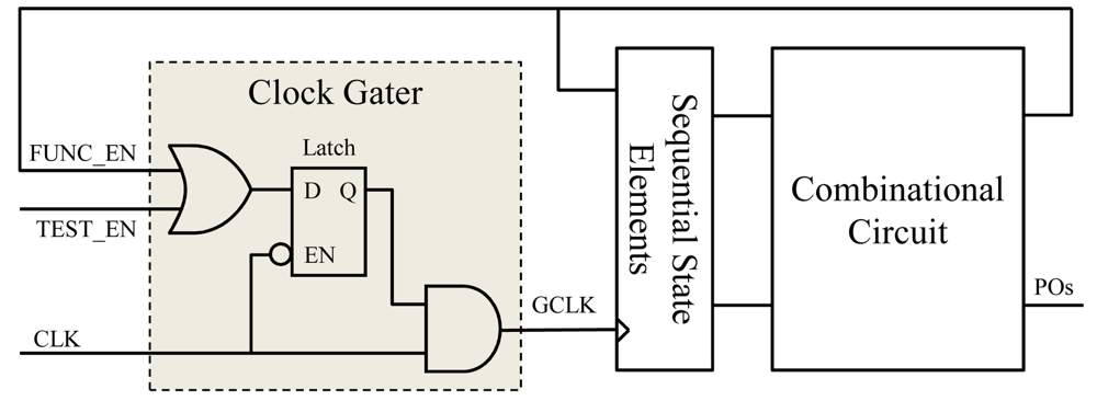
To control the power consumption in the power-on domains during functional operation, the low power designs often insert clock gaters in the clock paths during logic synthesis to dynamically block the clock pulse to reach sequential state elements. During test generation, the ATPG tool can utilize these existing clock gaters to reduce the capture power consumption.
Figure 3 shows a typical clock gater architecture embedded in a design. During shift,
TEST_EN is asserted in order to allow
CLK pass through the clock gater to shift the scan chains. During capture,
TEST_EN is deasserted and the clock gater is controlled by its functional enable pin
FUNC_EN. To reduce the capture power, the test generator can deassert the
FUNC_EN if the sequential state elements controlled by the clock gater are not used to activate, propagate, and/or observe targeted faults. In order to effectively control the clock gaters during test generation, the sequential state elements controlling
FUNC_EN should be scan cells.
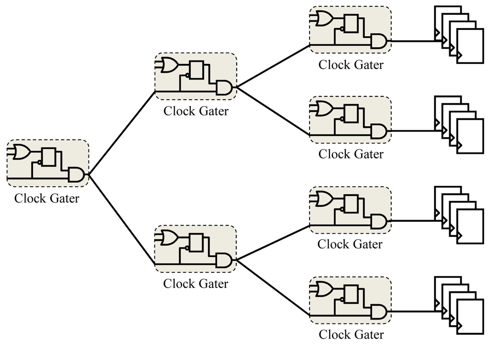
To maximize the flexibility of the power control during functional operation, clock gaters are often designed in a hierarchical way in order to achieve both fine and coarse levels of control granularity as shown in
Figure 4. This kind of architecture is preferred, especially when doing the test generation in a test compression environment. With the coarse control, fewer control bits are needed to prevent the clock pulse from reaching a large percentage of sequential state elements. As a result, less care bits need to be encoded by the decompressor. With the fine control, the test generator can utilize spare encoding capacity to reduce the capture power further. On the other hand, the control conditions for the clock gaters at low level are not always unique and/or mutually exclusive. It is possible that one condition deasserting a clock gater asserts another clock gater although the condition deasserting both clock gaters exists. Without a higher level clock gater that controls these two clock gaters simultaneously, it is hard for the test generator to always find the solution that deasserts both of them when they are not used to detect the targeted faults. The hierarchical clock gaters make the test generator more effective to generate test patterns with lower capture power.
The test generation procedures that utilize the clock gaters to reduce the capture power can be found in [
29] and [
31]. The main steps including those procedures are summarized as follows:
Automatically identifying the clock gating logic.
Before doing test generation, the preprocessing step generates a set of test cubes that deassert the FUNC_EN pins controlling one or more clock gaters.
During test generation, the test cube detecting the targeted faults is merged with the test cubes that disable as many clock gaters as possible.
Apart from reducing the capture power during test generation, the set of test cubes for controlling the clock gaters can also be used for the purposes listed below:
Providing a fast but approximate way to estimate the power consumption for a partially specified test cube such that the generated test cube detecting a set of target faults can meet predefined switching threshold.
Estimating the effectiveness of utilizing clock gaters to reduce the capture power; this is achieved by counting the percentage of the sequential state elements controlled by the clock gaters as well as the granularity of the number of the sequential state elements controlled by each test cube.
Estimating the impact on test compression by counting the number of care bits that are included in each clock gater control test cube.
Similar to the X-fill strategies, utilizing the clock gaters to reduce the capture power often results in higher test pattern count, but it can effectively reduce the test power consumption in both the data path and clock tree. This is the preferred strategy for the capture power reduction.
Clock gating can be used to reduce the shift power with additional DFT hardware. In [
21] and [
22], an independent clock control is associated with each scan chain that disables/enables the shift clock to drive the scan chains during scan shift. By shifting a portion of scan chains for each test pattern, the shift power consumed by both the clock tree and the combinational logic is reduced. The low shift power architecture shown in
Figure 2 is extended to gate the shift clock in [
23] such that a subset of the scan chains is enabled to be shifted in the test compression environment.
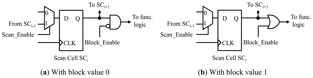
4.3. Blocking Scan Cell Outputs
Since the switching activity at the combinational logic in a design is caused by the state changes at the sequential state elements, the test power consumption in the data paths can be reduced by blocking the transitions occurred at the sequential state elements propagates to the combinational logic during shift or capture. Two implementations of gating the scan cell output to be 0 and 1 are shown in
Figure 5a,b, where an AND gate and an OR gate are added as the blocking gate, respectively. By asserting
Block_Enable signal, the transition occurred in the scan cells is blocked. During normal operation, this signal is de-asserted.
To reduce the shift power, the method in [
15] inserts the blocking gates at every scan cell outputs. In order to reduce the hardware overhead, a subset of scan cells, named power sensitive scan cells, is identified by [
16,
17] based on signal probability analysis and the blocking gates are inserted only at these scan cells in order to achieve the tradeoff between the shift power reduction and area overhead. Similar technique based on the random simulation for scan cell selection was proposed in [
18] as well, but it suffers from high computation complexity.
The method utilizing the blocking gates to reduce the capture power was proposed in [
19]. A set of special scan cells, named block enable cells, is inserted to the scan chains in order to dynamically control the blocking gates during capture. The extension of applying this method in the test compression environment was also addressed in [
19] by adding a capture power controller similar to the one shown in
Figure 2.
4.4. Clock Application Schemes
Since the dynamic power consumption is triggered by clock pulse, the clocking schemes can be manipulated to reduce the test power with or without additional DFT hardware.
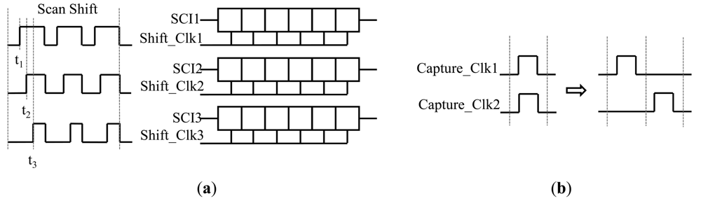
To reduce the shift power, the scan chains can be partitioned into multiple groups. Each group is either shifted at a different time within a clock cycle [
32] or shifted at the different clock cycles [
11].
Figure 6a shows the clock scheme to shift three scan chains at the different times,
t1,
t2 and
t3, in a shift cycle [
32].
When doing test pattern generation, the test generator prefers to pulse as many clocks belonging to the same clock domain simultaneously as possible during capture in order to minimize test pattern count. In order to reduce the capture power, the ATPG tool can restrict the number of clocks pulsed in the same capture cycle. To avoid the increase of test pattern count, those capture clocks belonging to the same clock domain are pulsed sequentially in different clock cycles as shown in
Figure 6b. Since the test application time is dominated by the scan shift, adding extra capture cycles have negligible impact on overall test application time.
5. Test Scheduling
To reduce design cost, most of modern SOC designs use modular structure. Each module may be designed and optimized by using its own low power test techniques. When testing the whole design, targeting one module at a time while keeping the remaining modules in a steady state can minimize the test power consumption. However, it increases the test cost due to the longer test application time. Testing multiple modules in parallel is an alternative solution to reduce the test cost. But it may cause violation of the power constraints when the low power management features in the designs are not considered. Therefore, the test scheduling algorithm has to add the test power as an additional dimension for optimization.
In the past, researchers had proposed a lot of test scheduling algorithms optimized for different goals. For example, the test data applied to the modules under test are transported from the top-level through a test access mechanism (TAM) shared among different modules. The test application time can be reduced by optimizing bandwidth supported by the TAM [
33]. However, fewer studies were published in the area of test scheduling for low power designs. The most recent research work to reduce the test cost by optimizing test scheduling for multicore SOCs with multiple supply voltages can be found in [
34].
Unfortunately, the power-aware test scheduling for the low power designs is still a grey area for the commercial DFT tools. The DFT tools can only provide some guidelines about the test scheduling to reduce the test cost and check the correctness of the test access mechanism from top-level to the modules under test as well as check the isolation of the modules under test from the surrounding logic during test application. It depends on test engineers to plan the test strategies for multiple modules by taking test cost and power constraints into account. This area needs to be covered by the commercial DFT tools in the near future.
6. Conclusions
In this paper, we present the capability of the commercial DFT tools to test the designs with power management circuitry and review the low power ATPG techniques supported by the DFT tools. The power metrics used and reported by the tools are also discussed. Although the commercial ATPG tools cannot cover all the existing low power test techniques due to development and maintenance efforts, they support most popular techniques that can meet majority requirements, especially utilization of these techniques in the test compression environment.
As the test challenges for low power designs continue to increase, the commercial DFT tools also need to be enhanced to follow the new requirements while ensuring the highest test quality and minimizing test cost. For example, rather than minimize the capture power as much as possible, the capture power during test should be close to the functional power in order to avoid under testing. Finally, supporting an automatic test scheduling for complex SOC is another main goal that needs to be addressed.
