Fabrication and Performance of MEMS-Based Pressure Sensor Packages Using Patterned Ultra-Thick Photoresists

Abstract
:1. Introduction
2. Packaging Design
2.1. Packaging Concept
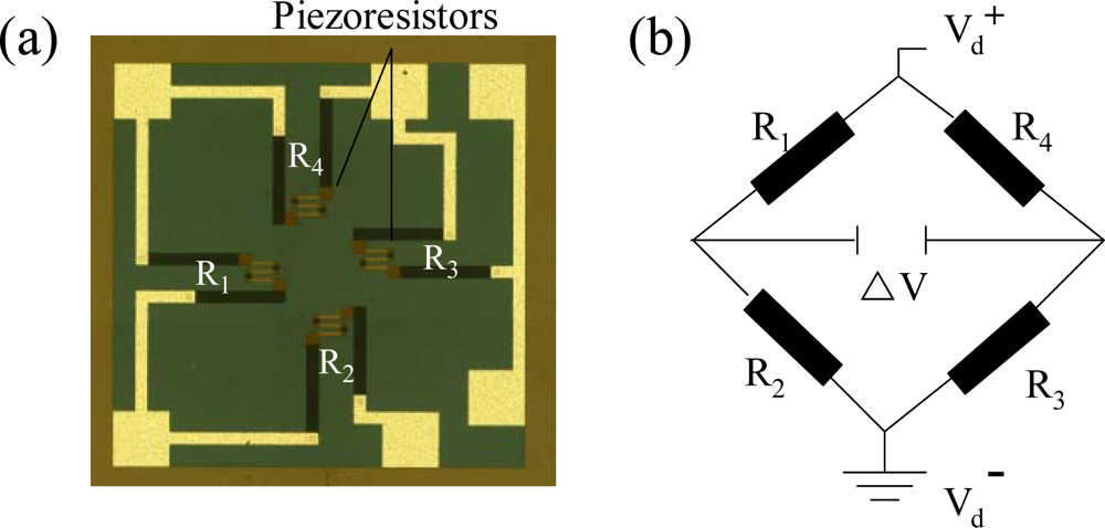
2.2. Piezoresisive Pressure Sensor
2.3. Packaging Process
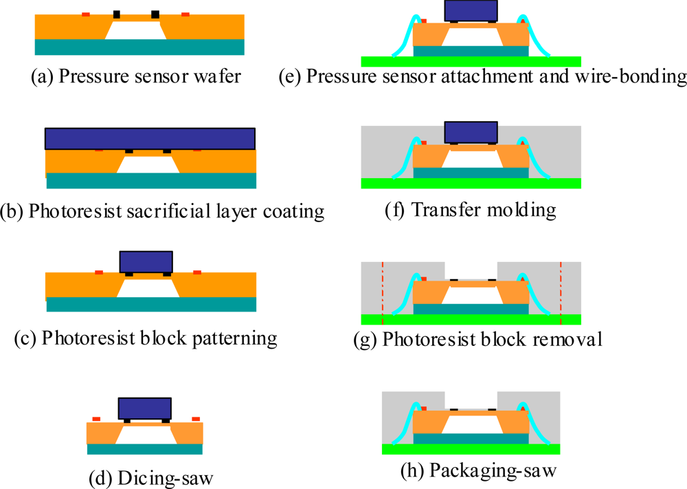
2.3.1. Sacrifice-replacement approach
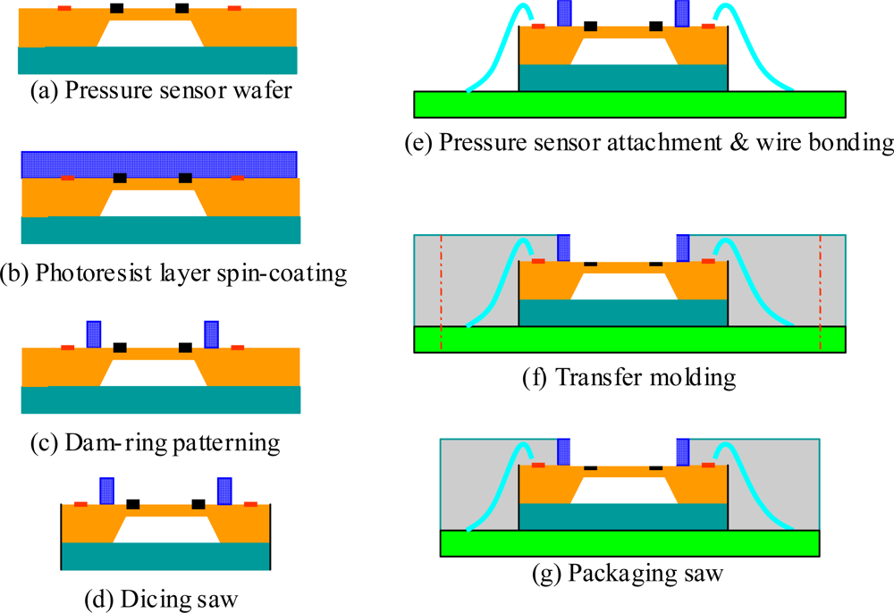
2.3.2. Dam-ring approach
3. Finite Element Analyses
3.1. Calculation of the Signal Output
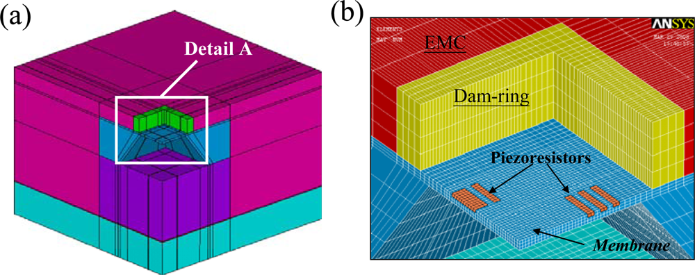
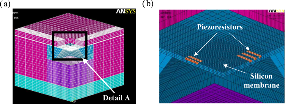
3.2. FE models of the Packaging
4. Results and Discussion
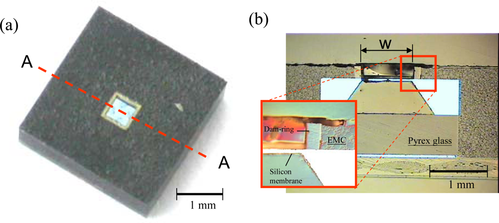
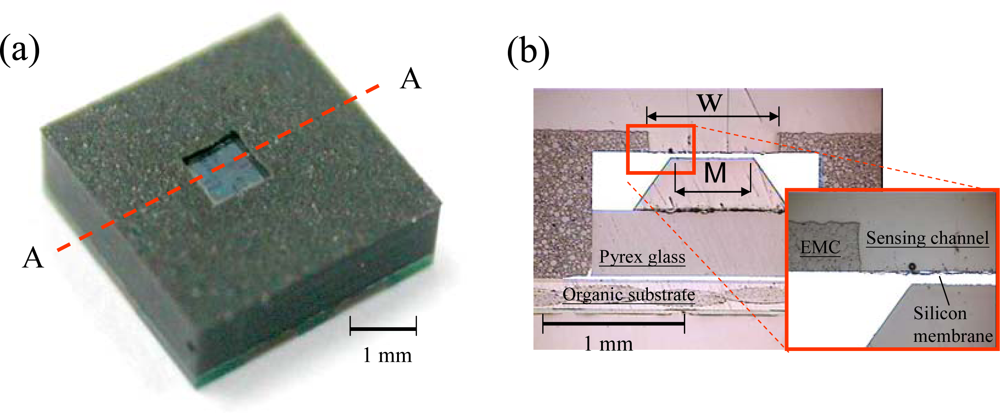
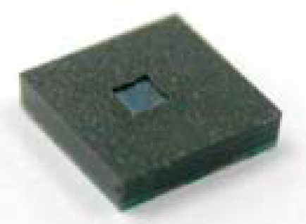
4.1. Packaged Pressure Sensors
4.1.1. Sacrifice-replacement approach
4.1.2. Dam-ring approach
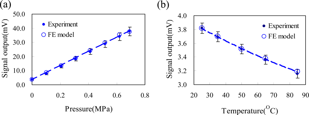
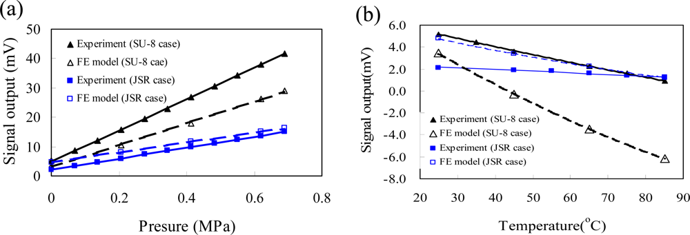
4.2. Validation of the FE Models
4.3. Characterization
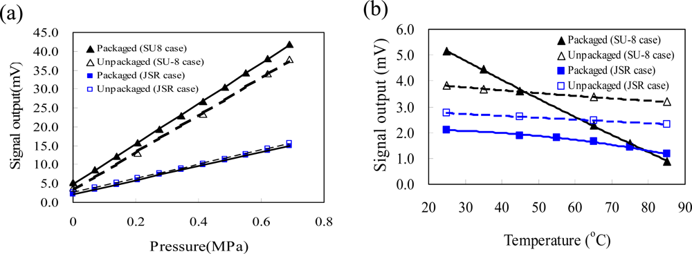
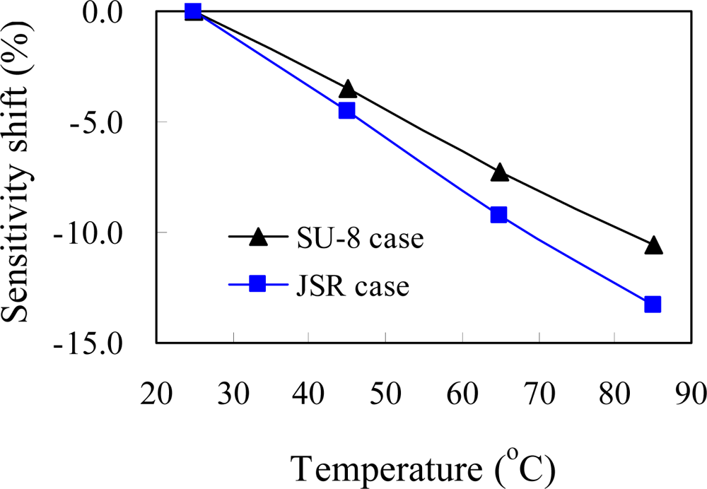
4.3.1. Packaging effect
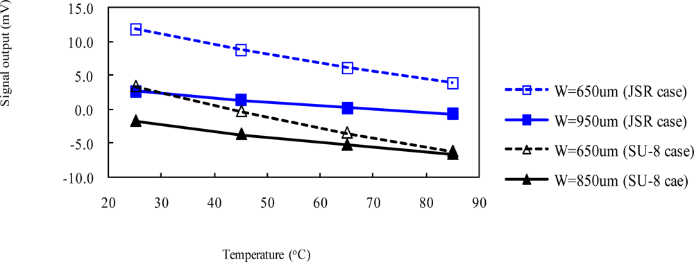
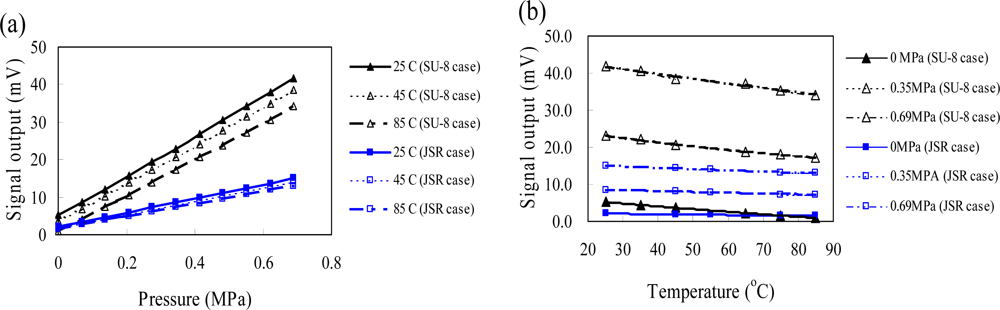
4.3.2. Comparison of packaging approaches
5. Conclusions
References
- Janczek, T. Material investigation for pressure sensor package p-dsof-8-1. Proceedings of the IEEE International Symposium on Polymeric Electronics Packaging, Norrkoping, Sweden, October 1997; pp. 220–222.
- Abbaspour-Santi, E.; Afrang, S.; Teymoori, M.M. A novel method for packaging of micromechined piezoresistive pressure sensor. Proceedings of the IEEE the International Conference on Software Engineering, Orlando, FL, USA, May 2002; pp. 141–144.
- Bitko, G.; Monk, D.J.; Maudie, T.; Stanerson, D.; Wertz, J.; Matkin, J.; Petrovic, S. Analytical techniques for examining reliability and failure mechanism of barrier coating encapsulated silicon pressure sensor exposed to harsh media. Proceedings of the SPIE, Austin, TX, USA, August 1996; pp. 248–258.
- Nyather, J.B.; Larsen, A.; Liverod, B.; Ohlckers, P. Measurement of package-induced stress and thermal zero shift in transfer molded silicon piezoresistive pressure sensors. J. Micromech. Microeng 1998, 8, 168–171. [Google Scholar]
- Dancaster, J.; Kim, W.; Do, D. Two-chip pressure sensor and single conditioning. Proceedings of the 12th International Conference on Solid-State Sensors, Actuators and Microsystems, Boston, USA, June 2003; pp. 1699–1702.
- Krondorfer, R.; Kim, Y.K.; Kim, J.; Gustafson, J.K.; Lommasson, T.C. Finite element simulation of packaging stress in transfer molded MEMS pressure sensors. Microelectron. Reliab 2004, 44, 1995–2002. [Google Scholar]
- Campabadal, F.; Cmeras, L.; Arrieta, M.J. Packaging of silicon pressure sensors for home application. Proceedings of the IEEE Conference on Electron Devices and Solid-State Circuits, Hong-Kong, China, December 2005; pp. 589–591.
- Krondorfer, R.; Kim, Y.K. Packaging effect on MEMS pressure sensor performance. IEEE Trans. Compon. Packag. Technol 2007, 30, 285–293. [Google Scholar]
- Cotofana, C.; Bossche, A.; Kaldenberg, P.; Mollinger, J. Low-cost plastic sensor packaging using the open-window packaging concept. Sens. Actuat. A: Phys 1998, 67, 185–190. [Google Scholar]
- Tseng, H.K.E; Zong, Z.B.; Lee, S.G.; Ho, S.C.; Srikanth, N. Development of transfer molding technology for package with die active side partially exposed. Proceedings of the 53th Electronic Components and Technology Conference, New Orleans, LA, USA, May 2003; pp. 365–372.
- Hsu, C.Y.; Chen, L.T.; Chang, J.S.; Chu, C.H. A novel packaging process for open-channel sensors. Proceedings of the International Microsystems, Packagings, Assembly and Circuits Technology Conference, Taipei, Taiwan, October 2007; pp. 258–261.
- Chen, L.T.; Hsu, C.Y.; Chang, J.S.; Shieh, W.L.; Xie, Y.Z.; Chu, C.H. A tiny plastic package of piezoresistive pressure sensors constructed by sacrifice-replacement approach. Proceedings of the 58th Electronic Components and Technology Conference, Lake Buena Vista, FL, USA, May 2008; pp. 1849–1854.
- Chen, L.T.; Cheng, W.H. A novel plastic package for pressure sensors fabricated using the lithographic dam-ring approach. Sens. Actuat. A: Phys 2009, 149, 165–171. [Google Scholar]
- Smith, C.S. Piezoresistance effect in germanium and silicon. Phys. Rev 1954, 94, 42–49. [Google Scholar]
- Roth, S.; Dellmann, L.; Racine, G.A.; Rooij, N.F. High aspect ratio UV photography for electroplated structure. J. Micromech. Microeng 1999, 9, 105–108. [Google Scholar]
- Brunet, M.; O’Donnell, T.; O’Brien, J.; McCloskey, P.; Mathuna, S.C.Ó. Thick photoresist development for the fabrication of high aspect ratio magnetic coils. J. Micromech. Microeng 2002, 12, 444–449. [Google Scholar]
- Kukharenka, E.; Kraft, M. Reliability of electroplating mold with thick positive spr 220-7 photoresist. J. Mater. Sci. Mater. Electron 2003, 14, 319–322. [Google Scholar]
- Despont, M.; Lorenz, H.; Fahrni, N.; Brugger, J.; Renaud, P.; Vettiger, P. High-aspect-ratio ultrathick negative-tone near-UV photoresist and its applications for MEMS. J. Micromech. Microeng 1997, 7, 121–124. [Google Scholar]
- Tseng, F.G.; Yu, C.S. High aspect ratio ultra-thick micro-stencil by JSR THB-430N negative tone UV photoresist. Sens. Actuat. A: Phys 2002, 97–98, 764–770. [Google Scholar]
- Lee, K.Y.; LaBianca, N.; Rishton, S.A.; Zolgharnain, S.; Gelorme, J.D.; Shaw, J.; Chang, T.H.-P. Micromachining applications of a high resolution ultratick photoresis. J. Vac. Sci. Technol. B 1995, 13, 3012–3016. [Google Scholar]
- Lorenz, H.; Despont, M.; Vettiger, P.; Renaud, P. Fabrication of photoplastic high-aspect ratio micro-parts and micro-molds using SU-8 UV resist. Microsyst. Technol 1998, 4, 143–146. [Google Scholar]
- Tsai, M.Y.; Wang, C.T.; Hsu, C.H. The effect of epoxy molding compound on thermal/residual deformations and stress on IC packaging during manufacturing process. IEEE Trans. Compon. Packag. Technol 2006, 29, 625–635. [Google Scholar]
- Lee, C.C.; Peng, C.T.; Chiang, K.N. Packaging effect investigation of CMOS compatible pressure sensors using flip chip and flex circuit board technologies. Sens. Actuat. A: Phys 2006, 126, 48–55. [Google Scholar]
- Peng, C.T.; Lin, J.C.; Lin, C.T.; Chiang, K.N. Performance and package effect of a novel piezoresistive pressure sensor fabricated by front-side etching technology. Sens. Actuat. A: Phys 2005, 119, 28–37. [Google Scholar]
- Krondorfer, R.; Kim, Y.K. Packaging effect on MEMS pressure sensor performance. IEEE Trans. Compon. Packag. Technol 2007, 30, 285–293. [Google Scholar]
- Xu, J.; Zhao, Y.; Jiang, Z. Analysis of the packaging stress in monolithic multi-sensor. Proceedings of the 2nd IEEE International Conference on Nano/Micro Engineering and Molecular Systems, Bangkok, Thailand, January 2007; pp. 241–244.
- Nysether, J.B.; Larsen, A.; Liverod, B.; Ohlckers, P. Measurement of package-induced stress and thermal zero shift in transfer molded silicon piezoresistive pressure sensors. J. Micromech. Microeng 1998, 8, 168–171. [Google Scholar]


| Items Unit | Packaging dimensions | ||
|---|---|---|---|
| Sacrifice-replacement approach | Dam-ring approach | ||
| Packaging size | mm3 | 4.0 × 4.0 × 1.5 | 4.0 × 4.0 × 1.5 |
| Sensing channel opening (w) | μm | 950 | 650 |
| Sensing channel depth | μm | 150 | 150 |
| Silicon membrane size (h) | μm2 | 576 × 576 | 576 × 576 |
| Silicon membrane thickness | μm | 20 | 30 |
| Freescale (MPXHZ6130) | Metrodyne (MPS-3100) | BOSCH (SMD085) | NSYSU (this study) | |
|---|---|---|---|---|
 |  |  |  | |
| Packaging size (mm) | 7.4 × 7.4 × 3.9 | 7.0 × 7.0 × 4.0 | 8.4 × 6.9 × 4.6 | 4.0 × 4.0 × 1.5 |
| Packaging volume | 7.8 | 7.0 | 8.8 | 1.0* |
© 2009 by the authors; licensee MDPI, Basel, Switzerland This article is an open access article distributed under the terms and conditions of the Creative Commons Attribution license (http://creativecommons.org/licenses/by/3.0/).
Share and Cite
Chen, L.-T.; Chang, J.-S.; Hsu, C.-Y.; Cheng, W.-H. Fabrication and Performance of MEMS-Based Pressure Sensor Packages Using Patterned Ultra-Thick Photoresists. Sensors 2009, 9, 6200-6218. https://doi.org/10.3390/s90806200
Chen L-T, Chang J-S, Hsu C-Y, Cheng W-H. Fabrication and Performance of MEMS-Based Pressure Sensor Packages Using Patterned Ultra-Thick Photoresists. Sensors. 2009; 9(8):6200-6218. https://doi.org/10.3390/s90806200
Chicago/Turabian StyleChen, Lung-Tai, Jin-Sheng Chang, Chung-Yi Hsu, and Wood-Hi Cheng. 2009. "Fabrication and Performance of MEMS-Based Pressure Sensor Packages Using Patterned Ultra-Thick Photoresists" Sensors 9, no. 8: 6200-6218. https://doi.org/10.3390/s90806200