Article

Optical and Surface Characterization of Radio Frequency Plasma Polymerized 1-Isopropyl-4-Methyl-1,4-Cyclohexadiene Thin Films

Electronic Materials Research Laboratory, School of Engineering and Physical Sciences, James Cook University, Townsville 4811, Australia
*
Author to whom correspondence should be addressed.
Electronics 2014, 3(2), 266-281; https://doi.org/10.3390/electronics3020266
Submission received: 21 February 2014 / Accepted: 14 April 2014 / Published: 23 April 2014
(This article belongs to the Special Issue Organic Semiconductors)

Abstract

:
Low pressure radio frequency plasma-assisted deposition of 1-isopropyl-4-methyl-1,4-cyclohexadiene thin films was investigated for different polymerization conditions. Transparent, environmentally stable and flexible, these organic films are promising candidates for organic photovoltaics (OPV) and flexible electronics applications, where they can be used as encapsulating coatings and insulating interlayers. The effect of deposition RF power on optical properties of the films was limited, with all films being optically transparent, with refractive indices in a range of 1.57–1.58 at 500 nm. The optical band gap (Eg) of ~3 eV fell into the insulating Eg region, decreasing for films fabricated at higher RF power. Independent of deposition conditions, the surfaces were smooth and defect-free, with uniformly distributed morphological features and average roughness between 0.30 nm (at 10 W) and 0.21 nm (at 75 W). Films fabricated at higher deposition power displayed enhanced resistance to delamination and wear, and improved hardness, from 0.40 GPa for 10 W to 0.58 GPa for 75 W at a load of 700 μN. From an application perspective, it is therefore possible to tune the mechanical and morphological properties of these films without compromising their optical transparency or insulating property.

1. Introduction

The latest advances achieved in the field of organic electronics have expanded the scope of applications beyond those attainable with conventional silicon (Si) semiconducting technologies to include flexible photovoltaic (PV) and light-emitting devices, flexible displays, chemical and biological sensors, wearable and implantable electronics, to name a few [1,2,3,4,5,6,7]. Among these, organic thin film photovoltaics (OPV) is an emerging economically-competitive PV technology that combines manufacturing adaptability, low-cost processing and a lightweight, flexible device end-product. In spite of the significant advances in OPV, commercial use of this technology remains limited, due to both low power conversion efficiency (PCE) and poor overall stability of the devices. Indeed, even though the highest PCE achieved from organic PV has risen from 2.5% to 11% for bulk heterojunction polymer: fullerene solar cells over the last ten years, it falls short of 25%–30% PCE level offered by established Si photovoltaic cells. The lifetime achievable by the most advanced organic solar cells is also far below the 20–25 years lifespan of commercial Si photovoltaic cells [8], attributed to relatively low environmental stability of organic photoactive materials.
Most of the research effort to date has concentrated around the photoactive layer, focusing on new, more efficient and stable materials with tailored energy levels and solubility, and a better understanding of the mechanism of photon–to–electron conversion [9]. However, encapsulation with high barrier performance materials has also been recognized as instrumental in significantly improving device lifetime, where device stability is extended by limiting penetration of oxygen and moisture from the environment into device layers [10]. For instance, encapsulation of solar cells based on coating of ZnO layer on top of a photoactive material and subsequent UV resin drop coating resulted in a significant increase in the stability, shelf life of the device, and the cost-effectiveness [11]. Recently synthesized silicon oxide/alumina and parylene layer had an effective water vapor transmission (WVTR) rate of 2.4 ± 1.5 × 10⁻⁵ g/m2/day [12]. However, the requirements for high performance encapsulation materials include good processability, high optical transmission, high dielectric constant, low water absorptivity and permeability, high resistance to ultra-violet (UV) degradation and thermal oxidation, good adhesion, mechanical strength, and chemical inertness [13]. While inorganic barrier layers are often used for their sound durability [14], organic encapsulation materials are attracting attention for their synthetic flexibility and resulting property tunability [15].
Organic thin film materials fabricated from renewable precursors using low-cost deposition methods, such as plasma-assisted nanoassembly, have lower environmental and economic costs [16]. Low-temperature plasma deposition is a highly engineering-friendly, economical method of polymer synthesis, that delivers practically pollutant free surface chemistry, and can be easily integrated into manufacturing processes [17,18]. The method offers a level of confidence and deposition quality comparable to and in many cases superior to other widely-used techniques, such as thermal chemical vapor deposition, wet chemistry processing, laser assisted microfabrication, etc. [19,20]. Films fabricated using plasma-assisted synthesis are typically smooth, ultrathin and pinhole free, with good spatial uniformity, conformal coverage, and high adhesion to the substrate [21].
1-isopropyl-4-methyl-1,4-cyclohexadiene, also known as γ-terpinene, is a non-synthetic isomeric hydrocarbon derived from Melaleuca alternifolia essential oil. Earlier, Jacob and co-workers have successfully used plasma-assisted deposition to fabricate thin films from other renewable precursors for application in electronics and biomedical fields, reporting property variability linked to both deposition conditions and the chemistry of the monomer [22,23,24,25,26]. This paper reports on the plasma-assisted fabrication of new polymer thin films from γ-terpinene, with intention to use these films in OPVs, specifically as encapsulation coatings, and as insulating layers in flexible electronics. Given the proposed application for the plasma polymerized γ-terpinene (pp–GT), the material is studied in terms of optical, surface, mechanical, and adhesion properties as a function of deposition conditions.

2. Experimental Section

Thin film samples were deposited on high quality glass microscope slides inside a custom made, cylindrical RF polymerization chamber, 0.75 m in length with an inner diameter of 0.055 m (approximate volume of 0.018 cm3). The slides were thoroughly cleaned using extran, an ultrasonic bath of distilled water, and rinsed with isopropanol prior to deposition. Using the procedure outlined in [22], plasma polymer films were fabricated from γ-terpinene monomer (Figure 1) at various input RF power levels (10, 25, 50 and 75 W) and at an ambient temperature of 20 °C. The monomer flow rate was estimated to be 1.57 cm3/min by employing the procedure outlined by Gengenbach and Griesser [27].
Figure 1. Chemical structure of 1-Isopropyl-4-methyl-1,4-cyclohexadiene (C10H16).
Electronics 03 00266 g001
Variable angle spectroscopic ellipsometry (VASE) measurements were performed using a J.A. Woollam Co. Inc. model M-2000D variable angle spectroscopic ellipsometer to estimate sample thickness and optical properties of pp–GT thin films [28]. The refractive index n, extinction coefficient k and thickness were derived from the experimental Δ and Ψ data via regression analysis. The relation between n and thickness for the polymer samples has also been investigated. UV-Vis spectroscopy measurements were performed using an Avantes Avaspec-2048 spectroscopy unit with an Avalight-DHc light source to measure the absorbance in the ultraviolet and visible region. From those data, values of optical band gap have been derived. Surface morphology and roughness parameters of pp–GT thin films fabricated under different RF powers were determined from atomic force microscope (AFM) images acquired on a NT-MDT NTEGRA Prima AFM operating in semi-contact mode. A Hysitron Triboscope was used to perform the nanoindentation study. During the nanoindentation study, a Berkovich indenter (70.3° equivalent semi-opening angle) was used and instrument compliance was calibrated using fused silica. Preliminary images of the samples under investigations were collected in order to evaluate the roughness of the area to be indented. Twelve indentations were made on each sample and the results presented are an average of these indentations. Typical loads used in the indentation ranged from 100 μN to 2000 μN with fixed loading time and hold time of between 2 and 5 s.
In the load-partial unload (PUL) experiment, several cycles of loading and unloading were performed in a sequence (Figure 2). At a constant rate of loading and unloading (100 μN/s), the Berkovich indenter was first loaded and unloaded two times in succession with each of the unloadings terminated at 10% of the maximum load to assure the contact between the pp–GT thin film sample and the indenter. This was performed to examine the reversibility of the deformation and thus ensure that the unloading data used for analysis purposes were mostly elastic [29]. The load was held constant after the second unloading for a fixed period of time at 10% of the peak value while the displacement was carefully monitored to establish the rate of displacement produced by thermal expansion in the system. Following the hold period, the sample was loaded for the last time to allow any final time dependent plastic effects to diminish, with another fixed hold period inserted at peak load and then the specimen was fully unloaded.
Figure 2. Typical load–time sequence used for load–partial unloading experiments.
Electronics 03 00266 g002
After the indentations were performed, stiffness values and the known modulus for quartz were used to calculate the contact area for each indent. Contact parameters and mechanical properties of the pp–GT thin films are derived from the contact area and load-displacement curve as proposed by Oliver and Pharr [29]. The unloading stiffness was determined after polynomial fitting of 90% of the unloading curve.
The cross-hatch test was performed on pp–GT films fabricated at different power levels using the Elcometer 107 kit to obtain a standardized (ASTM D3359) qualitative assessment of the adhesion between the films and the glass substrate. Crosshatch patterns were made on the polymer film surfaces using the cutting tool (6 teeth, 1 mm spacing). The whole area was then brushed to remove debris and adhesive tape was applied on top of the lattice followed by smoothing out the tape with a pencil eraser across the surface. The tape was then removed by pulling at an angle of 180° and the results were analyzed by comparing the lattice of cuts with ISO standards. Three samples were fabricated for each applied RF power, with three crosshatch tests performed on each sample.

3. Results and Discussion

3.1. Effect of Time on Film Thickness

The dependence of pp–GT thin film thickness on the deposition time was studied on samples fabricated for 2, 5, and 10 min at 25 W RF power along with constant monomer flow rate and pressure. A film thickness of 120 nm was obtained with deposition time of 2 min at 25 W. The sample thickness increased linearly with time, approaching 438 nm for deposition time of 10 min. Similar trend was observed for films fabricated at 10, 50, and 75 W RF power. Film thickness is also found to be linearly increasing with higher RF power. This is due to an increase in the densification of electrons with an increased crosslinking. Same phenomenon has also been observed in case of plasma polymerized terpinen-4-ol and linalyl acetate (PLA) thin films [26,30]. Assuming constant deposition conditions (pressure, monomer flow rate, distance between electrodes, etc.), the desired film thickness of pp–GT thin film for a potential application can therefore be achieved by controlling the time of deposition.

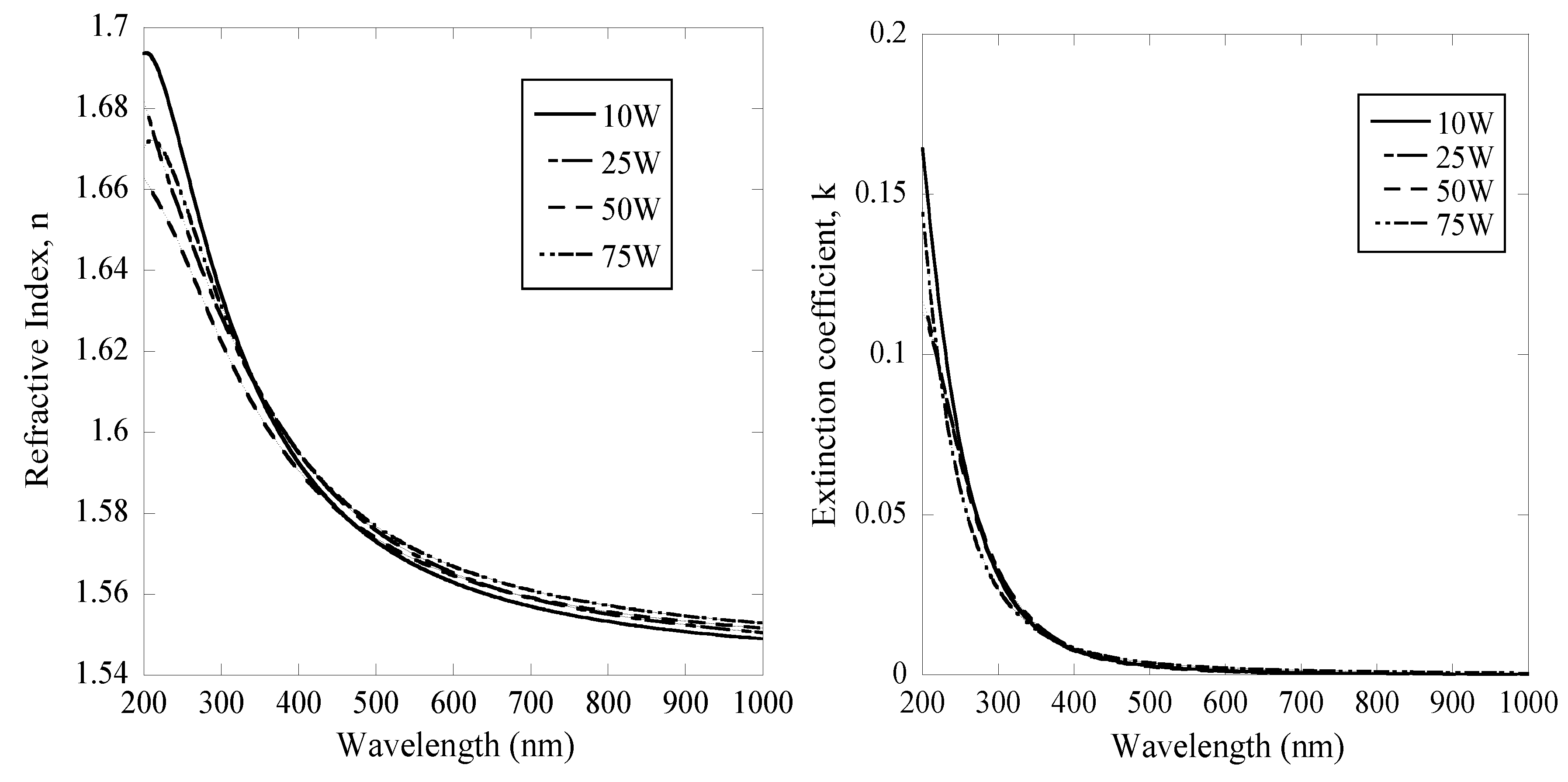
3.2. RF Power Dependence of Optical Constants

The effect of changing the RF power level on the optical constants of pp–GT polymer thin films has been studied using VASE and UV-Vis spectroscopy over the wavelength range of 200–1000 nm. UV-Vis absorption spectrums of samples fabricated at 10, 25, 50, and 75 W RF power level (Figure 3) reveal that the absorption contour is replicable over the RF power range employed during fabrication. Reallocating of the peak position and/or broadening of the peak are not observed with increase in RF power, unlike other studies [31]. The maximum absorption of pp–GT films fabricated at different RF power levels is found to be at 300 nm. It is believed that the main absorption peak may be the result of pi–pi * transitions. The optical transparency of the polymer films is confirmed by these spectra as the maximum absorption peaks are outside of the visible region of the spectrums. The optical transparency of the pp-GT film can be effectively used in applications such OPV, medical imaging, optical sensor and as an encapsulating (protective) layer for the electronic circuits.
Figure 3. UV-Vis absorption spectrum of pp–GT thin films.
Electronics 03 00266 g003
Figure 4 demonstrates the n and k profiles of pp–GT thin films fabricated at various power levels. Thickness and surface roughness parameters from Cauchy analysis (WVASE software) were used to obtain n and k profiles. Mean squared error (MSE) values used to assess the quality of the modeling fit were below 3. Considering the profiles, it is observed that the overall shape of the curves was similar across all the samples. At short wavelengths (below 250 nm), a sharp peak in n profile was detected. At wavelengths above approximately 250 nm, an increase in RF input power resulted in higher n values for the polymer. At 500 nm, the difference in refractive index between 10 and 75 W sample is 0.01, corresponding to a change of less than 1% that is similar to thin films fabricated from linalyl acetate [32].
Figure 4. Refractive indices and extinction coefficient of pp–GT thin films.
Electronics 03 00266 g004
Based on the refractive index values of pp–GT films, it is anticipated that it can be used as a coating on long-period fiber gratings (LPFGs) to enhance its sensitivity, similar to δ-form syndiotactic polystyrene [33]. According to [34], pp–GT can also be used in advanced optoelectronic fabrications, such as high performance substrates for advanced display devices, optical adhesives or encapsulants for OPV devices, antireflective coatings for advanced optical applications or image sensors [4,5,10].
The extinction coefficient (k) profiles for pp–GT samples fabricated at various RF power levels illustrate very similar characteristics. These results (optical similarities with glass and transparency in the visible wavelength region) confirm pp–GT thin films as a strong candidate for use as encapsulation coatings in OPV, optical devices, such as LEDs, FETs, and lenses.
Abbe number (vD), a key parameter for the refractive index dispersion, is of great importance for optical materials used in the visible region. It is also defined as v-number or refractive efficiency or constringency of the material. The Abbe number is given by following equation [35]:
Electronics 03 00266 i001
where nd, nF, and nC are the refractive indices of the material at the wavelengths of sodium D (587.6 nm), hydrogen F (486.1 nm), and hydrogen C (656.3 nm), respectively [35]. Materials that have a higher Abbe number (vD) have lower dispersion in the refractive index, whereas highly refractive materials have small Abbe numbers [36,37]. A polymer having low vD (<30), is therefore not suitable for use in optics [36].
For pp–GT films, vD increases from 35.37 to 40.35 (Table 1) with increase in RF power (10 W to 75 W), which confirms that films fabricated at 75 W have lower dispersion in the refractive index. These results indicate the well-balanced properties and hence the pp–GT polymer thin films are potential candidates for advanced optical applications.
Table 1. Abbe-numbers for pp–GT thin films.
RF Power (W)vD
1035.37
2535.18
5037.80
7540.35

3.3. Thickness Dependence of Optical Constants

Thickness dependence study was carried out using spectroscopic ellipsometry data taken for pp–GT thin films fabricated at 25 W with different film thicknesses and the corresponding n and k profiles. With an increase of thickness over the measured wavelength region, a very small increase of n is observed. The shift in n vs. thickness is comparable to that found for polyparaxylene films [38], which were deemed to not have significant thickness dependence on n. The shifts found in pp–GT thin films are therefore insignificant and thus n is not dependent on thickness.

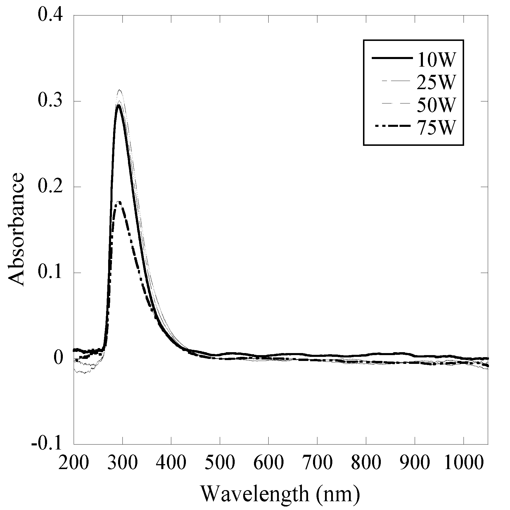
3.4. Determination of the Energy Gap

To determine the nature of the optical transitions, the optical absorption study was performed for pp–GT thin films. The optical absorption coefficient data were obtained from UV–Vis spectroscopy measurements. The optical absorption dependence of photon energy is expressed by the following relationship [39]:
αhv = A(hvEg)m
where A is an energy-independent constant, Eg is the optical band gap and m is a constant which is connected to the density-of-states distribution in the transport gap in the band tails and thus determines the type of transition (m = 1/2 and 3/2 for direct allowed and forbidden transitions, respectively, m = 2 and 3 for indirect allowed and forbidden transitions, respectively) [39].
The optical absorption coefficient data obtained from UV-Vis spectroscopy measurements were converted to a Tauc plot using a MATLAB program. In that curve, a value of m = 3/2 was employed for all the pp–GT thin films studied, as this value provided the most linear plot, indicating direct forbidden transitions. The indirect process is much slower than the direct transitions as it requires three entities to intersect in order to proceed: an electron, a photon, and a phonon. Materials showing direct transition are therefore much more efficient than materials that show indirect transition. Gallium arsenide (GaAs) and other direct band gap materials are used in optical devices, such as LEDs and lasers, whereas Si that is an indirect band gap material is not used. This study shows that pp–GT, having direct transition has the potential to be used in different optical devices. The optical band gap values (Table 2) remained between 3.14 eV and 3.01 eV, falling within the insulating region of Eg. The pp–GT thin films can therefore be used as insulators for the application of flexible coating on electrical apparatus (e.g., printed circuit board, high voltage systems, circuit breakers, etc.).
Table 2. Optical bandgap of pp–GT thin films for m = 3/2.
RF power (W)Eg (eV)
103.14
253.08
503.07
753.01

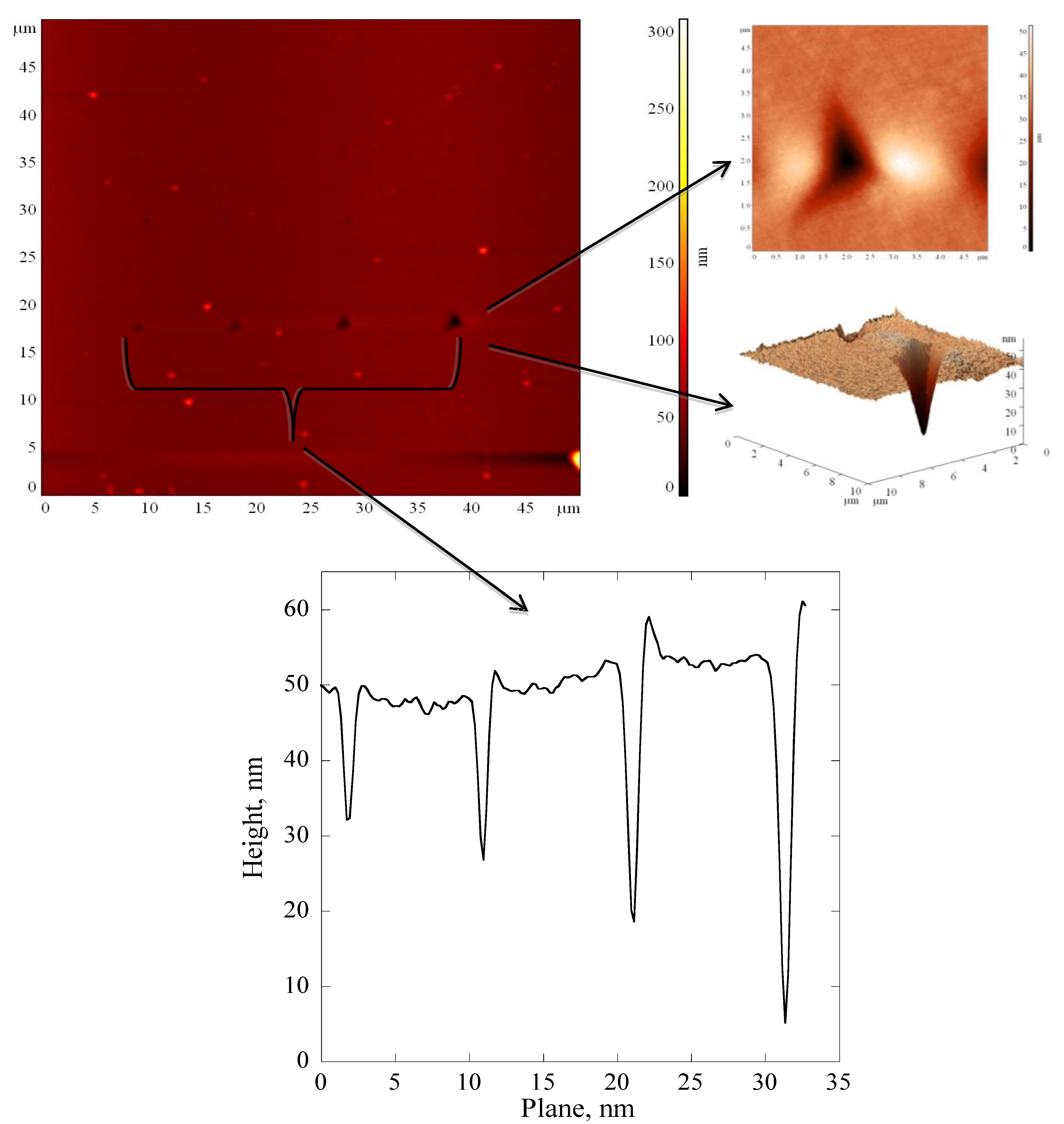
3.5. Surface Morphology
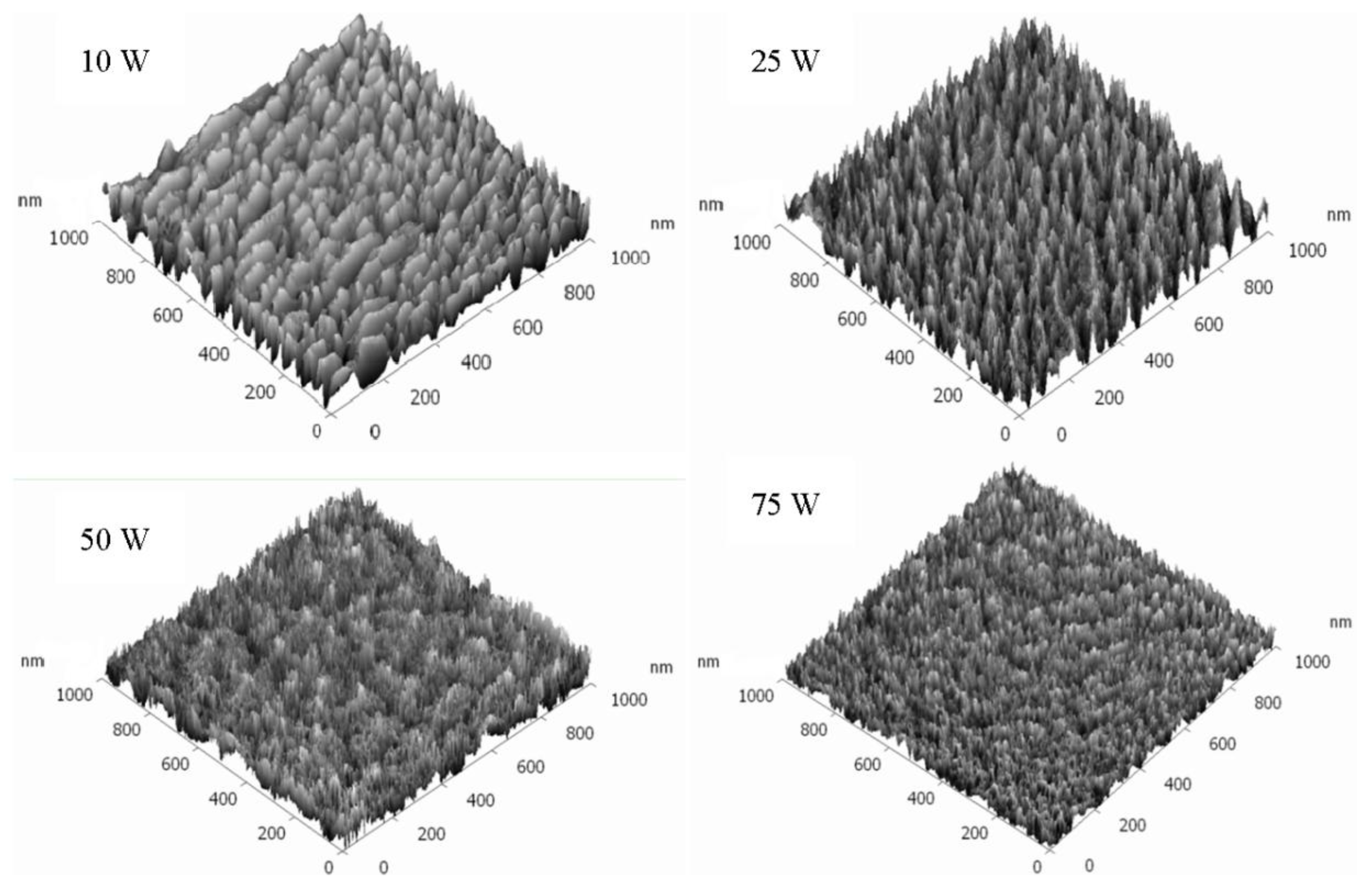
The surface profile of pp–GT thin films fabricated at various input RF power levels were studied to examine surface defects and roughness The topographical features of the investigated films deposited on glass surfaces are shown in Figure 5.
Figure 5. AFM images of pp–GT thin films fabricated at 10, 25, 50, and 75 W input RF power levels.
Electronics 03 00266 g005
From this study, pp–GT thin films are found to be smooth, uniform and defect-free, exhibiting consistent morphology across film samples. Average roughness values for all samples were approximately 0.3 nm. These roughness values were in agreement with the roughness values found by means of spectroscopic ellipsometry. I Surfaces with RMS roughness values below 0.5 nm have an insignificant effect on its surface and chemical properties and performance [40]. Considering this and the determined roughness of 0.3 nm, the polymerization reactions are confirmed to take place mostly on the surface of the glass substrate rather than in the gas phase [41].
Beside the conventional roughness parameters Ra and Rq, the statistical parameters, such as Rsk (skewness) and Rkur (kurtosis), were determined for the pp–GT thin films. Rkur is a quantitative measure of the kurtosis, which is defined as the randomness of profile heights that determines whether the data sets are peaked or flat relative to a normal distribution. Rkur values can range from 0 to 8. Surfaces with distinct peaks that decline rather rapidly and have heavy tails exhibit high values; whereas rough surfaces with flat top near the mean possess lower values. The pp–GT thin film fabricated at 10 W has lower value of Rkur (Table 3), whereas sharp peaks and heavier tails are found for samples fabricated at higher RF power levels (Figure 5) that have relatively high values of Rkur (Table 3). A surface skewness (Rsk) greater than 0 is observed for pp–GT films, i.e., the predominance of disproportionate number of peak-like surface features. Furthermore, it was observed that the 75 and 50 W samples have smaller and tapered features (narrow curves) while the 25 and 10 W samples have broad curves. Furthermore, decrease in entropy indicates the surface flatness, i.e., reduction of growth of pores at higher RF power levels [42]. Because of this behavior, Rrms and Ra values decreased with increase of RF power. However, higher deposition rate of pp–GT resulted in an increase in the surface roughness values due to the fact that the particles in the growth region were unable to relax fast enough before the next layer of the film is deposited [43]. These surface analysis results clearly indicate the difference between the peak distributions for pp–GT samples fabricated at different RF power that may affect the wettability. Uniformity of films is also confirmed from the analysis, which indicates the less prone to fracture characteristics of the pp–GT films.
Table 3. Roughness parameters of pp–GT thin films.
Roughness parameters10 W25 W50 W75 W
Maximum peak height Rmax (nm)4.482.382.162.15
Average roughness Ra (nm) 0.300.280.250.21
Root mean square Rq (nm)0.390.340.320.30
Surface skewness Rsk0.320.220.140.08
Coefficient of kurtosis Rkur0.060.540.630.77
Entropy 6.124.53.93.56
Surface morphology can also be described in relation to the wetting behavior of the plasma films. Surface roughness generally enhances the hydrophilicity [44]. For pp–GT thin films, the decrease in roughness values with higher deposition power is therefore considered to contribute to the increased hydrophobicity of the surface. Smooth surfaces with greater hydrophobicity are vital for optical and electrical applications, and also for implementing as coating materials for surface protection or buffer layers [45].

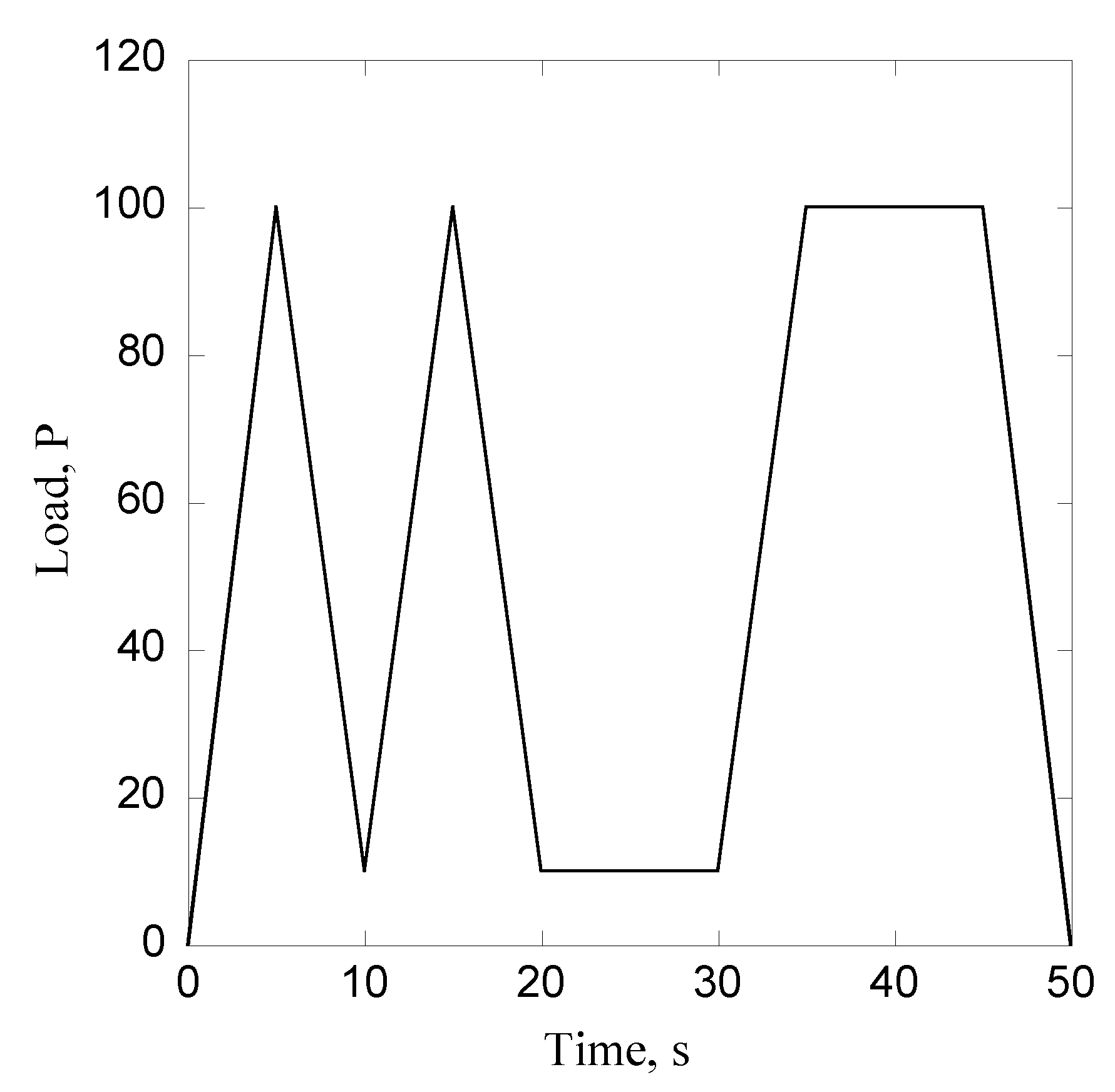
3.6. Nanoindentation
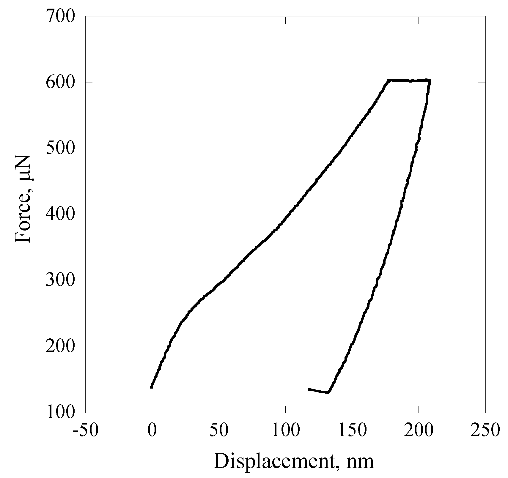
Mechanical properties of pp–GT deposited under different RF power conditions were investigated using a single indentation method and a load‐partial unload technique. A series of indentations were made in the films with depths ranging from 221.5 nm to 207.2 nm depending on the thickness of the film. Illustrative single indentation curves from 2 μm thick pp–GT film fabricated at 10 W is presented in Figure 6.
The load-unload curve (Figure 6) shows the typical behavior of pp–GT thin films undergoing a nanoindentation test. The initial slope of the unloading process is used to deduce the reduced elastic modulus of the material at the specific contact depth, hc. There are a number of pop-ins in the curve initially and this phenomenon may be attributed to micro-cracking or dislocation nucleation and/or propagation during loading as have been investigated in a wide variety of materials [46].
Figure 6. Load–displacement diagram of pp–GT thin film fabricated at 10 W.
Electronics 03 00266 g006
The elastic moduli and hardness of different pp–GT thin film samples increased with the increasing RF power as seen from Table 4. Elastic modulus of pp–GT thin film fabricated at 10 W is 4.22 GPa, while film fabricated at 75 W reaches an elastic modulus of 5.96 GPa. Increase in modulus is also observed with decreasing hc. This may be due to the transition from spherical contact to conical contact behavior occurred at hc = indenter radius/4 for the Berkovich indenter used in the study [47]. Data at lower depths should be treated with caution as the contact modulus measured varies considerably with tip radius under spherical contact conditions. Hardness of pp–GT thin films also follows the same trend as elastic modulus. The hardness of the materials increases with increase in input RF power and this can be attributed to the higher crosslinking of the polymers fabricated at higher power levels [22]. This results in an increase in resistance against sample deformation. Increase of elastic modulus and hardness with increasing RF power has also been reported in other materials such as linalyl acetate [26]. However, it should be noted that several sources of error may exist in these experiments, which may include the relative non-uniformity of the indent (e.g., pile-up and sink-in phenomena) observed on some samples, and difficulties in precise estimation of the indent area (e.g., possible overestimation in the case of pile-up and underestimation due to sink-in features), respective influences of material properties and sample thicknesses and creep [48]. In addition, artifacts and tip effects affecting the precision of the measurement may possibly be imaged due to the usage of same tip for the actual indentation process and imaging. In a nanoindentation test, very often the stress relaxation is observed at the maximum load during unloading process. This is due to the large strain beneath indenter and the large strain rate at this point (since the loading rate is usually finite during the experiment). Moreover, sudden withdraw of indenter causes oscillations in measurement whereas holding at maximum load may lead to uncertainties in the measured quantities [48]. In addition, the initial portion of unloading is more prone to thermal drift than the loading curve. The values presented in Table 4 are therefore indicative of the evolution of the hardness properties of pp–GT thin films under changing fabrication conditions and may quantitatively differ from the actual material properties due to aforementioned measurement bounds.
Table 4. Hardness parameters of pp–GT thin films.
RF power (W)Contact depth, hc (nm)Hardness, H ± SE (GPa)Final depth, hf (nm)Elastic modulus, E (GPa)
10221.50.40 ± 0.01137.904.22
25218.30.46 ± 0.02102.534.61
50211.70.51 ± 0.0283.604.90
75207.20.58 ± 0.0369.765.96
Loading time and holding time have significant effect on the indentation behavior of pp–GT thin films. To investigate these effects, single indentations were performed on samples deposited at 75 W at constant load of 1000 μN. Figure 7 shows typical repeat single indentation profiles under increasing indentation load of pp–GT film deposited at 75 W. Hardness value decreased from 0.57 GPa to 0.53 GPa with increasing loading and unloading time with rates (r) ranging from 0.5 to 20 nm/s. As creep deformation taking place during the holding time influences the contact depth at maximum load, the hardness values obtained using these maximum contact depth estimates will also be affected [24]. Moreover, the holding time at maximum load affects the unloading portion of the load displacement curve. In this study, an increase in the hold time showed a decrease in the positive slope value of the material. The relationship of decrease in this slope of unloading in the load-displacement curve and modulus of the pp–GT thin films can be explained by the following equation [49]:
Electronics 03 00266 i002
The decrease in the slope value means decrease in the dP/dh value that leads to a decrease in modulus value. Further increase in hold time increases the indentation depth of the indenter tip on the thin film surface, which leads to increase in contact area of the indenter with the film. The increase in the contact area decreases the hardness of the film. In the case of pp–GT thin films, increasing the hold time from 5 to 25 s at constant load of 500 μN resulted in a decrease in the calculated hardness from 0.59 to 0.53 GPa.
To extend the capabilities of quasistatic testing to allow depth profiling of pp–GT thin films, the partial unloading (PUL) technique was used. This investigation revealed that at depths below 190 nm (2 μm thick pp–GT film), the depth profile of the hardness follows a trend similar to that determined using the single indentation approach. The hardness of the system gradually increases above approximately 190 nm due to the stress field no longer being contained within the body of the thin film.
Figure 7. Typical AFM image of plastic impressions remaining in pp–GT sample fabricated at 75 W after indentation under different load conditions.
Electronics 03 00266 g007

3.7. Adhesion Study

The adhesion behavior of pp–GT thin films deposited on glass is presented in Figure 8. The adhesion improved with higher deposition power. Films fabricated at 10 W showed 5%–15% delamination. However, films fabricated at 50 and 75 W showed no delamination effect with a higher cross hatch rating.
Figure 8. Adhesion data for pp–GT thin films at 10, 25, 50, and 75 W.
Electronics 03 00266 g008
The optical image acquired using the microscope and CCD camera for the 10 W sample showed a significant amount of deformation occurred to the sample upon applying and consequent removal of the adhesive tape. For the thin films deposited at 25 W, the areas that were not affected by the tape test appeared uniform and with the increasing of RF power, this uniformity increased. This trend is attributed to the interfacial bonding that is improved by an increase in cross-link density associated with increasing applied RF power. These findings provide an insight into the reliability of the pp–GT films.

4. Conclusions

The basic optical properties and optical constants of the pp–GT thin films were investigated by means of spectroscopic ellipsometry and UV-Vis spectroscopy. The optical constants such as the refractive index (n), extinction coefficient (k), and optical band gap were determined. The films are confirmed as optically transparent and independent of RF power. The refractive index and extinction coefficient of the pp–GT thin films demonstrated very little dependence on RF power and film thickness. The optical absorption spectra showed that the absorption mechanism is a direct transition. The independence of the refractive index on the RF power level demonstrates the pp–GT thin films as an impending optically stable material for optical applications.
AFM investigation demonstrated that the pp–GT films were smooth, uniform and defect-free. The average roughness parameter decreased with increasing RF power (0.30 for 10 W and 0.21 for 75 W). In the nanoindentation study, combined effects of loading rate and holding time were investigated. For the load rates and hold time considered, pp–GT thin films were found to be a function of both the variables. The unloading portion of the load-displacement curve was found to be strongly dependent on the holding time. The hardness increased from 0.40 GPa for 10 W to 0.58 GPa for 75 W at a load of 700 μN. Elastic modulus of pp–GT thin film fabricated at 10 W was found to be 4.22 GPa, while elastic modulus of 5.96 GPa was found for 75 W film. An adhesion study established that the quality of adhesion is improved for samples fabricated at higher RF power, while the films produced at low RF power adhered poorly to the substrates. These studies demonstrate that the pp–GT polymer is a potential candidate for thin film applications in flexible electronics and OPV that entail smooth and uniform surfaces.

Acknowledgments

JA is grateful to the financial support provided by the JCUPRS scholarship. KB acknowledges funding from JCU and ARC (DE130101550).

Conflicts of Interest

The authors declare no conflict of interest.

References

  1. Jung, K.; Choi, W.-K.; Chae, K.H.; Song, J.-H.; Yoon, S.-J.; Lee, M.-H.; Choi, J.-W. Highly conductive and damp heat stable transparent ZnO based thin films for flexible electronics. J. Alloys Compd. 2013, 554, 240–245. [Google Scholar] [CrossRef]
  2. Dubal, D.P.; Holze, R. All-solid-state flexible thin film supercapacitor based on Mn3O4 stacked nanosheets with gel electrolyte. Energy 2013, 51, 407–412. [Google Scholar] [CrossRef]
  3. Qian, X.; Wang, T.; Yan, D. Transparent organic thin-film transistors based on high quality polycrystalline rubrene film as active layers. Org. Electron. 2013, 14, 1052–1056. [Google Scholar] [CrossRef]
  4. Ferguson, A.J.; Blackburn, J.L.; Kopidakis, N. Fullerenes and carbon nanotubes as acceptor materials in organic photovoltaics. Mater. Lett. 2013, 90, 115–125. [Google Scholar] [CrossRef]
  5. Kelly, F.M.; Meunier, L.; Cochrane, C.; Koncar, V. Polyaniline: Application as solid state electrochromic in a flexible textile display. Displays 2013, 34, 1–7. [Google Scholar] [CrossRef]
  6. He, H.; Xu, X.-B.; Zhang, D.-F. An aligned macro-porous carbon nanotube/waterborne polyurethane sensor for the detection of flowing organic vapors. Sens. Actuators B: Chem. 2013, 176, 940–944. [Google Scholar] [CrossRef]
  7. Curto, V.F.; Fay, C.; Coyle, S.; Byrne, R.; O’Toole, C.; Barry, C.; Hughes, S.; Moyna, N.; Diamond, D. Real-time sweat pH monitoring based on a wearable chemical barcode micro-fluidic platform incorporating ionic liquids. Sens. Actuators B: Chem. 2012, 171–172, 1327–1334. [Google Scholar] [CrossRef] [Green Version]
  8. Krebs, F.C. Alternative PV: Large scale organic photovoltaics. Refocus 2005, 6, 38–39. [Google Scholar] [CrossRef]
  9. Su, Y.-W.; Lan, S.-C.; Wei, K.-H. Organic photovoltaics—Review article. Mater. Today 2012, 15, 554–562. [Google Scholar] [CrossRef]
  10. Ahmad, J.; Bazaka, K.; Anderson, L.J.; White, R.D.; Jacob, M.V. Materials and methods for encapsulation of OPV: A review. Renew. Sustain. Energy Rev. 2013, 27, 104–117. [Google Scholar] [CrossRef]
  11. Lee, H.-J.; Kim, H.-P.; Kim, H.-M.; Youn, J.-H.; Nam, D.-H.; Lee, Y.-G.; Leeb, J.-G.; Yusoffa, A.R.M.; Jang, J. Solution processed encapsulation for organic photovoltaics. Sol. Energy Mater. Sol. Cells 2013, 111, 97–101. [Google Scholar] [CrossRef]
  12. Kim, N.; Graham, S. Development of highly flexible and ultra-low permeation rate thin-film barrier structure for organic electronics. Thin Solid Films 2013, 547, 57–62. [Google Scholar] [CrossRef]
  13. Cuddihy, E.; Coulbert, C.; Gupta, A.; Liang, R. Electricity from Photovoltaic Solar Cells: Flat-Plate Solar Array Project Final Report. Volume VII: Module Encapsulation; Jet Propulsion Laboratory: 1986. Available online: http://resolver.caltech.edu/JPLpub86-31-volumeVII (accessed on 17 April 2014).
  14. Kim, N. Fabrication and Characterization of Thin-Film Encapsulation for Organic Electronics. Ph.D. Thesis, Mechanical Engineering, Georgia Institute of Technology, Atlanta, GA, USA, 2009. [Google Scholar]
  15. Spanggaard, H.; Krebs, F.C. A brief history of the development of organic and polymeric photovoltaics. Sol. Energy Mater. Sol. Cells 2004, 83, 125–146. [Google Scholar] [CrossRef]
  16. Shaheen, S.E.; Ginley, D.S.; Jabbour, G.E. Organic-Based Photovoltaics: Toward Low-Cost Power Generation. MRS Bull. 2005, 30, 10–19. [Google Scholar] [CrossRef]
  17. Forrest, S.R. The path to ubiquitous and low-cost organic electronic appliances on plastic. Nature 2004, 428, 911–918. [Google Scholar] [CrossRef]
  18. Vasilev, K.; Griesser, S.S.; Griesser, H.J. Antibacterial Surfaces and Coatings Produced by Plasma Techniques. Plasma Process. Polym. 2011, 8, 1010–1023. [Google Scholar] [CrossRef]
  19. Ostrikov, K.; Neyts, E.C.; Meyyappan, M. Plasma nanoscience: From nano-solids in plasmas to nano-plasmas in solids. Adv. Phys. 2013, 62, 113–224. [Google Scholar] [CrossRef]
  20. Michelmore, A.; Charles, C.; Boswell, R.W.; Short, R.D.; Whittle, J.D. Defining Plasma Polymerization: New Insight Into What We Should Be Measuring. ACS Appl. Mater. Interfaces 2013, 5, 5387–5391. [Google Scholar] [CrossRef]
  21. Rahman, M.J.; Bhuiyan, A.H. Structural and optical properties of plasma polymerized o-methoxyaniline thin films. Thin Solid Films 2013, 534, 132–136. [Google Scholar] [CrossRef]
  22. Jacob, M.V.; Easton, C.D.; Woods, G.S.; Berndt, C.C. Fabrication of a novel organic polymer thin film. Thin Solid Films 2008, 516, 3884–3887. [Google Scholar] [CrossRef]
  23. Jacob, M.V.; Olsen, N.S.; Anderson, L.; Bazaka, K.; Shanks, R.A. Plasma polymerised thin films for flexible electronic applications. Thin Solid Films 2013, 546, 167–170. [Google Scholar] [CrossRef]
  24. Bazaka, K.; Jacob, M.V. Nanotribological and nanomechanical properties of plasma-polymerized polyterpenol thin films. J. Mater. Res. 2011, 26, 2952–2961. [Google Scholar] [CrossRef]
  25. Bazaka, K.; Jacob, M.V.; Bowden, B.F. Optical and chemical properties of polyterpenol thin films deposited via plasma-enhanced chemical vapor deposition. J. Mater. Res. 2011, 26, 1018–1025. [Google Scholar] [CrossRef]
  26. Xu, Q.F.; Wang, J.N.; Sanderson, K.D. Organic−Inorganic Composite Nanocoatings with Superhydrophobicity, Good Transparency, and Thermal Stability. ACS Nano 2010, 4, 2201–2209. [Google Scholar] [CrossRef]
  27. Berggren, M.; Richter-Dahlfors, A. Organic bioelectronics. Adv. Mater. 2007, 19, 3201–3213. [Google Scholar] [CrossRef]
  28. Li, Y.X.; Yan, L.; Shrestha, R.P.; Yang, D.; Ounaies, Z.; Irene, E.A. A study of the optical and electronic properties of poly (vinylidene fluoride–trifluoroethylene) copolymer thin films. Thin Solid Films 2006, 513, 283–288. [Google Scholar] [CrossRef]
  29. Oliver, W.C.; Pharr, G.M. An improved technique for determining hardness and elastic modulus using load and displacement sensing indentation experiments. J. Mater. Res. 1992, 7, 1564–1583. [Google Scholar] [CrossRef]
  30. Bazaka, K.; Jacob, M.V. Synthesis of radio frequency plasma polymerized non-synthetic Terpinen-4-ol thin films. Mater. Lett. 2009, 63, 1594–1597. [Google Scholar] [CrossRef]
  31. Kim, M.C.; Cho, S.H.; Han, J.G.; Hong, B.Y.; Kim, Y.J.; Yang, S.H.; Boo, J.-H. High-rate deposition of plasma polymerized thin films using PECVD method and characterization of their optical properties. Surf. Coat. Technol. 2003, 169–170, 595–599. [Google Scholar] [CrossRef]
  32. Anderson, L.J.; Jacob, M.V. Effect of RF power on the optical and morphological properties of RF plasma polymerised linalyl acetate thin films. Appl. Surf. Sci. 2010, 256, 3293–3298. [Google Scholar] [CrossRef]
  33. Pilla, P.; Iadicicco, A.; Contessa, L.; Campopiano, S.; Cutolo, A.; Giordano, M.; Guerra, G.; Cusano, A. Optical chemo-sensor based on long period gratings coated with δ form syndiotactic polystyrene. IEEE Photonics Technol. Lett. 2005, 17, 1713–1715. [Google Scholar] [CrossRef]
  34. Liu, J.-G.; Ueda, M. High refractive index polymers: Fundamental research and practical applications. J. Mater. Chem. 2009, 19, 8907–8919. [Google Scholar] [CrossRef]
  35. Enlow, J.O.; Jiang, H.; Grant, J.T.; Eyink, K.; Su, W.; Bunning, T.J. Plasma polymerized ferrocene films. Polymer 2008, 49, 4042–4045. [Google Scholar] [CrossRef]
  36. Okubo, T.; Kohmoto, S.; Yamamoto, M. Optical polymer having a high refractive index and high abbe number prepared by radical polymerization using 2,5-BiS(2-Thia-3-Butenyl)-1,4-Dithiane. J. Macromol. Sci. Part A 1998, 35, 1819–1834. [Google Scholar] [CrossRef]
  37. Dislich, H. Plastics as optical materials. Angew. Chem. Int. Ed. Engl. 1979, 18, 49–59. [Google Scholar] [CrossRef]
  38. Gaynor, J.F.; Desu, S.B. Optical properties of polymeric thin films grown by chemical vapor deposition. J. Mater. Res. 1996, 11, 236–242. [Google Scholar] [CrossRef]
  39. You, Z.Z.; Hua, G.J. Refractive index, optical bandgap and oscillator parameters of organic films deposited by vacuum evaporation technique. Vacuum 2009, 83, 984–988. [Google Scholar] [CrossRef]
  40. Fritz, S.E.; Kelley, T.W.; Frisbie, C.D. Effect of dielectric roughness on performance of pentacene TFTs and restoration of performance with a polymeric smoothing layer. J. Phys. Chem. B 2005, 109, 10574–10577. [Google Scholar] [CrossRef]
  41. Hu, X.; Zhao, X.; Uddin, A.; Lee, C.B. Preparation, characterization and electronic and optical properties of plasma-polymerized nitriles. Thin Solid Films 2005, 477, 81–87. [Google Scholar] [CrossRef]
  42. Tien, C.-L.; Lyu, Y.-R.; Jyu, S.-S. Surface flatness of optical thin films evaluated by gray level co-occurrence matrix and entropy. Appl. Surf. Sci. 2008, 254, 4762–4767. [Google Scholar] [CrossRef]
  43. Johnston, E.E.; Ratner, B.D. Surface characterization of plasma deposited organic thin films. J. Electron Spectrosc. Relat. Phenom. 1996, 81, 303–317. [Google Scholar] [CrossRef]
  44. Wenzel, R.N. Resistance of solid surfaces to wetting by water. Ind. Eng. Chem. 1936, 28, 988–994. [Google Scholar] [CrossRef]
  45. Shi, F.F. Recent advances in polymer thin films prepared by plasma polymerization Synthesis, structural characterization, properties and applications. Surf. Coat. Technol. 1996, 82, 1–15. [Google Scholar] [CrossRef]
  46. Bull, S.J. Nanoindentation of coatings. J. Phys. D 2005, 38, R393. [Google Scholar] [CrossRef]
  47. Korsunsky, A.M.; Constantinescu, A. The influence of indenter bluntness on the apparent contact stiffness of thin coatings. Thin Solid Films 2009, 517, 4835–4844. [Google Scholar] [CrossRef]
  48. Zhao, M.; Xiang, Y.; Xu, J.; Ogasawara, N.; Chiba, N.; Chen, X. Determining mechanical properties of thin films from the loading curve of nanoindentation testing. Thin Solid Films 2008, 516, 7571–7580. [Google Scholar] [CrossRef]
  49. Tarefder, R.; Faisal, H. Effects of dwell time and loading rate on the nanoindentation behavior of asphaltic materials. J. Nanomech. Micromech. 2013, 3, 17–23. [Google Scholar] [CrossRef]

