Article

Modeling Radiation-Induced Degradation in Top-Gated Epitaxial Graphene Field-Effect-Transistors (FETs)

1
Information Sciences Institute, University of Southern California, Arlington, VA 22203, USA
2
Naval Research Laboratory, Electronics Science and Technology Division, Washington, DC 20375, USA
3
HRL Laboratories LLC, Malibu, CA 90265, USA
*
Author to whom correspondence should be addressed.
Electronics 2013, 2(3), 234-245; https://doi.org/10.3390/electronics2030234
Submission received: 28 March 2013 / Revised: 30 June 2013 / Accepted: 10 July 2013 / Published: 24 July 2013
(This article belongs to the Special Issue Carbon Nanoelectronics)

Abstract

:
This paper investigates total ionizing dose (TID) effects in top-gated epitaxial graphene field-effect-transistors (GFETs). Measurements reveal voltage shifts in the current-voltage (I-V) characteristics and degradation of carrier mobility and minimum conductivity, consistent with the buildup of oxide-trapped charges. A semi-empirical approach for modeling radiation-induced degradation in GFETs effective carrier mobility is described in the paper. The modeling approach describes Coulomb and short-range scattering based on calculations of charge and effective vertical field that incorporate radiation-induced oxide trapped charges. The transition from the dominant scattering mechanism is correctly described as a function of effective field and oxide trapped charge density. Comparison with experimental data results in good qualitative agreement when including an empirical component to account for scatterer transparency in the low field regime.

1. Introduction

Graphene field effect transistors (GFETs) have received significant interest from the electron-device community in the past few years due to the novel electronic properties of graphene, such as ambipolar field effect, high carrier mobilities and high thermal conductivity [1,2,3]. Due to the lack of a band-gap, GFETs are unsuitable for logic applications. However, the excellent transport properties described above make graphene FETs a good choice for high-speed RF applications where a high Ion/Ioff ratio is not required. The work presented here investigates the total dose response of RF GFETs intended for space and other applications that encounter ionizing radiation environments and describes extraction and modeling techniques for radiation induced damage.
As described in [4], there have been a few studies of ionizing radiation effects on graphene and on graphene-based materials. Initial investigations of total ionizing dose (TID) effects on graphene-based devices were done using back-gated GFETs and performed under different conditions (e.g., irradiated and characterized under vacuum or in air) resulting in a different radiation response [4,5,6]. In a typical back-gated GFET test structure the graphene layer is exposed causing the radiation response to be strongly dependent on the experimental ambient condition. As described in [5], different mechanisms can contribute to the radiation response. For example, in [4,7] it was reported that chemical doping (p-type) that results from oxygen adsorption and/or reactions with the graphene layer during X-ray exposure resulted in positive shifts in the current-voltage (I-V) characteristics of devices irradiated in air. In [5], irradiation of back-gated GFETs in a controlled environment (i.e., under static vacuum) confirmed that GFETs are susceptible to oxide charge trapping similar to silicon (Si) metal-oxide-semiconductor FETs (MOSFETs) as manifested by negative voltage shifts in the I-V characteristics. Thus, carefully controlling the experimental environment when investigating the basic radiation mechanisms in back-gated GFETs with exposed graphene layers is crucial [5]. Similar results have been reported for the radiation response of single-walled carbon nanotube thin-film-transistors [8].
As explained in [2], back-gated GFETs are appropriate for proof-of-concept purposes, but cannot be easily integrated with other components. Moreover, the thick dielectric layers in back-gated GFETs are highly vulnerable to radiation-induced charge buildup. As described in [9], practical graphene transistors must be patterned with local back-gates or otherwise have individual top-gate electrodes. In this work, we present evidence of TID effects in top-gated epitaxial GFETs. Oxide trapped charge near the SiO2/graphene channel interface is identified as the main contributing mechanism to radiation-induced degradation. The buildup of oxide-trapped charges results in negative voltage shifts in the I-V characteristics and degradation in carrier mobility. These effects are determined experimentally by in situ characterization of GFETs exposed to Co-60 gamma rays. Extractions of radiation-induced oxide-trapped charge density (Not) are incorporated into a semi-empirical model for GFET effective carrier mobility. The modeling approach is verified through the comparison with GFET effective electron mobility and its radiation response extracted from the degraded I-V characteristics.

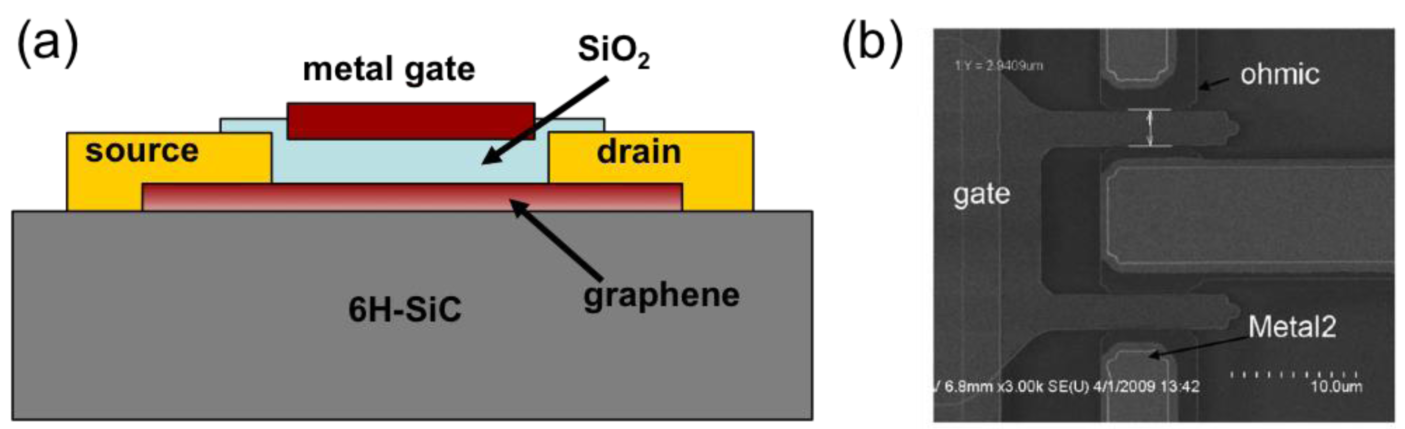
2. Experimental Section

Top-gated GFETs fabricated with epitaxial graphene layers grown on Si-face 6H-SiC substrates via Si sublimation were used in this study [10]. A schematic diagram of the top-gated GFET and a scanning electron microscope image of the test structure are shown in Figure 1a,b [10]. The top-gated GFETs were fabricated using Ti/Pt/Au source and drain contacts as well as Ti/Pt/Au metal gates over a 35 nm SiO2 dielectric layer deposited via electron beam evaporation [10,11]. Two-finger GFET structures with a 3 μm gate length (L) and various gate widths (W) were selected for total dose experiments. The test structures were exposed to Co-60 gamma rays at the Naval Research Laboratory (NRL) at a dose rate of ~910 rad(Si)/s with a positive gate bias of Vg = 3 V and all other terminals grounded. Electrical characterization was performed following step-stress irradiations up to a total dose of 1000 krad(Si). The characterization consisted of measuring the output characteristics (i.e., Id-Vds) by sweeping Vd from 0 to 3 V and stepping Vg from 2 V to −4 V in −1.0 V steps for Vs = 0, and the transfer characteristics (i.e., Id-Vgs) for Vd = 0.1 and 1 V for Vs = 0. For the transfer characteristics dual gate sweeps were done with Vg being swept from 2 V to −5 V then back to 2 V to observe the effects of gate hysteresis. In the top-gated GFET test structures used in this study, the graphene layer was not directly exposed to the experimental environment (i.e., it is covered by the SiO2/metal-gate stack; see Figure 1). Nevertheless, half of the samples were irradiated in air and the other half with a continuous flow of ultra pure N2 purging oxygen, moisture and other contaminants from the irradiation vessel. Both cases revealed negative shifts in the I-V characteristics but significant shifts in the minimum conductivity were only observed for devices tested in air. Additionally, gate hysteresis did not change significantly as a function of TID but consistent shifts in the negative and positive Vg sweeps were observed in the post-irradiation Id-Vgs characteristics of all devices. These shifts are due to radiation-induced positive oxide trapped charge and were analyzed independently of the mechanisms that cause hysteresis. The results are summarized and discussed in Section 3.
Figure 1. (a) Schematic diagram of top-gated graphene FET (GFET) fabricated with epitaxial graphene layers grown on Si-face 6H-SiC substrates via Si sublimation; (b) Scanning electron microscope (SEM) image of the GFET test structure.
Electronics 02 00234 g001

3. Results and Discussion

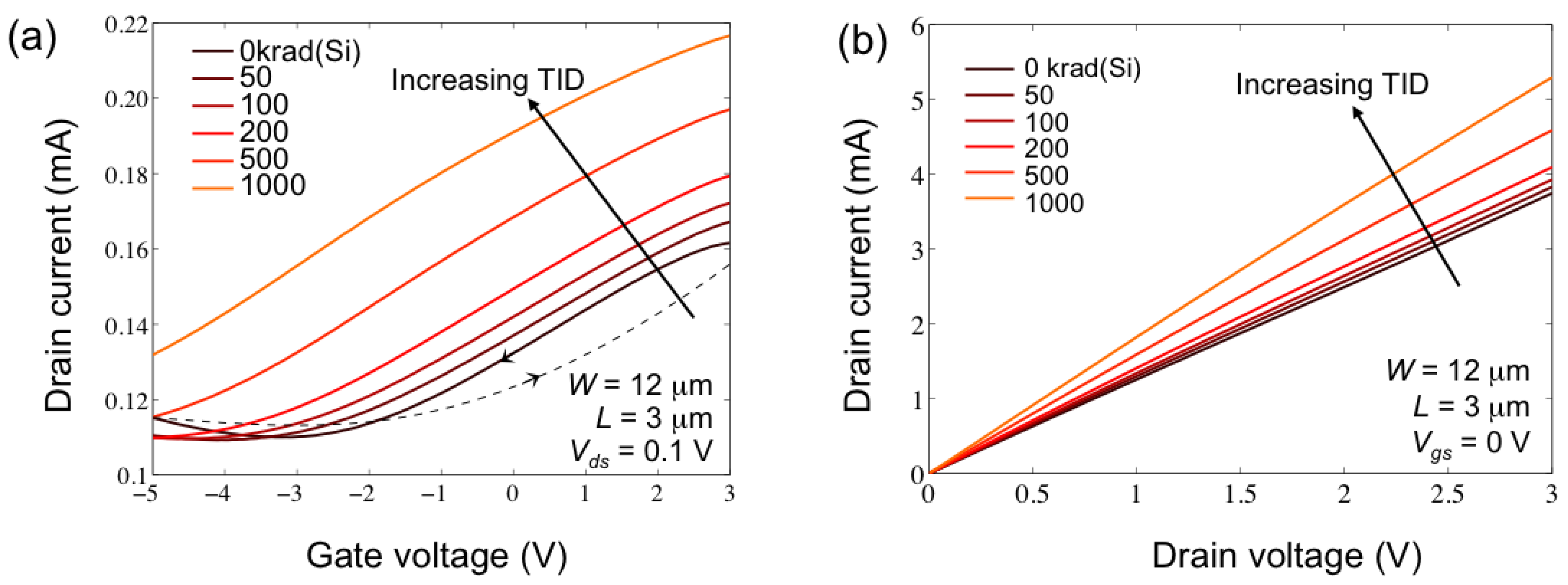
3.1. Current-Voltage Characteristics

Shown in Figure 2a are the Id-Vg characteristics for a two-finger GFET with W = 25 μm and L = 3 μm following step-stress irradiations in air up to 1000 krad(Si) and measured using Vds = 1 V. The measurements in Figure 2a reveal negative shifts in the I-V characteristics as well as an increase in the minimum drain current (Id-min) as a function of TID. These results indicate a buildup of Not near the SiO2/graphene layer interface shifting the minimum conductivity gate voltage (i.e., the Dirac voltage VDirac) negatively as well as increasing the minimum conductivity (σmin). The increased σmin results from increasing graphene channel intrinsic charge density (qint) as a function of dose (i.e., with time during the experiment). In Figure 2a the solid lines are Id measurements from positive to negative Vg sweeps and the dashed line are from negative to positive Vg sweep measurements as indicated by the arrows in the 0 krad(Si) curve. These are included to indicate hysteresis effects even prior to irradiation. Figure 2b is a plot of the extracted shifts in the Dirac point (i.e., ΔVDirac = VDiracVDirac0) and the relative increase in Id-min (i.e., Id-min/Id-min0) from the data in Figure 2a. VDirac0 and Id-min0 are respectively the Dirac voltage and Id at Vg = VDirac for 0 krad(Si) (i.e., prior to irradiation). The extractions in Figure 2b indicate a monotonic shift in VDirac and an increase in Id-min with total dose.
Figure 2. (a) Drain current (Id) plotted as a function of the gate voltage (Vg) for increasing total ionizing dose (TID) up to 1000 krad(Si), Vd = 1 V, Vs = 0 V. Measurements are for a two-finger GFET with W = 25 μm and L = 3 μm; (b) Extracted shifts in the Dirac voltage (ΔVDirac) and relative increase in Id-min plotted as a function of TID.
Electronics 02 00234 g002
Shown in Figure 3a are the Id-Vd characteristics for Vgs = 0 V, −1 V and −2 V measured at the same dose levels as show in Figure 2. The measurements in Figure 3 indicate an increase in Id as a function of total dose for all values of Vgs. The increase in Id is consistent with the negative shifts in Id-Vg characteristics (i.e., at a given Vg > VDirac, Id will increase as a function of dose for all values of Vd due to the negative voltage shift in the Id-Vg characteristics). Using the Id-Vd measurements for all Vg steps (i.e., from 2 V to −4 V), it is possible to represent Id-Vg curves for any Vds value contained within the sweep range of Vd (i.e., between 0 and 3 V). For example, shown in Figure 3b are representations of Id-Vgs for Vds = 0.1 V and for all dose levels. In Figure 3b symbols are data and solid lines are a least squares fits to the data. Figure 4 is a plot of ΔVDirac and Δσmin obtained from the data in Figure 3b. By comparison, the Id-Vg representations retain the TID effects observed in Figure 2.
Another TID effect, although not completely apparent from the measurements in Figure 2, Figure 3, is the degradation of carrier mobility. Degradation of carrier mobility is due to increased carrier scattering mechanisms that result from the buildup of oxide-trapped charges near the SiO2/graphene channel interface [5,12]. The increase in carrier scattering as a function of ionizing radiation is demonstrated in section 3.3 through calculations of effective electron mobility (μeff) based on extractions of drain conductance Electronics 02 00234 i002
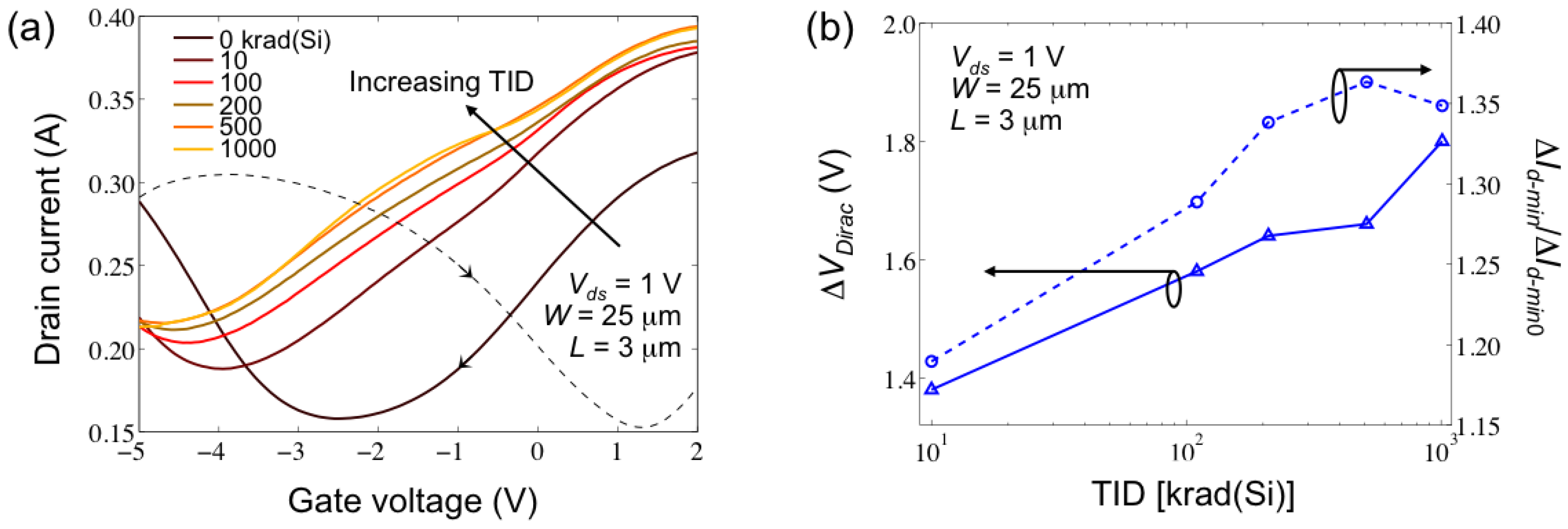
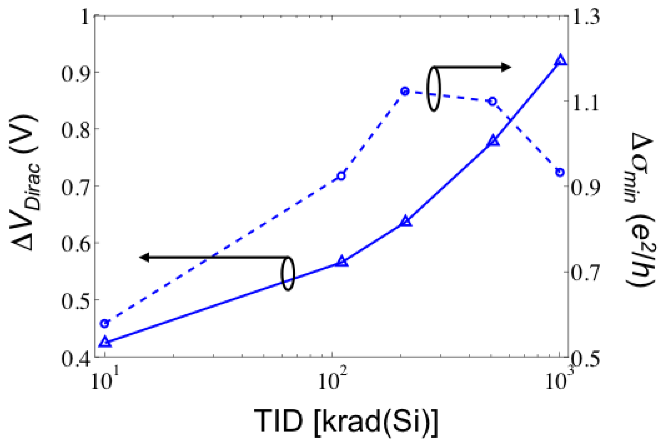
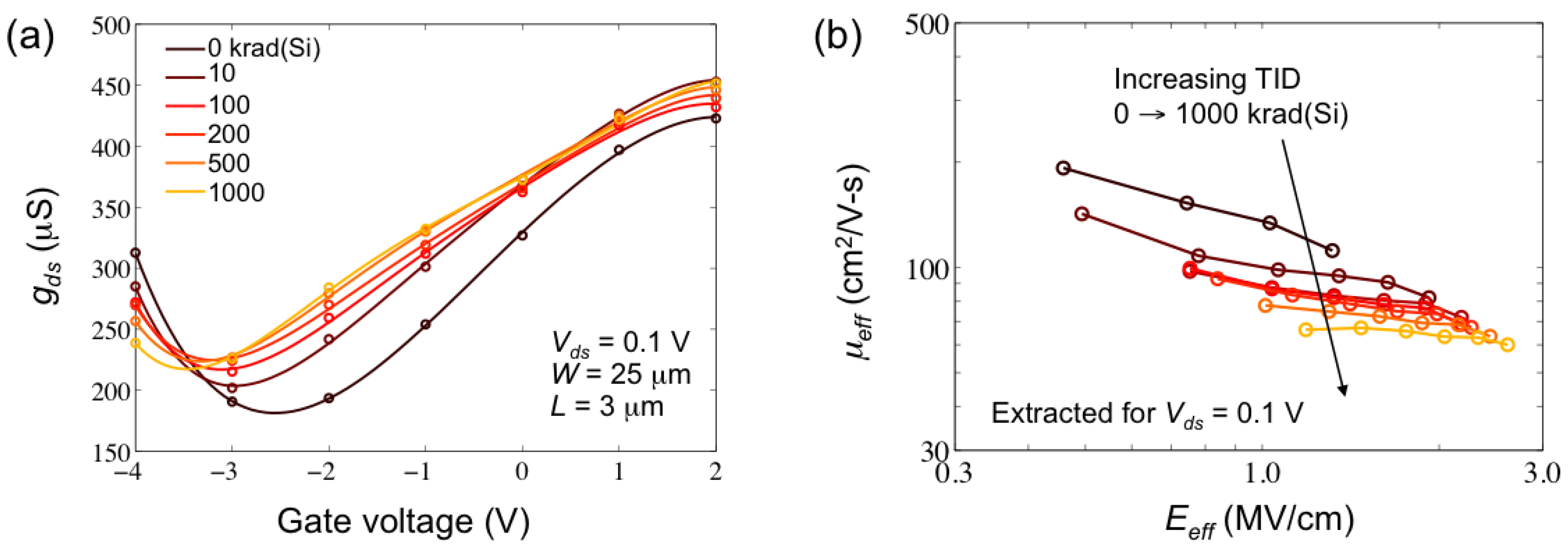
, ΔVDirac and Δσmin. Using ΔVDirac and Δσmin plotted in Figure 4 (extracted from the Id-Vg representations in Figure 3b) ensures that any contributions from hysteresis effects are equivalent for the extractions of gds since the same Id-Vds measurements are used for all of the extractions.
Figure 3. (a) Drain current (Id) plotted as a function of the drain voltage (Vd) for increasing TID up to 1000 krad(Si), Vg = 0, −1 and −2 V, Vs = 0 V. Measurements are for a two-finger graphene field effect transistors (GFET) with W = 25 μm and L = 3 μm; (b) Id-Vg representation for Vd = 0.1 V and for all dose levels. Symbols are data and solid lines are a least squares fits.
Electronics 02 00234 g003
Figure 4. Shifts in the Dirac voltage (ΔVDirac = VDiracVDirac0) and minimum conductivity (Δσmin = σminσmin0) obtained for Vds = 0.1 V in Figure 3b. Note: VDirac0 = −2.58 V, σmin0 = 4.7 e2/h (e = 1.6 ×10¹⁹ C, h = 6.63 ×10⁻³⁴ J-s).
Electronics 02 00234 g004

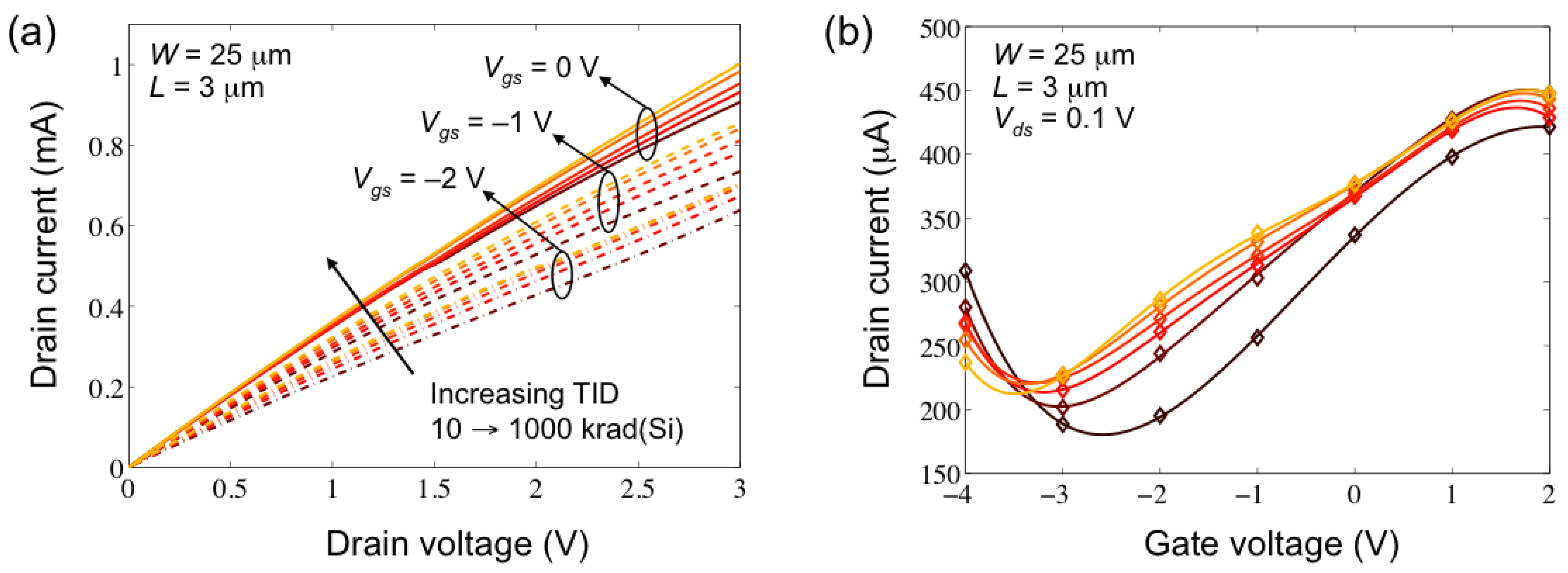
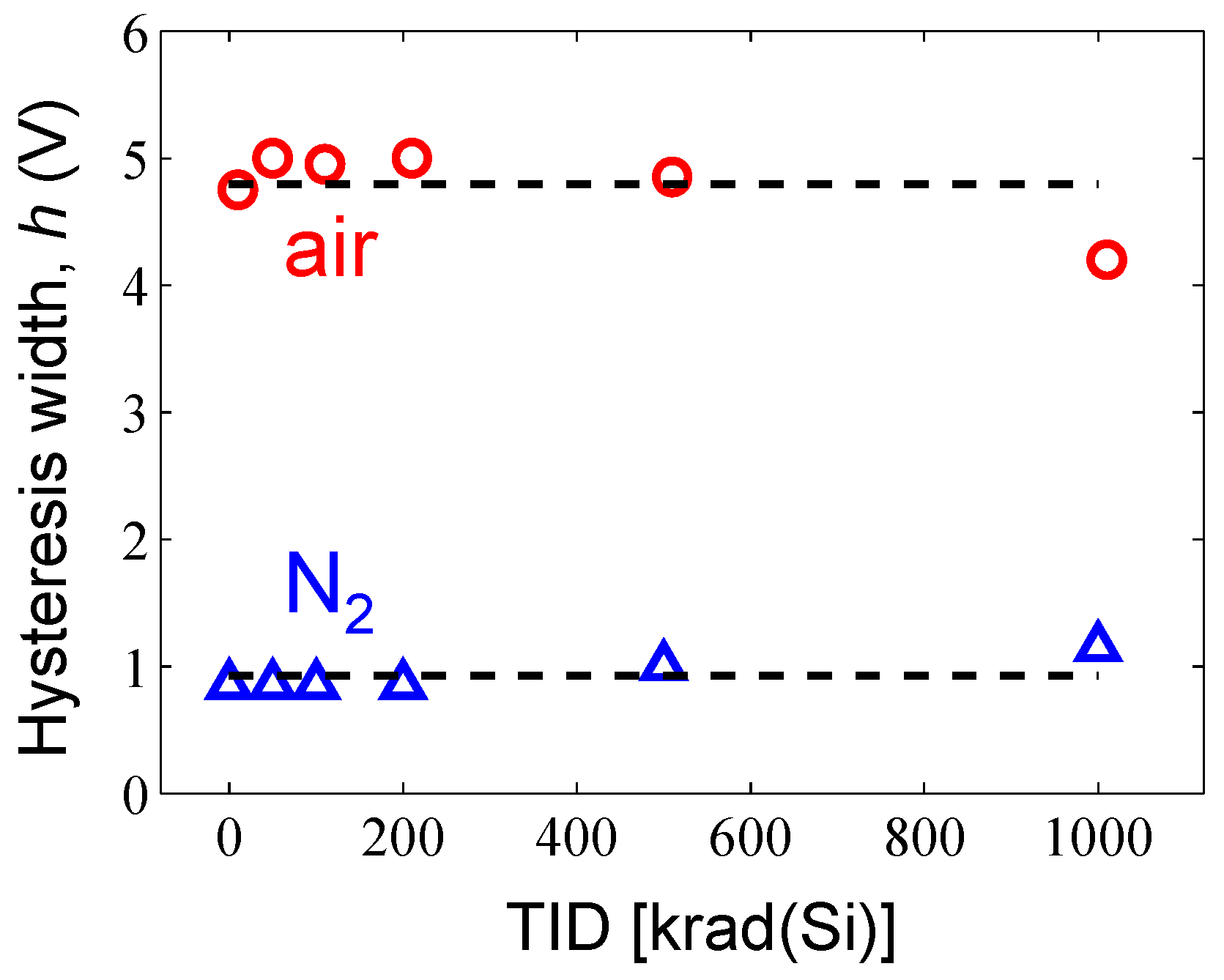
3.2. Experimental Ambient Conditions

Shown in Figure 5a,b are the Id-Vg and the Id-Vd characteristics for a GFET device with W = 12 μm and L = 3 μm irradiated with a continuous flow of ultra pure N2 purging the testing vessel. The response observed in Figure 5a,b reveals negative voltage shifts consistent with positive trapped charge as seen for devices irradiated in air. However, the devices irradiated with the N2 purge have less hysteresis and show negligible shifts in σmin. These differences indicate that molecular adsorption at the SiO2 surface near the graphene channel (resulting from moisture and contaminants in the experimental environment) does have an effect, albeit reduced, on the electrical characteristics of top-gated GFET test structures. Therefore, it is possible that any increase in σmin might be due to contaminants in the testing environment and not an effect of ionizing radiation exposure. In that case, the observed increase in σmin for devices tested in air might be the result from accumulated adsorption of contaminants in the testing environment. For devices exposed with flowing N2, the concentration of the contaminants was significantly reduced and therefore σmin did not change significantly. Figure 6 plots extractions of hysteresis width (h) as a function of TID for both devices irradiated in air and with flowing N2. Hysteresis width is extracted as the difference in the Vg intercept at a constant current for the negative and positive sweeps. The extractions of h reveal larger widths for devices tested in air, as expected due molecular adsorption at the surface of the SiO2 contributing to charge trapping mechanisms that cause hysteresis [13]. However both experiments show negligible changes in hysteresis with TID. The radiation-induced degradation of effective carrier mobility is analyzed independently of the mechanisms that cause hysteresis in Section 3.3 based on these observations.
Figure 5. (a) Drain current (Id) plotted as a function of the gate voltage (Vg) for increasing TID up to 1000 krad(Si), Vd = 1 V, Vs = 0 V. Measurements are for a two-finger GFET with W = 12 μm and L = 3 μm; (b) Drain current (Id) plotted as a function of the drain voltage (Vd) for Vs = 0 V and for increasing TID up to 1000 krad(Si).
Electronics 02 00234 g005
Figure 6. Extraction of hysteresis width (h) as a function of TID for devices tested in air and with flowing N2 purge. Symbols are data and dashed line is the mean hysteresis width.
Electronics 02 00234 g006

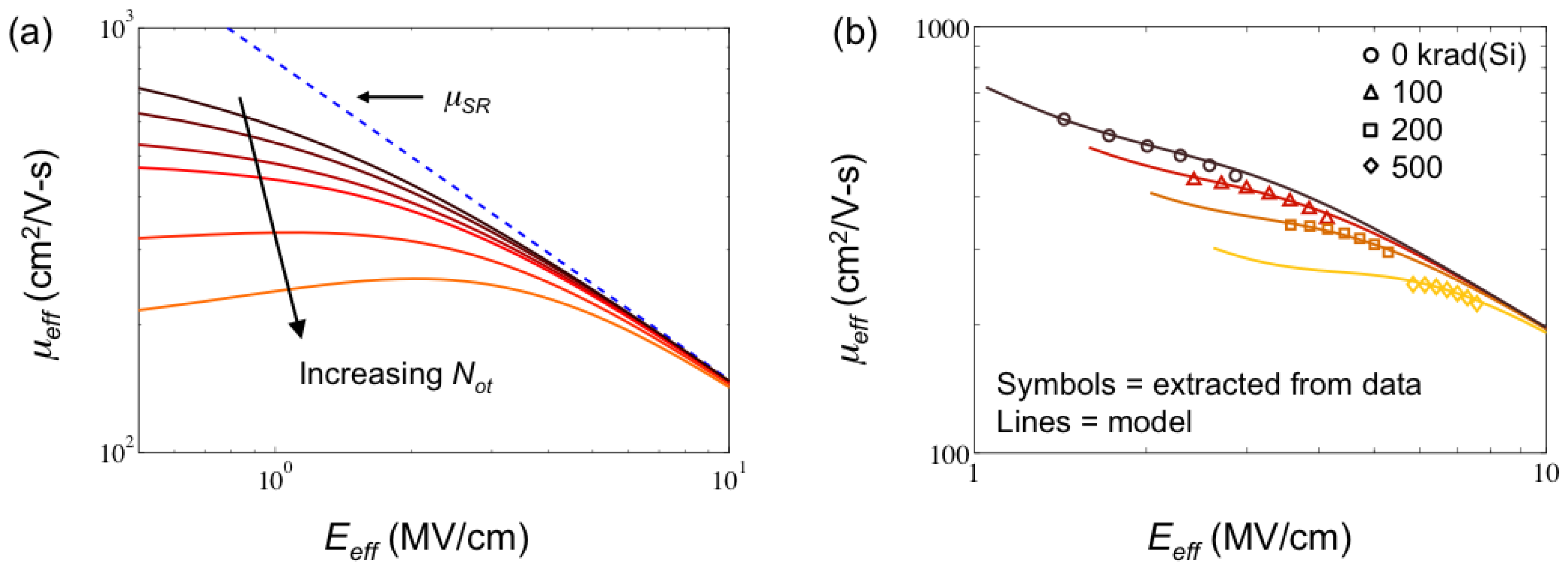
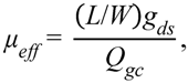
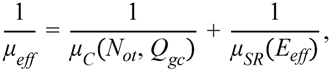
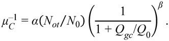
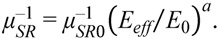
3.3. Mobility Degradation

The radiation-induced degradation of carrier mobility is determined through calculations of effective electron mobility in the graphene layer (μeff) as a function of the effective vertical field (Eeff). The effective electron mobility is given by
Electronics 02 00234 i003
where Qgc is the graphene channel charge density [14]. The effective vertical field in the graphene channel is estimated as [10]
Electronics 02 00234 i004
and the graphene channel charge density is calculated as
Electronics 02 00234 i005
Here, qint is the graphene channel intrinsic charge density that results from charge inhomogeneity in the graphene layer typically described as electron-hole puddles that arise from the random charged impurity potential fluctuations and contribute to the non-zero minimum conductivity at the Dirac point [15,16,17,18].
Shown in Figure 7a is gds plotted as a function of Vg for all dose levels. Calculations of μeff using Equations 1–3 are plotted in Figure 7b as a function of Eeff and for increasing TID. In the calculations, qint is estimated by σmin/μFE, μFE is the peak field effect mobility and gds is extracted for Vds = 0.1 V. The results in Figure 7b reveal a decrease in μeff with increasing total dose as can be observed at Eeff ~ 1 MV/cm. Deviations from the pre-irradiation μeff(Eeff) characteristics are due to the increased contribution of scattering mechanisms that results from radiation-induced oxide trapped charges. The deviations from the pre-irradiation μeff(Eeff) curve are expected to continue towards lower values of Eeff (i.e., towards lower carrier densities nEeff) where scattering due to charged impurities is the dominant mechanism. Other scattering mechanisms such as short-range scattering dominate for large carrier densities (n) [15,19] (i.e., for large Eeff) and the μeff(Eeff) characteristics converge to a universal response. In Figure 7b this convergence appears for Eeff > 2 MV/cm.
In the approach presented here, the calculations of Qgc (and Eeff) capture the contribution of radiation-induced oxide trapped charges through the shifts in VDirac. Therefore, this approach allows determining the radiation-induced degradation of carrier mobility in GFET devices without ambiguities introduced by voltage shifts in the Id-Vg characteristics and the changes in σmin. These ambiguities exist, for example, when plotting μFE as a function of Vg at various levels of TID. Nonetheless, it should be noted that discrepancies in the calculations of μeff could result from the approximations made in Equations 1–3. Interface states have not been included in the extractions presented here, but can be incorporated by including an interface trap charge density (bias-dependent) term Qit(Vg, Nit) in Equation 3. Additionally, non-uniform buildup of Not may result from non-uniform field distributions in the gate oxide (e.g., in regions not covered by the top gate). These conditions would require a more sophisticated calculation of Qgc, but the basic methodology presented here would still apply. The following section describes a semi-empirical modeling approach for the degradation of effective carrier mobility based on the experimental observations of μeff(Eeff) and its response to ionizing radiation.
Figure 7. (a) Drain conductance (gds) plotted as a function of the gate voltage at Vd = 0.1 V for increasing dose levels up to 1000 krad(Si); (b) Effective electron mobility (μeff) plotted as a function of the effective vertical field (Eeff) for increasing total dose levels up to 1000 krad(Si).
Electronics 02 00234 g007

4. Modeling

This section presents a semi-empirical modeling approach for describing effective carrier mobility in GFET devices and its degradation due ionizing radiation exposure. The radiation-induced shifts in VDirac can be directly related to Not as
ΔVDirac = −qΔNot/Cox.
In (4), Not accounts for the buildup of radiation-induced trapped charges that image charge into the graphene layer, Cox is the oxide capacitance per unit area and q is the electronic charge. The effective electron carrier mobility is expressed using Matthiessen’s rule as
Electronics 02 00234 i007
where Eeff is calculated using Equations 2 and 3 and VDirac as given by Equation 4 (i.e., VDirac = VDirac0qΔNot/Cox). In Equation 5, μC is the Coulomb scattering limited effective carrier mobility and is modeled as a function of Not and Qgc as
Electronics 02 00234 i008
In Equation 5, μSR corresponds to the short-range scattering that dominates for large n and is given by
Electronics 02 00234 i009
Equations 6 and 7 are adapted from a semi-empirical model for inversion layer mobility in Si MOSFETs described in [20]. Figure 8a shows calculations of μeff using Equations 5–7 and plotted as a function of Eeff for increasing Not. For the calculations in Figure 8a, α = 0.005 V-s/cm2, μSR0 = 1000 cm2/V-s, β = 2, a = 0.75, N0 = 1012 cm−2, Q0 = 10−6 C/cm2, E0 = 106 V/cm, Eeff is in units of V/cm, Qgc in units of C/cm2 and Not is in units of cm−2. The calculations in Figure 8a correctly describe the reduction in μeff with Not (i.e., μeff ∝ 1/Not) for low n and the merging with μSR (dashed lined) for large n. In the model, parameters a, μSR0, α and β can be treated as fitting parameters and Q0, E0 and N0 are constants that allow a simpler interpretation of the units for Eeff, Qgc and Not.
An increase in μeff for decreasing Eeff < ~1 MV/cm can be modeled empirically adding μ0 = A(E0/Eeff)b to the calculation of μeff given by Equation 5. This allows obtaining good agreements with the experimental results. This increase in mobility for decreasing n has been reported in [19] and attributed to scatterer transparency occurring when carrier wavelengths exceed the spacing between scatterers. In this work, the μeff dependence to scatterer transparency in the low n limit is modeled independently from charged impurity and short-range scattering using the aforementioned empirical form. Shown in Figure 8b are calculations of μeff compared with extractions from experimental data from irradiated GFETs. For the calculations in Figure 8b the fitting parameters are α = 0.08 V-s/cm2, μSR0 = 2000 cm2/V-s, A = 340 cm2/V-s, β = 4, a = 0.85, b = 1.08, N0 = 1012 cm−2, Q0 = 10−6 C/cm2 and E0 = 106 V/cm. As shown in Figure 8b, the model calculations fit the experimental data with good qualitative agreement validating the presented approach. Additional experimental observations of scatterer transparency and the merging of μeff(Eeff) at large n for short range limited scattering would further validate the modeling of radiation-induced degradation as an independent mechanism utilizing Matthiessen’s rule. Nevertheless, the modeling approach presented here can be directly applied to calculations described in [21,22,23] for model radiation-induced degradation in GFET I-V characteristics.
Figure 8. (a) Calculations of the effective electron mobility (μeff) using Equations 5–7 and plotted as a function of the effective vertical field (Eeff) for increasing values of Not. The dashed line corresponds to the short-range mobility given by Equation 7; (b) Comparison of μeff extracted from data in Figure 5 (symbols) and model calculations (lines) including scatterer transparency.
Electronics 02 00234 g008

5. Conclusions

In this work, we have investigated TID effects in top-gated epitaxial GFETs. Oxide charge trapping near the SiO2/graphene channel interface has been identified as the main contributing mechanisms to radiation-induced degradation. The effects of the radiation-induced oxide trapped charges are manifested as negative voltage shifts in the I-V characteristics and carrier mobility degradation. These effects have been observed for devices exposed in air as well as for devices exposed with flowing ultra pure N2 purging moisture contaminants from the irradiation vessel. Extractions of shifts in the Dirac voltage (ΔVDirac) indicate buildup of oxide trapped charge densities (ΔNot) of ~ 1012 cm−2 at dose levels of 1000 krad(Si). The experimental results also reveal a significant increase in minimum conductivity (σmin) for devices tested in air. Since σmin was initially low in these samples (i.e., σmin0 = 4.7 e2/h) the increase may be due to compensation and/or reorganization of the potential fluctuations in the graphene layer as a result of molecular adsorption at the SiO2 surface near the graphene channel [5].
The results reported in this work confirm that GFET devices with top-gated structures are also susceptible to TID effects that result from the buildup of oxide-trapped charges. Mitigation of these degradation mechanisms is required for the successful implementation of GFET devices in space-based applications. An example of such a mitigation technique based on local etching of the dielectric layer in the active regions of back-gated GFETs is described in [5]. However, GFET devices with independent top-gates are desirable for the fabrication of integrated circuits. The devices used in this work were research test structures with relatively thick gate dielectrics. Alternative mitigation approaches such as the using thin top-gate dielectric layers may be available soon as advances in the processing of graphene devices allows further scaling.
An approach for extracting the radiation-induced degradation of the effective carrier mobility from the degraded I-V characteristics of irradiated GFETs is presented in this paper. This approach accounts for shifts in VDirac as well as changes in the minimum conductivity by introducing an intrinsic charge density component (i.e., qint) into the calculations of the total graphene layer charge (i.e., Qgc). The extractions of effective electron mobility (μeff) indicate deviations from the pre-irradiation μeff(Eeff) dependence that are due to the increased contribution of scattering mechanisms resulting from oxide-trapped charges. For large values of effective vertical field (Eeff) the extractions merge at the pre-irradiation curve as mechanisms other than charged impurity scattering become dominant for large carrier densities (i.e., nEeff). Similar results were observed recently for Cu-CVD back-gated GFETs irradiated with Co-60 gamma rays [24]. Additionally, an increase in μeff is observed for Eeff < 1 MV/cm that is consistent with the observations made in [19] and attributed to scatterer transparency that occurs as carrier wavelengths becomes larger than scatterer spacing. The presented approach can be extended to incorporate interface traps, non-uniform buildup of Not and the effects of contact resistance as needed based on further experimental investigation.
Additionally, this work introduces a semi-empirical approach for modeling radiation-induced degradation of μeff based on calculations of Eeff and Qgc that incorporate the buildup of Not. The degradation of μeff due to charge impurity scattering is modeled as an independent scattering mechanism according to Matthiessen’s rule. The appearance of scatterer transparency is modeled empirically as a function of Eeff resulting in good qualitative agreement with the experimental extractions of μeff and its radiation response.

Acknowledgments

This work was supported (in part) by the Defense Threat Reduction Agency, Basic Research Award # HDTRA1-10-1-0015, to the USC Information Sciences Institute and the University of Southern California.

Conflict of Interest

The authors declare no conflict of interest.

References

  1. Geim, K.; Novoselov, K.S. The rise of graphene. Nat. Mater. 2007, 6, 183–191. [Google Scholar] [CrossRef]
  2. Schwierz, F. Graphene transistors. Nat. Nanotechnol. 2010, 5, 487–496. [Google Scholar] [CrossRef]
  3. Meric, I.; Han, M.Y.; Young, A.F.; Ozyilmaz, B.; Kim, P.; Shepard, K.L. Current saturation in zero-bandgap, top-gated graphene field-effect transitors. Nat. Nanotechnol. 2008, 3, 654–659. [Google Scholar] [CrossRef]
  4. Zhang, E.X.; Newaz, A.K.; Wang, B.; Bhandaru, S.; Zhang, C.X.; Fleetwood, D.M.; Bolotin, K.I.; Pantelides, S.T.; Alles, M.L.; Schrimpf, R.D.; et al. Low-energy X-ray and ozone-exposure induced defect formation in graphene materials and devices. IEEE Trans. Nucl. Sci. 2011, 58, 2961–2967. [Google Scholar] [CrossRef]
  5. Cress, C.D.; McMorrow, J.J.; Robinson, J.T.; Landi, B.J.; Hubbard, S.M.; Messenger, S.R. Radiation effects in carbon nanoelectronics. Electronics 2012, 1, 23–31. [Google Scholar] [CrossRef]
  6. Mai-Xing, H.; Zhuo-Yu, J.; Li-Wei, S.; Ying-Ping, C.; Hong, W.; Xin, L.; Dong-Mei, L.; Ming, L. Gamma radiation caused graphene defects and increased carrier density. Chin. Phys. B 2011, 20, 086102. [Google Scholar] [CrossRef]
  7. Zhang, C.X.; Zhang, E.X.; Fleetwood, D.M.; Alles, M.L.; Schrimpf, R.D.; Song, E.B.; Sung, M.K.; Galatsis, K.; Wang, K.L.W. Electrical stress and total ionizing dose effects on graphene-based non-volatile memory devices. IEEE Trans. Nucl. Sci. 2012, 59, 2974–2978. [Google Scholar] [CrossRef]
  8. Cress, C.; McMorrow, J.; Robinson, J.; Friedman, A.; Landi, B. Radiation effects in single-walled carbon nanotube thin-film-transistors. IEEE Trans. Nucl. Sci. 2010, 57, 3040–3045. [Google Scholar]
  9. Fu, Y.; Zhang, J.; Wang, C.; Zhou, C.; Wormuth, R.; Tyree, V.; Fritze, M.; McMarr, P.; Hughes, H. Total Dose Radiation Effects in Carbon Nanotube Transistors. In Presented at the Government Microcircuit Applications and Critical Technology Conference, Las Vegas, NV, USA, March 2012.
  10. Moon, J.S.; Curtis, D.; Bui, S.; Hu, M.; Gaskill, D.K.; Tedesco, J.L.; Asbeck, P.; Jernigan, G.G.; VanMil, B.L.; Myers-Ward, R.L.; et al. Top-gated epitaxial graphene FETs on Si-Face SiC Wafers With a peak transconductance of 600 mS/mm. IEEE Electron Dev. Lett. 2010, 31, 260–262. [Google Scholar] [CrossRef]
  11. Russo, S.; Craciun, M.F.; Yamamoto, M.; Tarucha, S.; Morpurgo, A.F. Double-gated graphene-based devices. New J. Phys. 2009, 11, 095018. [Google Scholar] [CrossRef]
  12. Chen, J.-H.; Jang, C.; Adam, S.; Fuhrer, M.S.; Williams, E.D.; Ishigami, M. Charge impurity scattering in graphene. Nat. Phys. 2008, 4, 377–381. [Google Scholar] [CrossRef]
  13. Kim, W.; Javey, A.; Vermesh, O.; Wang, Q.; Li, Y.; Dai, H. Hysteresis caused by water molecules in carbon nanotube field-effect transistors. Nano Lett. 2003, 3, 193–198. [Google Scholar] [CrossRef]
  14. Sun, S.C.; Plummer, J.D. Electron mobility in inversion and accumulation layers on thermally oxidized silicon surfaces. IEEE J. Solid-State Circ. 1980, 27, 1497–1508. [Google Scholar]
  15. Wehling, T.O.; Şaşıoğlu, E.; Friedrich, C.; Lichtenstein, A.I.; Katsnelson, M.I.; Blügel, S. Strength of effective coulomb interactions in graphene and graphite. Phys. Rev. Lett. 2011, 106, 236805. [Google Scholar]
  16. Martin, J.; Akerman, N.; Ulbricht, G.; Lohmann, T.; Smet, J.H.; von Klitzing, K.; Yacoby, A. Observation of electron-hole puddles in graphene using a scanning single-electron transistor. Nat. Phys. 2008, 4, 144–148. [Google Scholar] [CrossRef]
  17. Chen, J.-H.; Cullen, W.G.; Jang, C.; Fuhrer, M.S.; Williams, E.D. Defect scattering in graphene. Phys. Rev. Lett. 2009, 102, 236805. [Google Scholar] [CrossRef]
  18. Adam, S.; Hwang, E.H.; Galitski, V.M.; Sarma, S.D. A self-consistent theory for graphene transport. Proc. Natl. Acad. Sci. USA 2007, 104, 18392–18397. [Google Scholar]
  19. Farmer, D.B.; Perebeinos, V.; Ling, Y.; Dimitrakopoulos, C.; Avouris, P. Charge trapping and scattering in epitaxial graphene. Phys. Rev. B 2011, 84, 205417. [Google Scholar] [CrossRef]
  20. Cheng, B.; Woo, J. Measurement and modeling of the n-channel and p-channel MOSFET’s inversion layer mobility at room and low temperature operation. J. Phys. IV France 1996, 6, 43–47. [Google Scholar]
  21. Thiele, S.A.; Schaefer, J.A.; Schwierz, F. Modeling of graphene metal-oxide-semiconductor field-effect transistors with gapless large-area graphene channels. J. Appl. Phys. 2010, 107, 094505. [Google Scholar] [CrossRef]
  22. Meric, I.; Baklitskaya, N.; Kim, P.; Shepard, K.L. RF Performance of Top-Gated, Zero-Bandgap Graphene Field-Effect Transistors. In Proceedings of Electron Devices Meeting, San Francisco, CA, USA, December 2008; pp. 1–4.
  23. Champlain, J.G. A first principles theoretical examination of graphene-based field effect transistors. J. Appl. Phys. 2011, 109, 084515. [Google Scholar] [CrossRef]
  24. Cress, C.D.; Champlain, J.G.; Esqueda, I.S.; Robinson, J.T.; Friedman, A.L.; McMorrow, J. Total ionizing dose induced charge carrier scattering in graphene devices. IEEE Trans. Nucl. Sci. 2012, 59, 3045–3053. [Google Scholar] [CrossRef]

