Carbon Nanotubes and Graphene Nanoribbons: Potentials for Nanoscale Electrical Interconnects

Abstract
:
1. Introduction
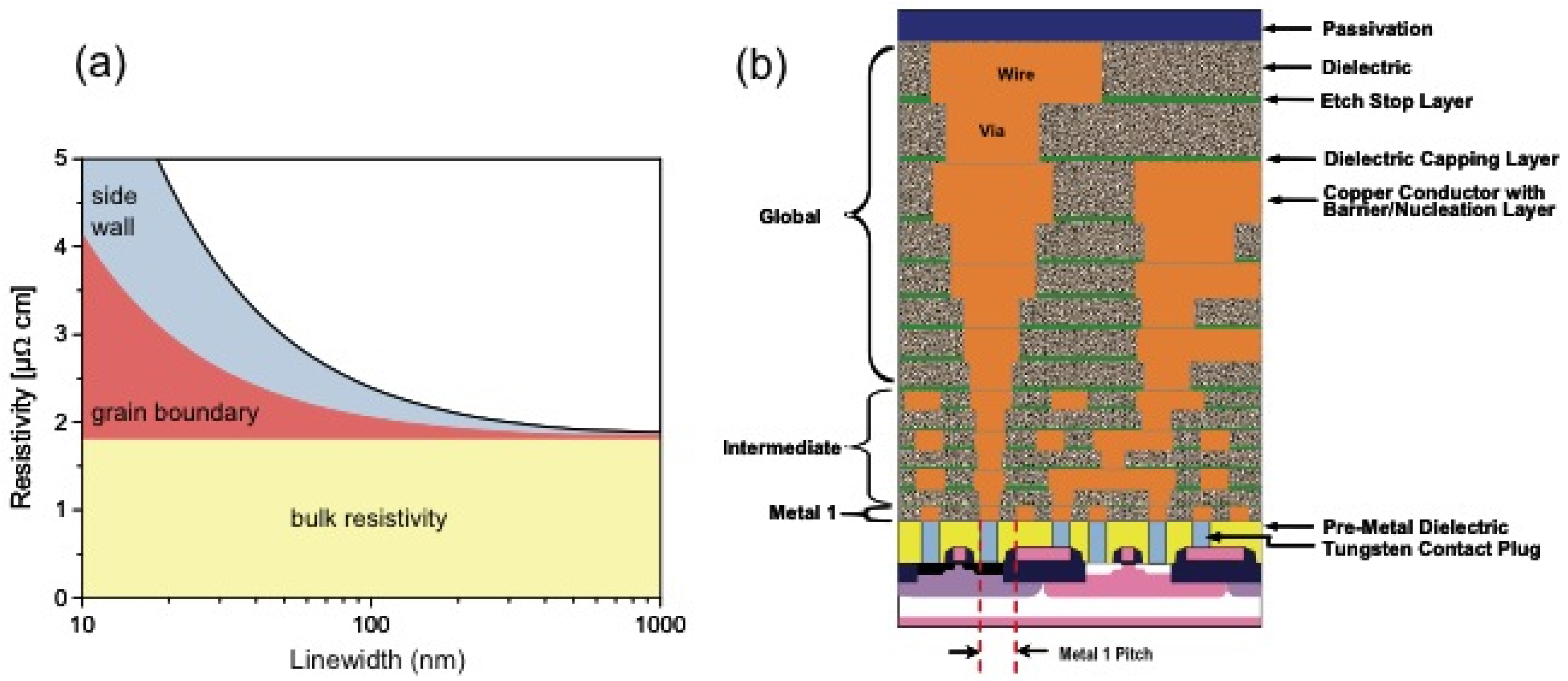
2. Carbon Nanotubes
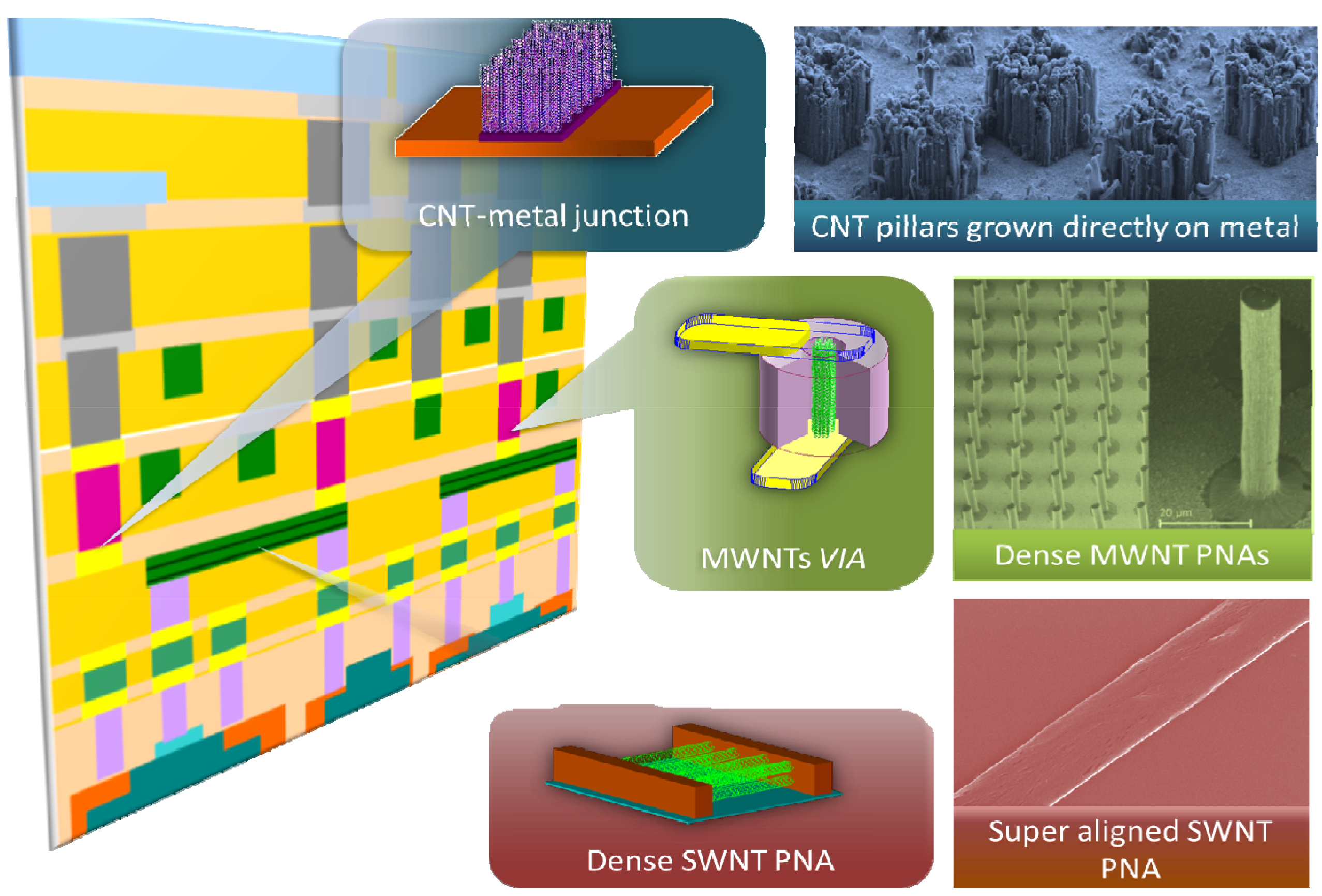
2.1. Carbon Nanotubes for High-Density Integration
2.1.1. Scalable Ultra-High Density, Super Aligned SWNT PNAs
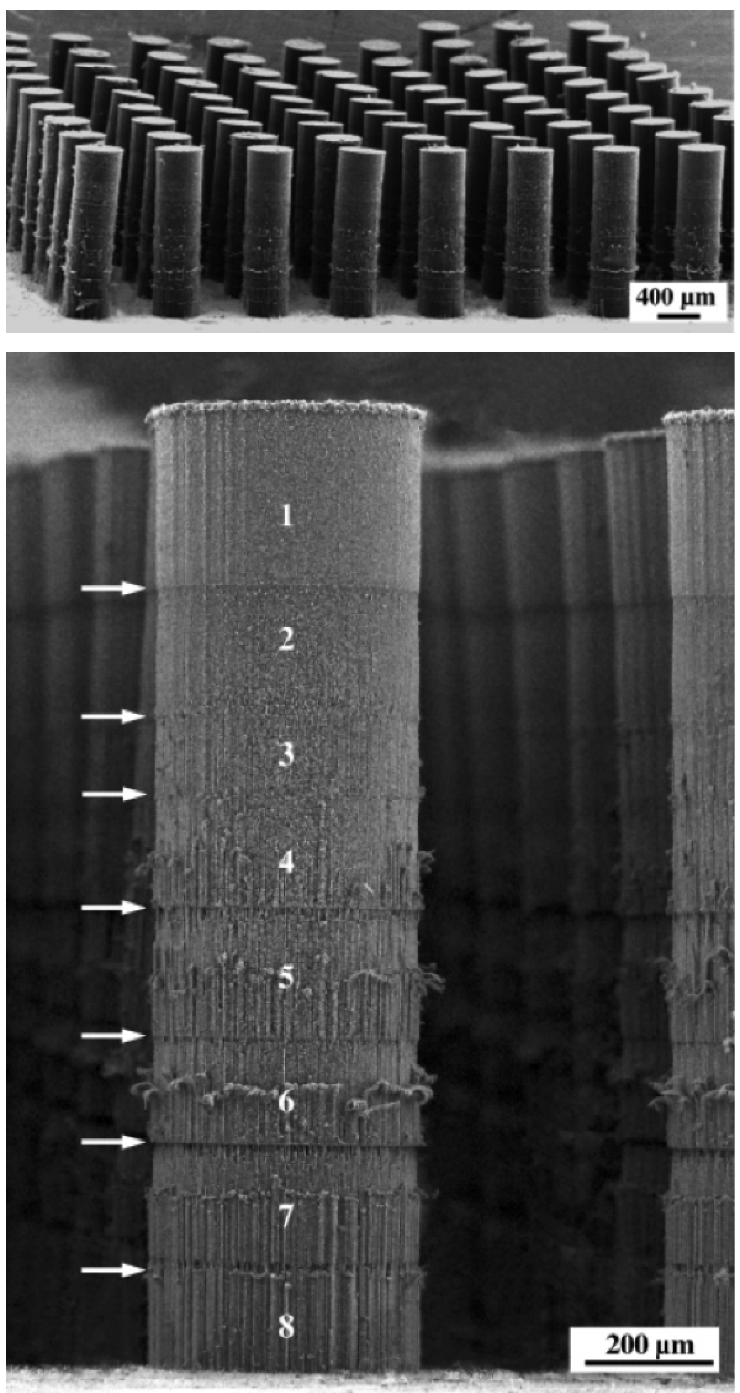
2.1.2. Densely Packed Ultra-Long MWNTs

2.1.3. Selective Growth of Metallic Tubes

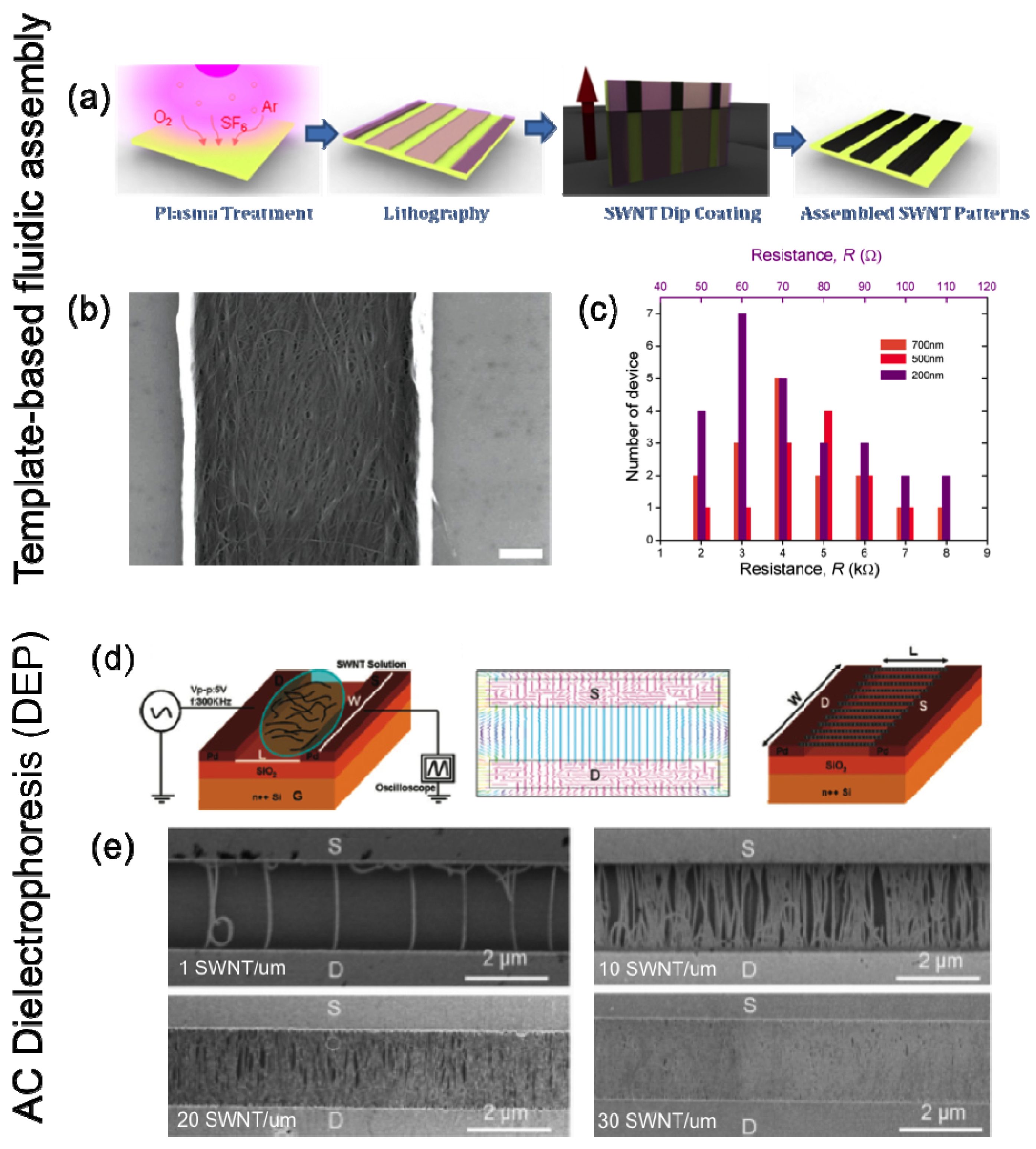
2.1.4. Directional Growth of CNTs
2.2. Carbon Nanotubes Devices and Architectures
2.2.1. Towards Low-Resistance Contacts

2.2.2. Towards Defect-Free CNTS
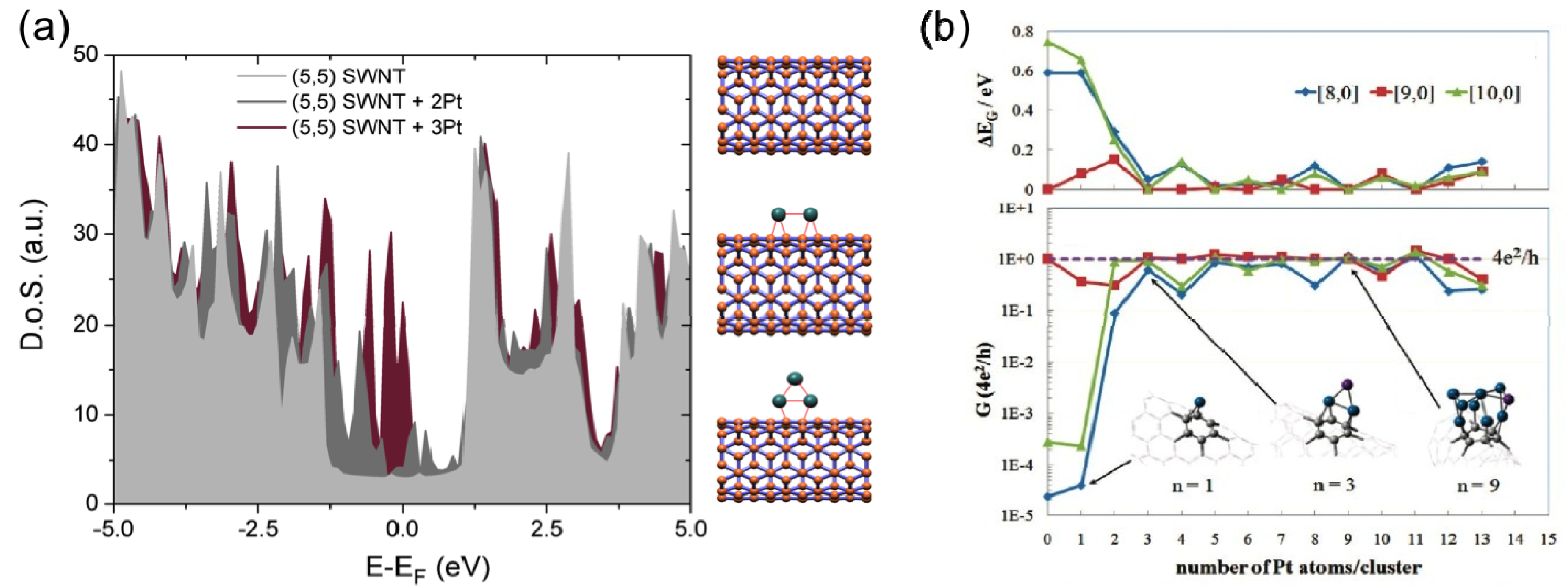
2.2.3. Conductance Enhancement via Metal Decoration and Doping
2.2.4. Breakdown in Carbon Nanotubes

3. Graphene and Graphene Nanoribbons
3.1. Graphene as Two-Dimensional Crystal
3.2. Graphene and Few-Graphene Layers Nanoribbons
- (i)
- Graphite-like NRs in place for lower interconnect resistance, especially for short interconnects. In the case of multiple layers, is indeed necessary that the layers in within the stack are yelectronically decoupled [81,120,172], condition which preserves graphene properties [173]. Further, in this case, all layers need to be electrically contacted.
- (ii)
- Few-layer GNR interconnects suitable in order to reduce the interconnect capacitance (~ as much as 50%), delay and power dissipation of local interconnects. This arrangement is particularly interesting for short local interconnects in which the delay is dominated by capacitive loading and not resistivity.
4. Conclusions and Future Challenges
Acknowledgements
Conflicts of Interest
References
- International Technology Roadmap for Semiconductors. Interconnect Chapter; SEMATECH: Austin, TX, USA, 2009, 2009 ed. Available online: http://www.itrs.net/Links/2009ITRS/2009Chapters_2009Tables/2009_Interconnect.pdf.
- Wu, W.; Brongersma, S.H.; van Hove, M.; Maex, K. Influence of surface and grain-boundary scattering on the resistivity of copper in reduced dimensions. Appl. Phys. Lett. 2004, 8, 2838–1. [Google Scholar]
- International Technology Roadmap for Semiconductors. Interconnect Chapter; SEMATECH: Austin, TX, USA, 2007, 2007 ed. Available online: http://www.itrs.net/Links/2007ITRS/2007_Chapters/2007_Interconnect.pdf.
- International Technology Roadmap for Semiconductors, 1999 ed.; In Interconnect ChapterSEMATECH: Austin, TX, USA, 1999.
- International Technology Roadmap for Semiconductors. Interconnect Chapter; SEMATECH: Austin, TX, USA, 2011, 2011 ed. Available online: http://www.itrs.net/Links/2011ITRS/2011Chapters/2011Interconnect.pdf.
- Miller, A.B. Optical interconnects to silicon. IEEE J. Sel. Top. Quantum Electron. 2000, 6, 1312–1317. [Google Scholar] [CrossRef]
- Lu, D. Recent advances on chip-to-chip optical interconnects. Proc. SPIE 2009. [Google Scholar] [CrossRef]
- Fischbach, R.; Lienig, J.; Meister, T. From 3D Circuit Technologies and Data Structures to Interconnect Prediction. In Proceeding of the 11th International Workshop on System Level Interconnect Prediction, San Francisco, CA, USA, 26–27 July 2009; pp. 77–84.
- Wei, B.Q.; Vajtai, R.; Ajayan, P.M. Reliability and current carrying capacity of carbon nanotubes. Appl. Phys. Lett. 2001, 79, 1172–1174. [Google Scholar] [CrossRef]
- Charlier, J.-C.; Blase, X.; Roche, S. Electronic and transport properties of nanotubes. Rev. Mod. Phys. 2007, 79, 677–732. [Google Scholar] [CrossRef]
- Javey, A.; Guo, J.; Wang, Q.; Lundstrom, M.; Dai, H. Ballistic carbon nanotube field-effect transistors. Nature 2003, 424, 654–657. [Google Scholar] [CrossRef]
- Berber, S.; Kwon, Y.-K.; Tománek, D. Unusually high thermal conductivity of carbon nanotubes. Phys. Rev. Lett. 2000, 84, 4613–4616. [Google Scholar] [CrossRef]
- Choi, T.-Y.; Poulikakos, D.; Tharian, J.; Sennhauser, U. Measurement of the thermal conductivity of individual carbon nanotubes by the four-point three-method. Nano Lett. 2006, 6, 1589–1593. [Google Scholar] [CrossRef]
- Close, G.F.; Yasuda, S.; Paul, B.; Fujita, S.; Wong, P.H.S. A 1 GHz integrated circuit with carbon nanotube interconnects and silicon transistors. Nano Lett. 2008, 8, 706–709. [Google Scholar] [CrossRef]
- Chaste, J.; Lechner, L.; Morfin, P.; Fève, G.; Kontos, T.; Berroir, J.-M.; Glattli, D.C.; Happy, H.; Hakonen, P.; Plaçais, B. Single carbon nanotube transistor at GHz frequency. Nano Lett. 2008, 8, 525–528. [Google Scholar] [CrossRef]
- Xu, Y.; Srivastava, A. A model for carbon nanotube interconnects. Int. J. Circuit Theory Appl. 2009, 38, 559–575. [Google Scholar]
- Srivastava, A.; Xu, Y.; Sharma, A.K. Carbon nanotubes for next generation very large scale integration interconnects. J. Nanophotonics 2010, 4, 041690:1–041690:27. [Google Scholar]
- Frank, S.; Poncharal, P.; Wang, Z.L.; de Heer, W.A. Carbon nanotube quantum. Resist. Sci. 1998, 280, 1744–1746. [Google Scholar]
- Van der Straten, O.; Zhy, Y.; Eisenbraun, E.; Kaloyeros, A. Thermal and Electrical Barrier Performance Testing of Ultrathin Atomic Layer Deposition Tantalum-Based Materials for Nanoscale Copper Metallization. In Proceedings of the IEEE International Interconnect Technology Conference, Burlingame, CA, USA, 5 June 2002; pp. 188–190.
- Watanabe, T.; Nasu, H.; Minamihaba, G.; Kurashima, N.; Gawase, A.; Shimada, M.; Yoshimizu, Y.; Uozumi, Y.; Shibata, H. Self-Formed Barrier Technology using CuMn Alloy Seed for Cu Dual-Damascene Interconnect with Porous-SiOC/ Porous-Par Hybrid Dielectric. In Proceedings of the IEEE International Interconnect Technology Conference, Burlingame, CA, USA, 4–6 June 2007; pp. 7–9.
- Zhou, Y.; Sreekala, S.; Ajayan, P.M.; Nayak, S.K. Resistance of copper nanowires and comparison with carbon nanotube bundles for interconnect applications using first principles calculations. J. Phys. Condens. Matter 2008, 20, 095209:1–095209:9. [Google Scholar]
- Maffucci, A.; Miano, G.; Villone, F. Performance comparison between metallic carbon nanotube and copper nano-interconnects. IEEE Trans. Adv. Packag. 2008, 31, 692–699. [Google Scholar] [CrossRef]
- Cho, H.; Koo, K.-H.; Kapur, P.; Saraswat, K.C. Performance comparisons between Cu/low-κ, carbon-nanotube, and optics for future on-chip interconnects. IEEE Electron Device Lett. 2008, 29, 122–124. [Google Scholar] [CrossRef]
- Naeemi, A.; Meindl, J.D. Design and performance modeling for single-walled carbon nanotubes as local, semiglobal, and global interconnects in gigascale integrated systems. IEEE Trans. Electron Devices 2007, 54, 26–37. [Google Scholar] [CrossRef]
- Naeemi, A.; Meindl, J.D. Compact physical models for multiwall carbon-nanotube interconnects. IEEE Electron Device Lett. 2006, 27, 338–340. [Google Scholar] [CrossRef]
- Naeemi, A.; Meindl, J.D. Monolayer metallic nanotube interconnects: Promising candidates for short local interconnects. IEEE Electron Device Lett. 2005, 26, 544–546. [Google Scholar] [CrossRef]
- Naeemi, A.; Meindl, J.D. Performance comparison between carbon nanotube and copper interconnects for gigascale integration (GSI). IEEE Electron Device Lett. 2005, 26, 84–86. [Google Scholar] [CrossRef]
- Kim, Y.L.; Li, B.; An, X.; Hahm, M.G.; Chen, L.; Washington, M.; Ajayan, P.M.; Nayak, S.K.; Busnaina, A.; Kar, S.; Jung, Y.J. Highly aligned scalable platinum-decorated single-wall carbon nanotube arrays for nanoscale electrical interconnects. ACS Nano 2009, 3, 2818–2826. [Google Scholar] [CrossRef]
- Ohashi, T.; Ochiai, T.; Tokune, T.; Kawarada, H. Increasing the length of a single-wall carbon nanotube forest by adding titanium to a catalytic substrate. Carbon 2013, 57, 79–87. [Google Scholar] [CrossRef]
- Peng, H.B.; Ristroph, T.G.; Schurmann, G.M.; King, G.M.; Yoon, J.; Narayanamurti, V.; Golovchencko, J.A. Patterned growth of single-walled carbon nanotube arrays from a vapor-deposited Fe catalyst. Appl. Phys. Lett. 2003, 83, 4238–4240. [Google Scholar] [CrossRef]
- Jin, Z.; Chu, H.; Wang, J.; Hong, J.; Tan, W.; Li, Y. Ultralow feeding gas flow guiding growth of large-scale horizontally aligned single-walled carbon nanotube arrays. Nano Lett. 2007, 7, 2073–2079. [Google Scholar] [CrossRef]
- Shekhar, S.; Stokes, P.; Khondaker, S.I. Ultrahigh density alignment of carbon nanotube arrays by dielectrophoresis. ACS Nano 2011, 5, 1739–146. [Google Scholar] [CrossRef]
- Kang, S.J.; Kocabas, C.; Kim, H.-S.; Cao, Q.; Meitl, M.A.; Khang, D.-Y.; Rogers, J.A. Printed multilayer superstructures of aligned single-walled carbon nanotubes for electronic applications. Nano Lett. 2007, 7, 3343–3348. [Google Scholar] [CrossRef]
- Han, S.-P.; Maune, H.T.; Barish, R.D.; Bockrath, M.; Goddard, W.A. DNA-inker-induced surface assembly of ultra dense parallel single walled carbon nanotube arrays. Nano Lett. 2012, 12, 1129–1135. [Google Scholar] [CrossRef]
- Hong, L.; Wen-Yan, Y.; Banerjee, K.; Jun-Fa, M. Circuit modeling and performance analysis of multi-walled carbon nanotube interconnects. IEEE Trans. Electron Devices 2008, 55, 1328–1337. [Google Scholar] [CrossRef]
- Punbusayakul, N.; Ci, L.; Talapatra, S.; Surareungchai, M.; Ajayan, P.M. Ultralong aligned multi-walled carbon nanotube for electrochemical sensing. J. Nanosci. Nanotechnol. 2008, 8, 2085–2090. [Google Scholar] [CrossRef]
- Li, X.; Ci, L.; Kar, S.; Soldano, C.; Kilpatrick, S.J.; Ajayan, P.M. Densified aligned carbon nanotube films via vapor phase infiltration of carbon. Carbon 2007, 45, 847–851. [Google Scholar] [CrossRef]
- Hong, B.H.; Lee, J.Y.; Beetz, T.; Zhu, Y.; Kim, P.; Kim, K.S. Quasi-continuous growth of ultralong carbon nanotube arrays. J. Am. Chem. Soc. 2005, 127, 15336–15337. [Google Scholar] [CrossRef]
- Li, X.; Zhang, X.; Ci, L.; Shah, R.; Wolfe, C.; Kar, S.; Talapatra, S.; Ajayan, P.M. Air-assisted growth of ultra-long carbon nanotube bundles. Nanotechnology 2008, 19, 455609. [Google Scholar] [CrossRef]
- Li, X.; Cao, A.; Jung, Y.J.; Vajtai, R.; Ajayan, P.M. Bottom-up growth of carbon nanotube multilayers: Unprecedented growth. Nano Lett. 2005, 5, 1997–2000. [Google Scholar] [CrossRef]
- Jackson, J.J.; Puretzky, A.A.; More, K.L.; Rouleau, C.M.; Eres, G.; Geohegan, D.B. Pulsed growth of vertically aligned nanotube arrays with variable density. ACS Nano 2010, 4, 7573–7581. [Google Scholar] [CrossRef]
- Esconjauregui, S.; Fouquet, M.; Bayer, B.C.; Ducati, C.; Smajda, R.; Hofmann, S.; Robertson, J. Growth of ultrahigh density vertically aligned carbon nanotube forests for interconnects. ACS Nano 2010, 4, 7431–7436. [Google Scholar] [CrossRef]
- Engel, M.; Small, J.P.; Steiner, M.; Freitag, M.; Green, A.A.; Hersam, M.C.; Avouris, Ph. Thin film nanotube transistors based on self-assembled, aligned, semiconducting carbon nanotube arrays. ACS Nano 2008, 2, 2445–2452. [Google Scholar] [CrossRef]
- Liu, Z.; Ci, L.; Kar, S.; Ajayan, P.M.; Lu, J.-Q. Fabrication and electrical characterization of densified carbon nanotube micro-pillars for IC interconnection. IEEE Trans. Nanotechnol. 2009, 8, 196–203. [Google Scholar] [CrossRef]
- Phok, S.; Rajaputra, S.; Sing, V.P. Copper indium diselenide nanowire arrays by electrodeposition in porous alumina templates. Nanotechnology 2007, 18, 475601:1–475601:8. [Google Scholar]
- Saito, T.; Ohshima, S.; Okazaki, T.; Ohmori, S.; Yumura, M.; Iijima, S. Selective diameter control of single-walled carbon nanotubes in the gas-phase synthesis. J. Nanosci. Nanotechnol. 2008, 8, 6153–6157. [Google Scholar] [CrossRef]
- Hiraoka, T.; Bandow, S.; Shinohara, H.; Iijima, S. Control on the diameter of single-walled carbon nanotubes by changing the pressure in floating catalyst CVD. Carbon 2006, 44, 1853–1859. [Google Scholar] [CrossRef]
- Wang, Y.; Liu, Y.; Li, X.; Cao, L.; Wei, D.; Zhang, H.; Shi, D.; Yu, G.; Kajiura, H.; Li, Y. Direct enrichment of metallic single-walled carbon nanotubes induced by the different molecular composition of monohydroxy alcohol homologues. Small 2007, 3, 1486–1490. [Google Scholar] [CrossRef]
- Harutyunyan, A.R.; Chen, G.; Paronyan, T.M.; Pigos, E.M.; Kuznetsov, O.A.; Hewaparakrama, K.; Kim, S.M.; Zakharov, D.; Stach, E.A.; Sumanasekera, G.U. Preferential growth of single-walled carbon nanotubes with metallic conductivity. Science 2009, 326, 116–120. [Google Scholar] [CrossRef]
- He, M.; Chernov, A.I.; Fedotov, P.V.; Obraztsova, E.D.; Rikkinen, E.; Zhu, Z.; Sainio, J.; Jiang, H.; Nasibulin, A.G.; Kauppinen, E.I.; Niemelä, M.; Krause, A.O.I. Selective growth of SWNTs on partially reduced monometallic cobalt catalyst. Chem. Commun. 2011, 47, 129–1221. [Google Scholar]
- He, M.; Jiang, H.; Liu, B.; Fedotov, P.V.; Chernov, A.I.; Obraztsova, E.D.; Cavalca, F.; Wagner, J.B.; Hansen, T.W.; Anoshkin, I.V.; et al. Chiral-selective growth of single-walled carbon nanotubes on lattice-mismatched epitaxial cobalt nanoparticles. Sci. Rep. 2013. [Google Scholar] [CrossRef]
- Voggu, R.; Gosh, S.; Govindaraj, A.; Rao, C.N.R. New strategies for the enrichment of metallic single-walled carbon nanotubes. J. Nanosci. Nanotechnol. 2010, 10, 4102–4108. [Google Scholar] [CrossRef]
- Fu, Y.; Chen, S.; Bielecki, J.; Matic, A.; Wang, T.; Ye, L.-L.; Liu, J. Selective growth of double walled carbon nnaotubes on gold films. Mater. Lett. 2012, 72, 78–80. [Google Scholar] [CrossRef]
- Yamada, T.; Namai, T.; Hata, K.; Futaba, D.N.; Mizuno, K.; Fan, J.; Yudasaka, M.; Yumura, M.; Iijima, S. Size-selective growth of double-walled carbon nanotube forests from engineered iron catalysts. Nat. Nanotechnol. 2006, 1, 131–136. [Google Scholar]
- Koshio, A.; Yudasaka, M.; Iijima, S. Disappearance of inner tubes and generation of double-wall carbon nanotubes from highly dense multiwall carbon nanotubes by heat treatment. J. Phys. Chem. C 2007, 111, 10–12. [Google Scholar] [CrossRef]
- Lastella, S.; Mallick, G.; Woo, R.; Karna, S.P.; Rider, D.A.; Manners, I.; Jung, Y.J.; Ryu, C.Y.; Ajayan, P.M. Parallel arrays of individually addressable single-walled carbon nanotube field-effect transistors. J. Appl.Phys. 2006, 99, 024302:1–024302:4. [Google Scholar]
- Collins, P.G.; Arnold, M.S.; Avouris, P. Engineering carbon nanotubes and nanotube circuits using electrical breakdown. Science 2001, 292, 706–709. [Google Scholar] [CrossRef]
- Arnold, M.S.; Green, A.A.; Hulvat, J.F.; Stupp, S.I.; Hersam, M.C. Sorting carbon nanotubes by electronic structure using density differentiation. Nat. Nanotechnol. 2006, 1, 60–65. [Google Scholar]
- Bonaccorso, F.; Hasan, T.; Tan, P.H.; Sciascia, C.; Privitera, G.; di Marco, G.; Gucciardi, P.G.; Ferrari, A.C. Density gradient ultracentrifugation of nanotubes: Interplay of bundling and surfactants encapsulation. J. Phys. Chem. C 2010, 114, 17267–17285. [Google Scholar] [CrossRef]
- Ghosh, S.; Bachilo, S.M.; Weisman, R.B. Advanced sorting of single-walled carbon nanotubes by nonlinear density-gradient ultracentrifugation. Nat. Nanotechnol. 2010, 5, 443–450. [Google Scholar] [CrossRef]
- Krupke, R.; Hennrich, F.; von Lohneysen, H.; Kappes, M.M. Separation of metallic from semiconducting single-walled carbon nanotubes. Science 2003, 301, 344–347. [Google Scholar] [CrossRef]
- Nieuwoudt, A.; Massoud, Y. Evaluating the impact of resistance in carbon nanotube bundles for VLSI interconnect using diameter-dependent modeling techniques. IEEE Trans. Electron Devices 2006, 53, 2460–2466. [Google Scholar] [CrossRef]
- Su, Y.; hang, Y.; Wei, H.; Yang, Z.; Kong, E. S.-W.; Zhang, Y. Diameter-control of single-walled carbon nanotubes produced by magnetic field-assisted arc discharge. Carbon 2012, 50, 2556–2562. [Google Scholar] [CrossRef]
- Ural, A.; Li, Y.M.; Dai, H.J. Electric-field-aligned growth of single-walled carbon nanotubes on surfaces. Appl. Phys. Lett. 2002, 81, 3464:1–3464:3. [Google Scholar]
- Huang, S.; Cai, X.; Liu, J. Growth of millimeter-long and horizontally aligned single-walled carbon nanotubes on flat substrates. J. Am. Chem. Soc. 2003, 125, 5636–5637. [Google Scholar] [CrossRef]
- Ismach, A.; Segev, L.; Wachtel, E.; Joselevich, E. Atomic-step-templated formation of single wall carbon nanotube patterns. Angew. Chem. 2004, 116, 6266–6269. [Google Scholar] [CrossRef]
- Kocabas, C.; Hur, S.H.; Gaur, A.; Meitl, M.A.; Shib, M.; Rogers, J.A. Guided growth of large-scale, horizontally aligned arrays of single-walled carbon nanotubes and their use in thin-film transistors. Small 2005, 1, 1110–1116. [Google Scholar] [CrossRef]
- Wei, Y.Y.; Eres, G.; Merkulov, V.I.; Lowndes, D.H. Effect of catalyst film thickness on carbon nanotube growth by selective area chemical vapor deposition. Appl. Phys. Lett. 2001, 78, 1394:1–1394:3. [Google Scholar]
- Chai, Y.; Xiao, Z.; Chan, P.C.H. Horizontally aligned carbon nanotube bundles for interconnect application: Diameter-dependent contact resistance and mean free path. Nanotechnology 2010, 21, 235705. [Google Scholar] [CrossRef]
- Chiodarelli, N.; Fournier, A.; Okuno, H.; Dijon, J. Carbon nanotubes horizontal interconnects with end-bonded contacts, diameters down to 50 nm and lengths up to 20 μm. Carbon 2013, 60, 139–145. [Google Scholar] [CrossRef]
- Yan, F.; Zhang, C.; Cott, D.; Zhong, G.; Robertson, J. High-density growth of horizontally aligned carbon nanotubes for interconnects. Phys. Status Solidi B 2010, 247, 2669–2672. [Google Scholar] [CrossRef]
- Zhang, C.; Yan, F.; Allen, C.S.; Bayer, B.C.; Hofmann, S.; Hickey, B.J.; Cott, D.; Zhong, G.; Robertson, J. Growth of vertically-aligned carbon nanotube forests on conductive cobalt disilicide support. J. Appl. Phys. 2010, 108, 024311:1–024311:6. [Google Scholar]
- Hiraoka, T.; Yamada, T.; Hata, K.; Futaba, D.N.; Kurachi, H.; Uemura, S.; Yumura, M.; Iijima, S. Synthesis of single- and double-walled carbon nanotube forests on conducting metal foils. J. Am. Chem. Soc. 2006, 128, 13338–13339. [Google Scholar] [CrossRef]
- Talapatra, S.; Kar, S.; Pal, S.; Vajtai, R.; Ci, L.; Victor, P.; Shaijumon, M.M.; Kaur, S.; Nalamasu, O.; Ajayan, P.M. Direct growth of aligned carbon nanotubes on bulk metals. Nat. Nanotechnol. 2006, 1, 112–116. [Google Scholar] [CrossRef]
- Pal, S.; Talapatra, S.; Kar, S.; Ci, L.; Vajtai, R.; Borca-Tasciuc, T.; Schadler, L.S.; Ajayan, P.M. Time and temperature dependence of multi-walled carbon nanotube growth on Inconel 600. Nanotechnology 2008, 19, 045610. [Google Scholar] [CrossRef]
- Lee, J.-O.; Park, C.; Kim, J.J.; Kim, J.; Park, J.W.; Yoo, K.H. Formation of low-resistance ohmic contacts between carbon nanotube and metal electrodes by a rapid thermal annealing method. J. Phys. D Appl. Phys. 2000, 33, 1953–1956. [Google Scholar] [CrossRef]
- Chen, C.; Yan, L.; Kong, E.S.-W.; Zhang, Y. Ultrasonic nanowelding of carbon nanotubes to metal electrodes. Nanotechnology 2006, 17, 2192–2197. [Google Scholar] [CrossRef]
- Kumar, A.; Pushparaj, V.L.; Kar, S.; Nalamasu, O.; Ajayan, P.M.; Baskaran, R. Contact transfer of aligned carbon nanotube arrays onto conducting substrates. Appl. Phys. Lett. 2006, 89, 163120:1–163120:3. [Google Scholar]
- Chai, Y.; Hazegi, A.; Takei, K.; Chen, H.-Y.; Chan, P.C.H.; Javey, A.A.; Wong, H.-S.-S.P. Low-resistance electrical contact to carbon nanotubes with graphitic interfacial layer. IEEE Trans. Electron. Devices 2012, 59, 12–19. [Google Scholar] [CrossRef]
- Lin, W.; Moon, K.-S.; Zhang, S.; Ding, Y.; Shang, J.; Chen, M.; Wong, C.-P. Microwave makes carbon nanotubes less defective. ACS Nano 2010, 4, 1716–1722. [Google Scholar] [CrossRef]
- Yuan, Q.; Xu, Z.; Yacobson, B.I.; Ding, F. Efficient defect healing in catalytic carbon nanotube growth. Phys. Rev. Lett. 2012, 108, 245505:1–245505:5. [Google Scholar]
- Page, A.J.; Ohta, Y.; Okamoto, Y.; Irle, S.; Morokuma, K. Defect healing during single-walled carbon nanotube growth: A density-functional tight-binding molecular dynamics investigation. J. Phys. Chem. C 2009, 113, 20198–20207. [Google Scholar] [CrossRef]
- Tsai, J.T.H.; Tseng, A.A. Defect reduction of multi-walled carbon nanotubes by rapid vacuum arc annealing. J. Exp.Nanosci. 2009, 4, 87–93. [Google Scholar] [CrossRef]
- Tran, N.E.; Lambrakos, S.G. Purification and defect elimination of single-walled carbon nanotubes by the thermal reduction technique. Nanotechnology 2005, 16, 639–646. [Google Scholar] [CrossRef]
- Mattia, D.; Rossi, M.P.; Kim, B.M.; Korneva, G.; Bau, H.H.; Gogotsi, Y. Effect of graphitization on the wettability and electrical conductivity of CVD-carbon nanotubes and films. J. Phys. Chem. B 2006, 110, 9850–9855. [Google Scholar]
- Andrews, R.; Jacques, D.; Qian, D.; Dickey, E.C. Purification and structural annealing of multiwalled carbon nanotubes at graphitization temperatures. Carbon 2001, 39, 1681–1687. [Google Scholar] [CrossRef]
- Kar, S.; Soldano, C.; Chen, L.; Talapatra, S.; Vajtai, R.; Nayak, S.K.; Ajayan, P.M. Lüttinger iquid to Al’tshuler-Aronov transition in disordered, many-channel carbon nanotubes. ACS Nano 2009, 3, 207–212. [Google Scholar] [CrossRef]
- Soldano, C. Low-Temperature Electronic Transport in One-Dimensional Hybrid Systems: Metal Cluster Embedded Carbon Nanotubes. Ph.D. Thesis, Rensselaer Polytechnic Institute, Troy, NY, USA, 2007. [Google Scholar]
- Parr, R.G.; Yang, W. Density-Functional Theory of Atoms and Molecules; Oxford University Press: Oxford, UK, 1989. [Google Scholar]
- Hybertsen, M.S.; Louie, S.G. First-principles theory of quasiparticles: Calculation of band gaps in semiconductors and insulators. Phys. Rev. Lett. 1985, 55, 1418–1421. [Google Scholar] [CrossRef]
- Ryu, Y.; Yin, L.; Yu, C. Dramatic electrical conductivity improvement of carbon nanotube networks by simultaneous de-bundling and hole-doping with chlorosulfonic acid. J. Mater.Chem. 2012, 22, 6959–6964. [Google Scholar] [CrossRef]
- Zhou, C.; Wang, S.; Zhuang, Q.; Han, Z. Enhanced conductivity in polybenzoxazoles doped with carboxylated multi-walled carbon nanotubes. Carbon 2008, 46, 1232–1240. [Google Scholar] [CrossRef]
- Bockrath, M.; Hone, J.; Zettl, A.; McEuen, P.L.; Rinzler, A.G.; Smalley, R. Chemical doping of individual semiconducting carbon-nanotube ropes. Phys. Rev. B 2000, 61, R10606–R10608. [Google Scholar]
- Neumann, A. Chemical Optimization of Carbon Nanotubes for Electronic Devices. Diploma Thesis, Technical University of Ilmenau, Ilmenau, Germany, 2005. [Google Scholar]
- Lee, R.S.; Kim, H.J.; Fischer, J.E.; Thess, A.; Smalley, R.E. Conductivity enhancement in single-walled carbon nanotube bundles doped with K and Br. Nature 1997, 388, 255–257. [Google Scholar] [CrossRef]
- Fujisawa, K.; Tojo, T.; Muramatsu, H.; Elías, A.L.; Vega-Díaz, S.M.; Tristán-López, F.; Kim, J.H.; Hayashi, T.; Kim, Y.A.; Endo, M.; et al. Enhanced electrical conductivities of N-doped carbon nanotubes by controlled heat treatment. Nanoscale 2011, 3, 4359–4364. [Google Scholar] [CrossRef]
- Grigorian, L.; Sumanasekera, G.U.; Loper, A.L.; Fang, S.; Allen, J.L.; Eklund, P.C. Transport properties of alkali-metal-doped single-wall carbon nanotubes. Phys. Rev. B 1998, 58, R4195–R4198. [Google Scholar] [CrossRef]
- Ruzicka, B.; Degiorgi, L.; Gaal, R.; Thien-Nga, L.; Bacsa, R.; Salvetat, J.-P.; Forrò, L. Optical and dc conductivity study of potassium-doped single-walled carbon nanotube films. Phys. Rev. B 2000, 61, R2468–R2471. [Google Scholar]
- Lee, R.S.; Kim, H.J.; Fischer, J.E.; Lefebvre, J.; Radosavljević, M.; Hone, J.; Johnson, A.T. Transport properties of a potassium-doped single-wall carbon nanotube rope. Phys. Rev. B 2000, 61, 4526–4529. [Google Scholar] [CrossRef]
- Zhao, Y.; Wei, J.; Vajtai, R.; Ajayan, P.M.; Barrera, E.V. Iodine doped carbon nanotube cables exceeding specific electrical conductivity of metals. Sci. Rep. 2011, 1, 83. [Google Scholar]
- Mohsin, K.M.; Srivastava, A.; Sharma, A.K.; Mayberry, C. A thermal model for carbon nanotube interconnects. Nanomaterials 2013, 3, 229–241. [Google Scholar] [CrossRef]
- Collins, P.G.; Hersam, M.; Arnold, M.; Martel, R.; Avouris, P. Current saturation and electrical breakdown in multiwalled carbon nanotubes. Phys. Rev. Lett. 2001, 86, 3128–3131. [Google Scholar] [CrossRef]
- Collins, P.G.; Avouris, P. Multishell conduction in multiwalled carbon nanotubes. Appl. Phys. A 2002, 74, 329–332. [Google Scholar] [CrossRef]
- Dai, H.J.; Wong, E.W.; Lieber, C.M. Probing electrical transport in nanomaterials: Conductivity of individual carbon nanotubes. Science 1996, 272, 523–526. [Google Scholar]
- Subramanian, A.; Dong, L.; Frutiger, D.; Nelson, B.J. Shell Engineering of Carbon Nanotube Arrays by Current Driven Breakdown. In IEEE-NANO 2006,In Proceedings of Sixth IEEE Conference on Nanotechnology, Cincinnati, OH, USA, 17–20 July 2006; Volume 2, pp. 901–904.
- Lim, S.C.; Kim, K.S.; Lee, I.B.; Jeong, S.Y.; Cho, S.; Yoo, J.-E.; Lee, Y.H. Nanomanipulator-assisted fabrication and characterization of carbon nanotubes inside scanning electron microscope. Micron 2005, 36, 471–476. [Google Scholar] [CrossRef]
- Hata, K.; Futaba, D.N.; Mizuno, K.; Namai, T.; Yumura, M.; Iijima, S. Water-assisted highly efficient synthesis of impurity-free single-walled carbon nanotubes. Science 2004, 306, 1362–1364. [Google Scholar] [CrossRef]
- Huang, N.Y.; She, J.C.; Chen, J.; Deng, S.Z.; Xu, N.S.; Bishop, H.; Huq, S.E.; Wang, L.; Zhong, D.E.; Wang, E.G.; et al. Mechanism responsible for initiating carbon nanotube vacuum breakdown. Phys. Rev. Lett. 2004, 93, 075501:1–075501:4. [Google Scholar]
- Yuzvinsky, T.D.; Mickelson, W.; Aloni, S.; Begtrup, G.E.; Kis, A.; Zettl, A. Shrinking a carbon nanotube. Nano Lett. 2006, 6, 2718–2722. [Google Scholar] [CrossRef]
- Molhave, K.; Gudnason, S.B.; Pedersen, A.T.; Clausen, C.H.; Horsewell, A.; Boggild, P. Transmission electron microscopy study of individual carbon nanotube breakdown caused by Joule heating in air. Nano Lett. 2006, 6, 1663–1668. [Google Scholar] [CrossRef]
- Berger, C.; Yi, Y.; Gezo, J.; Poncharal, P.; de Heer, W.A. Contacts, non-linear transport effects and failure in multi-walled carbon nanotubes. New J. Phys. 2003, 5, 1–16. [Google Scholar] [CrossRef]
- Pop, E. Energy dissipation and transport in nanoscale devices. Nano Res. 2010, 3, 147–169. [Google Scholar] [CrossRef]
- Lee, Y.H.; Lee, J.H.; Chung, S.J.; Lee, S.; Ju, B.K. Carrier carrying capacity of one-step grown suspended carbon nanotube bridge with carbon nanotube contact electrodes: For practical one-dimensional electronics. Appl. Phys. Lett. 2006, 89, 07310:1–07310:3. [Google Scholar]
- Yuzvinsky, T.D.; Mickelson, W.; Aloni, S.; Konsek, S.L.; Fennimore, A.M.; Begtrup, G.E., Kis; Regan, B.C.; Zettl, A. Imaging the life story of nanotube devices. Appl. Phys. Lett. 2005, 87, 083103:1–083103:3. [Google Scholar]
- Wei, Y.; Liu, P.; Jiang, K.L.; Liu, L.; Fan, S.S. Breaking single-walled carbon nanotube bundles by Joule heating. Appl. Phys. Lett. 2008, 93, 023118:1–023118:3. [Google Scholar]
- Pop, E.; Mann, D.A.; Goodson, K.E.; Dai, H.J. Electrical and thermal transport in metallic single-wall carbon nanotubes on insulating substrates. J. Appl. Phys. 2007, 101, 093710:1–093710:10. [Google Scholar]
- Pop, E.; Mann, D.; Wang, Q.; Goodson, K.; Dai, H.J. Thermal conductance of an individual single-wall carbon nanotube above room temperature. Nano Lett. 2006, 6, 96–100. [Google Scholar] [CrossRef]
- Santini, C.A.; Vereecken, P.M.; Volodin, A.; Groeseneken, G.; de Gendt, S.; van Haesendonck, C. A study of Joule heating-induced breakdown of carbon nanotube interconnects. Nanotechnology 2011, 22, 395202:1–395202:9. [Google Scholar]
- Geim, A.K.; Novoselov, K.S. The rise of graphene. Nat. Mater. 2007, 6, 183–191. [Google Scholar] [CrossRef]
- Soldano, C.; Mahmood, A.; Dujardin, E. Production, properties and potential of graphene. Carbon 2010, 48, 2127–2150. [Google Scholar] [CrossRef]
- Zhu, Y.; Murali, S.; Cai, W.; Li, X.; Suk, J.W.; Potts, J.R.; Ruoff, R.S. Graphene and graphene oxide: Synthesis, properties, and applications. Adv. Mater. 2010, 22, 3906–3924. [Google Scholar] [CrossRef]
- International Technology Roadmap for Semiconductors. Emerging Research Materials Chapter; SEMATECH: Austin, TX, USA, 2009, 2009 ed. Available online: http://www.itrs.net/Links/2009 Chapters_2009Tables/2009_ERM.pdf.
- Kim, K.S.; Zhao, Y.; Jang, H.; Lee, S.Y.; Kim, J.M.; Kim, K.S.; Ahn, J.-H.; Kim, P.; Choi, J.-Y.; Hong, B.H. Large-scale pattern growth of graphene films for stretchable transparent electrodes. Nature 2009, 457, 706–710. [Google Scholar] [CrossRef]
- Novoselov, K.S.; Geim, A.K.; Morozov, S.V.; Jiang, D.; Zhang, Y.; Dubonos, S.V.; Grigorieva, I.V.; Firsov, A.A. Electric field effect in atomically thin carbon films. Science 2004, 306, 666–669. [Google Scholar] [CrossRef]
- Brodie, B.C. On the atomic weight of graphite. Philos. Trans. R. Soc. Lond. 1859, 149, 249–259. [Google Scholar]
- Hernandez, Y.; Nicolosi, V.; Lotya, M.; Blighe, F.M.; Sun, Z.; De, S.; McGovern, I.T.; Holland, B.; Byrne, M.; Gun’Ko, Y.K.; et al. High-yield production of graphene by liquid-phase exfoliation of graphite. Nat. Nanotechnol. 2008, 3, 563–568. [Google Scholar]
- An, X.; Simmons, T.; Shah, R.; Wolfe, C.; Lewis, K.M.; Washington, M.; Nayak, S.K.; Talapatra, S.; Kar, S. Stable aqueous dispersions of noncovalently functionalized graphene from graphite and their multifunctional high-performance applications. Nano Lett. 2010, 10, 4295–4301. [Google Scholar] [CrossRef]
- Reina, A.; Jia, X.; Ho, J.; Nezich, D.; Son, H.; Bulovic, V.; Dresselhaus, M.S.; Kong, J. Large area, few-layer graphene films on arbitrary substrates by chemical vapor deposition. Nano Lett. 2009, 9, 30–35. [Google Scholar] [CrossRef]
- Berger, C.; Song, Z.M.; Li, T.B.; Li, X.B.; Ogbazghi, A.Y.; Feng, R.; Dai, Z.; Marchenkov, A.N.; Conrad, E.H.; First, P.N.; et al. Ultrathin epitaxial graphite: 2D electron gas properties and a route toward graphene-based nanoelectronics. J. Phys. Chem. B 2004, 108, 19912–19916. [Google Scholar]
- Berger, C.; Song, Z.; Li, X.; Wu, X.; Brown, N.; Naud, C.; Mayou, D.; Li, T.; Hass, J.; Marchenkov, A.N.; et al. Electronic confinement and coherence in patterned epitaxial graphene. Science 2006, 312, 1191–1196. [Google Scholar] [CrossRef]
- Suemitsu, M.; Miyamoto, Y.; Handa, H.; Konno, A. Graphene formation on a 3C-SiC(111) thin film grown on Si(110) substrate. e-J. Surf. Sci. Nanotechnol. 2009, 7, 311–313. [Google Scholar] [CrossRef]
- Gamo, Y.; Nagashima, A.; Wakabayashi, M.; Terai, M.; Oshima, C. Atomic structure of monolayer graphite formed on Ni(111). Surf. Sci. 1997, 374, 61–64. [Google Scholar] [CrossRef]
- Coraux, J.; N’Diaye, A.T.; Engler, M.; Busse, C.; Wall, D.; Buckanie, N.; Meyer zu Heringdorf, F.J.; van Gastel, R.; Poelsema, B.; Michely, T. Growth of graphene on Ir(111). New J. Phys. 2009, 11, 023006:1–023006:25. [Google Scholar]
- Preobrajenski, A.B.; Ling Ng, M.; Vinogradov, A.S.; Mårtensson, N. Controlling graphene corrugation on lattice-mismatched substrates. Phys. Rev. B 2008, 78, 073401. [Google Scholar] [CrossRef]
- Li, X.; Cai, W.; An, J.; Kim, S.; Nah, J.; Yang, D.; Piner, R.; Velamakanni, A.; Jung, I.; Tutuc, E.; et al. Large-area synthesis of high-quality and uniform graphene films on copper foils. Science 2009, 324, 1312–1314. [Google Scholar] [CrossRef]
- Gómez-Navarro, C.; Weitz, R.T.; Bittner, A.M.; Scolari, M.; Mews, A.; Burghard, M.; Kern, K. Electronic transport properties of individual chemically reduced graphene oxide sheets. Nano Lett. 2007, 7, 3499–3503. [Google Scholar] [CrossRef]
- Novoselov, K.S.; Geim, A.K.; Morozov, S.V.; Jiang, D.; Katsnelson, M.I.; Grigorieva, I.V.; Dubonos, S.V.; Firsov, A.A. Two-dimensional gas of massless Dirac fermions in graphene. Nature 2005, 438, 197–200. [Google Scholar] [CrossRef] [Green Version]
- Zhang, Y.B.; Tan, Y.W.; Stormer, H.L.; Kim, P. Experimental observation of the quantum Hall effect and Berry’s phase in graphene. Nature 2005, 438, 201–204. [Google Scholar] [CrossRef]
- Ozyilmaz, B.; Jarillo-Herrero, P.; Efetov, D.; Abanin, D.A.; Levitov, L.S.; Kim, P. Electronic transport and quantum hall effect in bipolar graphene p-n-p junctions. Phys. Rev. Lett. 2007, 99, 166804:1–166804:4. [Google Scholar]
- Chen, J.H.; Jang, C.; Adam, S.; Fuhrer, M.S.; Williams, E.D.; Ishigami, M. Charged- impurity scattering in graphene. Nat. Phys. 2008, 4, 377–381. [Google Scholar] [CrossRef]
- Chen, J.H.; Jang, C.; Xiao, S.D.; Ishigami, M.; Fuhrer, M.S. Intrinsic and extrinsic performance limits of graphene devices on SiO2. Nat. Nanotechnol. 2008, 3, 206–209. [Google Scholar]
- Lin, Y.M.; Avouris, P. Strong suppression of electrical noise in bilayer graphene nanodevices. Nano Lett. 2008, 8, 2119–2125. [Google Scholar] [CrossRef]
- Bolotin, K.I.; Sikes, K.J.; Jiang, Z.; Klima, M.; Fudenberg, G.; Hone, J.; Kim, P.; Stormer, H.L. Ultrahigh electron mobility in suspended graphene. Solid State Communications 2008, 146, 351–355. [Google Scholar] [CrossRef]
- Bolotin, K.I.; Sikes, K.J.; Hone, J.; Stormer, H.L.; Kim, P. Temperature dependent transport in suspended graphene. Phys. Rev. Lett. 2008, 101, 096802:1–096802:4. [Google Scholar]
- Du, X.; Skachko, I.; Barker, A.; Andrei, E.Y. Approaching ballistic transport in suspended graphene. Nat. Nanotechnol. 2008, 3, 491–495. [Google Scholar] [CrossRef]
- Schedin, F.; Geim, A.K.; Morozov, S.V.; Hill, E.W.; Blake, P.; Katsnelson, M.I.; Novoselov, K.S. Detection of individual gas molecules adsorbed on graphene. Nat. Mater. 2007, 6, 652–655. [Google Scholar] [CrossRef] [Green Version]
- Gunlycke, D.; Lawler, H.M.; White, C.T. Room-temperature ballistic transport in narrow graphene strips. Phys. Rev. B 2007, 75, 085418:1–085418:5. [Google Scholar]
- Ferrari, A.C. Raman spectroscopy of graphene and graphite: Disorder, electron–phonon coupling, doping and nonadiabatic effects. Solid State Commun. 2007, 143, 47–57. [Google Scholar] [CrossRef]
- Teague, M.L.; Lai, A.P.; Velasco, J.; Hughes, C.R.; Beyer, A.D.; Bockrath, M.W.; Lau, C.N.; Yeh, N.-C. Evidence for strain-induced local conductance modulations in single-layer graphene on SiO2. Nano Lett. 2009, 9, 2542–2546. [Google Scholar] [CrossRef]
- Guinea, F.; Horovitz, B.; Le Doussal, P. Gauge fields, ripples and wrinkles in graphene layers. Solid State Commun. 2009, 148, 1140–1143. [Google Scholar]
- Han, M.Y.; Özyilmaz, B.; Zhang, Y.; Kim, P. Energy band-gap engineering of graphene nanoribbons. Phys. Rev. Lett. 2007, 98, 206805:1–206805:4. [Google Scholar]
- Avouris, P.; Chen, Z.; Perebeinos, V. Carbon-based electronics. Nat. Nanotechnol. 2007, 2, 605–615. [Google Scholar] [CrossRef]
- Nakada, K.; Fujita, M.; Dresselhaus, G.; Dresselhaus, M.S. Edge state in graphene ribbons: Nanometer size effect and edge shape dependence. Phys. Rev. B 1996, 54, 17954–17961. [Google Scholar] [CrossRef]
- Son, Y.-W.; Cohen, M.L.; Louie, S.G. Energy gaps in graphene nanoribbons. Phys. Rev. Lett. 2006, 97, 216803–216804. [Google Scholar] [CrossRef]
- Kharche, N.; Zhou, Y.; O’Brien, K.P.; Kar, S.; Nayak, S.K. Effect of layer stacking on the electronic structure of graphene nanoribbons. ACS Nano 2011, 5, 6096–6101. [Google Scholar] [CrossRef]
- Chen, Z.; Lin, Y.-M.; Rooks, M.J.; Avouris, P. Graphene nano-ribbon electronics. Phys. ELowDimens. Syst. Nanostruct. 2007, 40, 228–232. [Google Scholar] [CrossRef]
- Stankovich, S.; Piner, R.D.; Nguyen, S.T.; Ruoff, R.S. Synthesis and exfoliation of isocyanate-treated graphene oxide nanoplatelets. Carbon 2006, 44, 3342–3347. [Google Scholar] [CrossRef]
- Schniepp, H.C.; Li, J.-L.; McAllister, M.J.; Sai, H.; Herrera-Alonso, M.; Adamson, D.H.; Prud’homme, R.K.; Car, R.; Saville, D.A.; Aksay, I.A. Functionalized single graphene sheets derived from splitting graphite oxide. J. Phys. Chem. B 2006, 110, 8535–8539. [Google Scholar]
- Cai, J.; Ruffleux, P.; Jaafar, R.; Bieri, M.; Braun, T.; Blankenburg, S.; Muoth, M.; Seitsonen, A.P.; Saleh, M.; Feng, X.; et al. Atomically precise bottom-up fabrication of graphene nanoribbons. Nature 2010, 466, 470–473. [Google Scholar] [CrossRef]
- Li, X.; Wang, X.; Zhang, L.; Lee, S.; Dai, H. Chemically derived, ultrasmooth graphene nanoribbon semiconductors. Science 2008, 319, 1229–1232. [Google Scholar] [CrossRef]
- Dresselhaus, M.S.; Dresselhaus, G. Intercalation compounds of graphite. Adv. Phys. 2002, 51, 1–186. [Google Scholar] [CrossRef]
- Jiao, L.; Wang, X.; Diankov, G.; Wang, H.; Dai, H. Facile synthesis of high-quality graphene nanoribbons. Nat. Nanotechnol. 2010, 5, 321–325. [Google Scholar]
- Naeemi, A.; Meindl, J.D. Performance Benchmarking for Graphene Nanoribbon, Carbon Nanotube, and Cu Interconnects. In Proceedings of International Interconnect Technology Conference, Burlingame, CA USA, 14 June 2008; pp. 183–185.
- Balandin, A.A.; Ghosh, S.; Bao, W.; Calizo, I.; Teweldebrhan, D.; Miao, F.; Lau, C.N. Superior thermal conductivity of single-layer graphene. Nano Lett. 2008, 8, 902–907. [Google Scholar] [CrossRef]
- Ouyang, Y.; Wang, X.; Dai, H.; Guo, J. Carrier scattering in graphene nanoribbon field-effect transistors. Appl. Phys. Lett. 2008, 92, 243124:1–243124:3. [Google Scholar]
- Wang, H.M.; Wu, Y.H.; Ni, Z.H.; Shen, Z.X. Electronic transport and layer engineering in multilayer graphene structures. Appl. Phys. Lett. 2008, 92, 053504:1–053504:3. [Google Scholar]
- Lu, Y.H.; Chen, W.; Feng, Y.P.; He, P.M. Tuning the electronic structure of graphene by an organic molecule. J. Phys. Chem. B 2009, 113, 2–5. [Google Scholar]
- Wang, X.; Li, X.; Zhang, L.; Yoon, Y.; Weber, P.K.; Wang, H.; Guo, J.; Dai, H. N-doping of graphene through electrothermal reactions with ammonia. Science 2009, 324, 768–771. [Google Scholar] [CrossRef]
- Wei, D.; Liu, Y.; Wang, Y.; Zhang, H.; Huang, L.; Yu, G. Synthesis of N-doped graphene by chemical vapor deposition and its electrical properties. Nano Lett. 2009, 9, 1752–1758. [Google Scholar] [CrossRef]
- Wehling, T.O.; Novoselov, K.S.; Morozov, S.V.; Vdovin, E.E.; Katsnelson, M.I.; Geim, A.K.; Lichtenstein, A.I. Molecular doping of graphene. Nano Lett. 2008, 8, 173–177. [Google Scholar] [CrossRef] [Green Version]
- Lee, E.J.H.; Balasubramanian, K.; Weitz, R.T.; Burghard, M.; Kern, K. Contact and edge effects in graphene devices. Nat. Nanotechnol. 2008, 3, 486–490. [Google Scholar]
- Faugeras, C.; Nerriere, A.; Potemski, M.; Mahmood, A.; Dujardin, E.; Berger, C.; de Heer, W.A. Few-layer graphene on SiC, pyrolitic graphite, and graphene: A Raman scattering study. Appl. Phys. Lett. 2008, 92, 011914:1–011914:4. [Google Scholar]
- Cervantes-Sodi, F.; Csanyi, G.; Piscanec, S.; Ferrari, A.C. Edge-functionalized and substitutionally doped graphene nanoribbons: Electronic and spin properties. Phys. Rev. B 2008, 77, 165427:1–165427:13. [Google Scholar]
© 2013 by the authors; licensee MDPI, Basel, Switzerland. This article is an open access article distributed under the terms and conditions of the Creative Commons Attribution license (http://creativecommons.org/licenses/by/3.0/).
Share and Cite
Soldano, C.; Talapatra, S.; Kar, S. Carbon Nanotubes and Graphene Nanoribbons: Potentials for Nanoscale Electrical Interconnects. Electronics 2013, 2, 280-314. https://doi.org/10.3390/electronics2030280
Soldano C, Talapatra S, Kar S. Carbon Nanotubes and Graphene Nanoribbons: Potentials for Nanoscale Electrical Interconnects. Electronics. 2013; 2(3):280-314. https://doi.org/10.3390/electronics2030280
Chicago/Turabian StyleSoldano, Caterina, Saikat Talapatra, and Swastik Kar. 2013. "Carbon Nanotubes and Graphene Nanoribbons: Potentials for Nanoscale Electrical Interconnects" Electronics 2, no. 3: 280-314. https://doi.org/10.3390/electronics2030280