1. Introduction
Improving energy efficiency has become one of the primary objectives of current microprocessor design. Applications ranging from low-emission green data centers to ubiquitous low-power Internet-of-Things (IoT) devices rely on energy- efficient microprocessors. NTC emerges as a promising technique to improve energy efficiency by lowering the supply voltage to near-threshold levels [
1]. However, due to the key differences in their circuit structures and activity levels, the logic core and the memory blocks in a microprocessor often demand distinctive supply voltages to optimize their energy efficiency and guarantee the robust reliability, respectively. For systems with a single digital supply voltage, compromise has to be made between the different demands of the core and the memory system, resulting in sub-optimal energy efficiency at the full system level. In reality, for NTC systems with only a single digital supply (
), the supply voltage level is often dictated by the minimum voltage (
) to ensure reliable operation of its memory blocks. This requires the system to operate at a higher supply voltage than the optimal supply for the logic core, and results in sub-optimal system-level energy efficiency. On the other hand, to address a major limitation of NTC—its severely-degraded single-thread performance due to the increased critical path delay at lower supply voltages—dual-supply architecture has been proposed to allow temporary voltage boosting during the execution of critical difficult-to-parallelize sequential sections in single core or heterogeneous multi-core processor design. In this paper, we propose a novel opportunistic method to further exploit energy-efficiency in the context of a dual-supply NTC system.
Our in-depth analysis of memory reliability based on circuit-level simulation of typical six-transistor static random access memory (6T-SRAM) cells in 7 nm and 16 nm FinFET Technology processes reveals that read and write operations exhibit asymmetric behaviors at near-threshold voltages. This asymmetry suggests that it is possible to operate memory read and write at different voltage levels without incurring significant performance and reliability penalty. Leveraging this asymmetric reliability behavior, we are able to achieve better energy efficiency by lowering the memory supply during read operations and switching it back to the higher nominal voltage during write operations. To reduce the overall performance overhead of our proposed opportunistic supply switching, a write aggregation scheme [
2] was developed to augment conventional multi-level cache architecture. Finally, we evaluated this work using diverse benchmark suites, including SPEC2006 [
3] and PARSEC [
4] benchmarks. Our method shows 21.45% improvement compared to the baseline, where a single fixed near-threshold voltage is used as the supply.
2. Background and Motivation
Our proposed method stems from several important properties of near-threshold processors and is motivated to address one of its fundamental limitations: energy efficiency trade-off between logic core and on-chip memory. In this section, we provide an overview and background discussions on energy efficiency, memory reliability, and dual-supply architecture in near-threshold processors.
2.1. Energy Efficiency of NTC
The goal of NTC is to find the supply voltage that can deliver peak energy efficiency in a computing system [
5,
6]. Such energy efficiency improvement is desirable for a variety of applications, such as battery-powered smart phones and embedded systems, as well as data centers that pay hefty electricity bills to power their servers. Since energy is measured by the product of power consumption and execution time, both of which are a function of the supply voltage, there should exist an optimal voltage that minimizes processor energy. Generally speaking, power consumption decreases monotonically with lower supply voltage, whereas the minimum critical path delay increases monotonically.
Studies have found that the optimal supply voltage resides just above the threshold voltage of the transistor [
7], and it has since been experimentally proven by many silicon prototypes [
8,
9]. To gain a more intuitive understanding of NTC, it helps to breakdown the entire power consumption into the dynamic power and the static power. The former is due to the charge and discharge of the logic gates from switching and can be captured on the first order by a quadratic function as
, where
is the switching activity factor,
represents the effective intrinsic capacitance of the logic circuits and
the clock frequency. The latter consists of mostly leakage power that equals
, where
represents the static leakage current.
The dynamic part of the energy always scales down quadratically with lower supply voltage and is independent of the operating frequency, whereas the static part can increase sharply as the circuit delay rises at lower supply voltage. That is why the optimal supply is reached slightly above the threshold voltage (): when the supply is too far above , dynamic energy dominates and energy efficiency worsens; when the supply is below , static energy dominates due to long critical path delay, and again energy efficiency suffers.
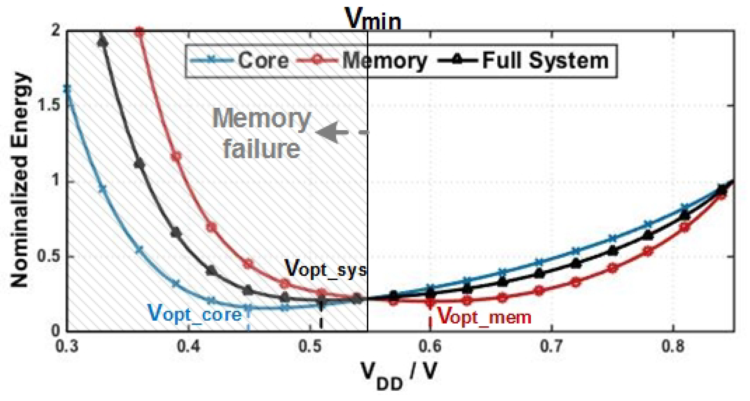
Besides, since the optimal supply voltage (
) is determined by the balance between dynamic and static energy components, computational units with different dynamic/static breakdown could have distinctive
. Zhai et al. [
10] showed that SRAMs, commonly used for caches, have a higher
than processors, by approximately 100 mV. It is caused by the relatively high leakage component of cache energy, a trade-off associated with their large size and high density. Our normalized energy simulation in
Figure 1 illustrates this effect using device parameters from 16 nm FinFET technology process [
11] and activity parameters from Gem5/McPAT simulator [
12,
13]. If we normalize the energy consumption of the logic core and the on-chip memory blocks at nominal supply voltage (850 mV in the 16 nm FinFET process), we can obtain the energy scaling trend as a function of the supply voltage [
14]. Apparently, the core energy minimizes at
around 450 mV, whereas memory energy minimizes at
around 600 mV. This result also indicates that in a NTC system where only a single supply voltage is available, both the core and the memory have to compromise to yield a unique optimal voltage (
) for the full system as indicated in
Figure 1.
As leakage increases with respect to switching energy, it becomes more efficient to run faster, hence
is shifted higher. Usually, SRAM cache can run with optimal energy efficiency at a higher speed than its surrounding logic [
1]. The minimum operating energy is achieved at the point where the switching and leakage components are balanced. At voltages higher than the NTC operating point, switching energy dominates. Below that, leakage energy dominates. Thus, the optimum operating point is usually slightly above the threshold voltage [
15].
2.2. Memory Reliability in NTC
Another critical issue that limits NTC from achieving the optimal energy efficiency is its degraded reliability. Compared to the super-threshold operation at the nominal supply voltage, near-threshold operation is more susceptible to process variation [
16,
17], supply noise [
14], and temperature fluctuations [
18] (PVT), especially for the memory blocks in NTC, due to their minimum-sized devices and large array numbers. As indicated in
Figure 1, the minimum voltage that allows reliable memory operation (
) could exceed
and often dictates the actual supply voltage [
16,
19], pushing the NTC system further away from its optimal efficiency point.
For NTC operation, 8T SRAM has been proposed as an alternative more reliable memory cell structure than 6T SRAM, but it involves trade-offs between power, area and performance. Although 6T SRAM cell is indeed more vulnerable due to mismatches between the transistors in the cross-coupled inverters [
20], it can be designed to overcome its vulnerability and work reliably in NTC with voltage boosting topology. 6T SRAM cell also leaks at least 4.5% less, and a single cell is over 30% smaller in area than 8T SRAM cell, which indicates that 6T SRAM cell remains an appealing choice for a NTC with voltage boosting SoC [
21].
2.3. Dual-Supply Architecture for Voltage Boosting
The underlying premise of NTC is that workloads can be effectively parallelized so that operating large number of energy-efficient NTC cores can deliver higher throughput at the same power budget, thus overcoming the curse of “Dark Silicon” [
22]. However, single thread performance is needed in some cases to overcome “Amdahl bottlenecks”, such as inherently serial code regions, lock contention, communication overheads, and long-tail latency distribution in servers. To mitigate the severe negative impact of single-thread performance in NTC, the implementation of dual supply rails have been proposed to temporarily boost the supply and the operating frequency of NTC processors in 10s of clock cycles [
17].
Several key facts have emerged from earlier development of NTC techniques so far: (1) energy efficiency compromise exists in single-supply NTC systems due to different for core and memory; (2) memory reliability limits further lowering of the supply voltage to achieve energy optimality; and (3) dual-supply architecture addresses a fundamental shortcoming of NTC’s single-thread performance through voltage boosting.
In our paper, we aim to achieve better energy efficiency in NTC processors by opportunistically tapping the wasted energy due to the single-supply and memory constraints. Our topology takes advantage of the dual-supply architecture originally proposed for voltage boosting and extends it to gain additional energy savings.
3. Asymmetric Memory Reliability
The critical role that memory reliability plays in NTC systems demands an in-depth examination of the underlying mechanisms contributing to memory failures at near-threshold voltages.
The most common memory structure used in on-chip caches is a 6T SRAM cell, which is presented in
Figure 2a. It consists of a cross-coupled inverter pair and two access transistors. The inverter pair that contains pull-down (PD) and pull-up (PU) transistor is used to store bit 0 or 1 through positive feedback, and the access transistor are controlled by the wordline (WL) to connect the internally-store bit value to the bitline (BL). Typical read and write operations of the SRAM array follow different well-defined control signal sequences [
23]. During a read access, BL and
are first pre-charged to
. Then, WL goes high, so that Q and
drive data through the access transistors (PG) M5 and M6 to split up the BL and
, and the voltage difference between BL and
is sensed by a sense amplifier (SA) to resolve the read data. During a write access, BL and
are driven to the complementary input data by a write driver, and WL turns on PG to drive the data into the internal storage nodes. Due to the read and write coupling, the sizing of PG, PD and PU is an argument parameter for SRAM access reliability.
To evaluate the reliability property of 6T SRAM cell under low supply voltages, we first look at its static noise margin (SNM) as a function of supply. The SNM criteria are widely used to characterize the static stability of SRAM cells. The static noise margins for hold (HSNM), read (RSNM), and write (WSNM) can be obtained by overlapping the voltage transfer curves (VTC) of the cross-coupled inverters within a cell, often called the butterfly curve [
24]. The test circuits to measure these SNM metrics are shown in
Figure 2b–d, where the cross-coupled feedback loop is intentionally broken to simulate different biasing conditions during hold, read, and write operations. The resulting butterfly curves are conceptually illustrated in
Figure 2e–g. The noise margins are extracted from the butterfly curve as the diagonal distance of the biggest square that can fit inside the butterfly curve. We can analyze the shapes of the butterfly curves. For example, during the read operation,
and
are pre-charged to
, which pull the VTC higher and cause it to move slowly to the bit-0 low voltage level as in
Figure 2f for read, compared to the curves in
Figure 2e for hold. Similarly, during write, one side of the bitlines is driven to ground, the other to
. As a result, one of the VTCs corresponding to the ground side switches to low voltage level sharply, as shown in
Figure 2g.
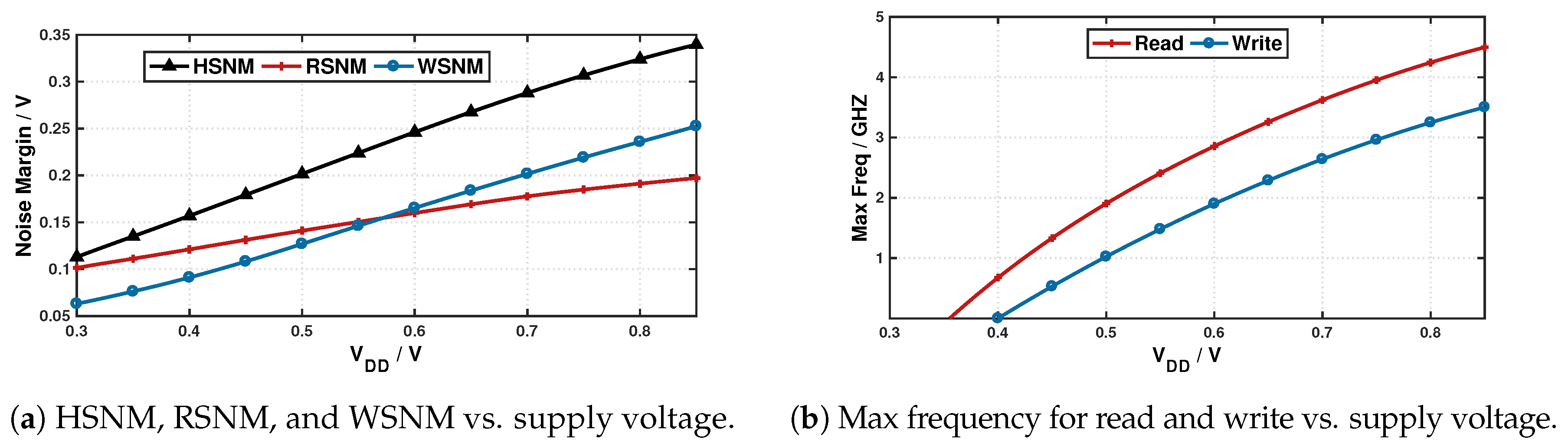
To obtain a quantitative measurement of the SNMs across a wide supply range, we sweep the supply voltage from 0.3 V to 0.85 V, the nominal supply voltage of the 16 nm predictive technology model (PTM) using customized sizing configuration.
Figure 3a presents the different noise margins as a function of the supply voltage. Interestingly, read stability and write stability show opposite behaviors at different end of the voltage spectrum: when the supply voltage is high, WSNM is higher than the RSNM, while, at lower supply voltage, the roles are flipped with RSNM being higher than WSNM. Our results corroborate with previous work on write margin analysis [
25], and hence we hypothesize that write operation fails earlier than read when we lower the supply voltage.
Figure 3b shows that read operation indeed outlasts write, and it is possible to reliably read from the SRAM cell at near-threshold voltages where write would have already failed. Hence, if we could switch power supply to a lower voltage for SRAM read operation, a significant power will be saved while maintaining reliable operation. Similar results for different voltages for read and write SRAM reliability have also been observed experimentally in 14 nm devices [
26], where read failure rate is reported to be lower and so is its minimum error-free voltage.
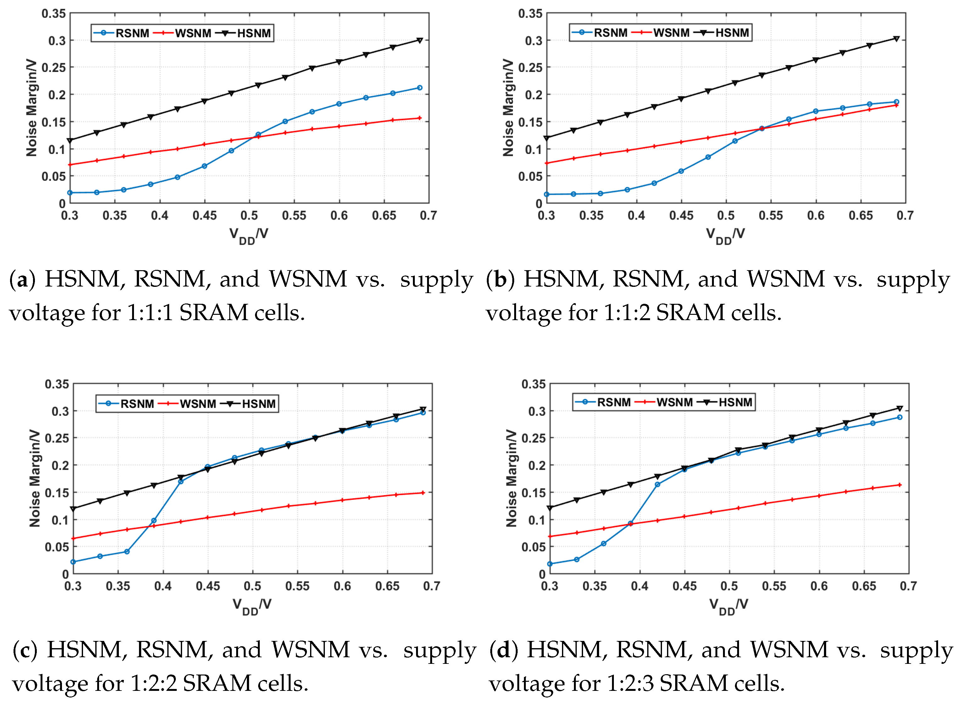
Additionally, we validate the PG, PU, PD transistor sizing impact on static reliability characteristic for SRAM cells in deeply scaled technology, 7 nm ASAP PDK [
27]. We sweep the supply voltage from 0.3 V to 0.7 V with several popular standardized SRAM cell ratios. The SRAMs implemented in our test have the fin-ratios (PU:PG:PD) of 1:1:1, 1:1:2, 1:2:2 and 1:2:3. With the variance of fin-ratios, the static noise margins change as shown in
Figure 4a–d. The RSNM and WSNM will always flip while in the different voltage domain. Interestingly, as the PG ratio increasing, the intersection between RSNM and WSNM moves to sub-threshold voltage domain and the upper side of it approaches to RSNM. Associated with above discussion, the 1:1:1 and 1:1:2 SRAM cells in 7 nm process may retain the similar static reliability property and supply voltage demands for read and write separately. In conclusion, we believe this asymmetric reliability property could open new opportunities to improve energy efficiency of NTC processors even in high-end deeply scaled technology process.
4. Opportunistic Dual-Supply Switching
Our circuit-level analysis of the SRAM reliability in
Section 3 reveals new energy saving opportunity by leveraging the asymmetric read/write behaviors: if we can separate the read operations from the write operations and set the memory block to lower supply voltages during read-only transactions, the processor could potentially more closely approach its optimal supply voltage that minimizes full-system energy efficiency, especially in a NTC processor as illustrated in
Figure 1. Moreover, it may be possible to take advantage of the dual-supply architecture that has already been proposed for boosting NTC’s degraded single-thread performance [
17] by connecting the memory blocks to dual supply rails and alternating their supply voltages based on transitions between read and write instruction sequences. This forms the basic idea behind our proposed opportunistic dual-supply switching scheme for the memory systems in NTC processors. In this section, we analyzed cache behavior characterization of a usual general purpose computational-intensive workload SPEC2006 and data-intensive workload PARSEC to leverage the opportunistic improvement potential upon the read/write intensity in full system simulation. We then discuss the design considerations and the implementation details of our method.
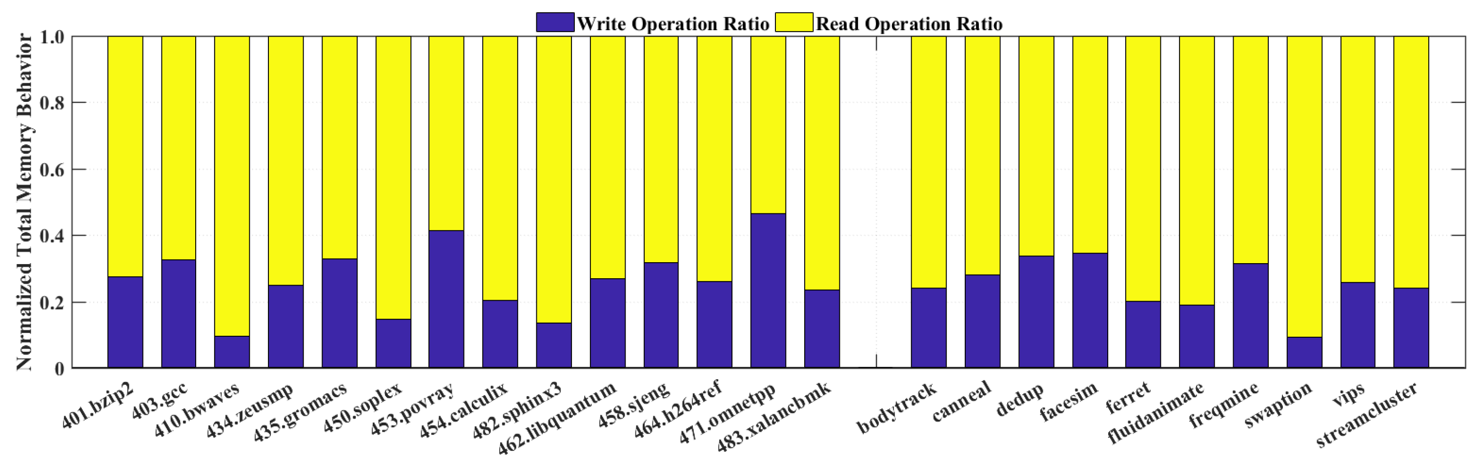
4.1. Memory Behavior Characterization of Workload SPEC2006
According to the dual-supply switching scheme discussed above, the read and write instruction sequences are crucial, because the ratio of read operations and write operations and their orders would influence the switching behavior and energy reduction opportunity. The larger percentage of read operations over total memory behaviors means that there will be more chances to lower the voltage supply to
to decrease the energy consumption. To investigate such memory behavior characteristics, we selected diverse general-purpose benchmark SPEC2006 and PARSEC, which are computation-intensive and data-intensive respectively. In our study, we used Gem5 cache trace probe to analyze the data request between processor and cache to get the approximate portion of read and write operations within diverse benchmarks. Several selected representative workloads from the SPEC2006 suites are evaluated on X86 system which is configured as in
Table 1, with a three-level cache hierarchy: 64kB L1-cache (32 kB I-cache and 32 kB D-cache), 256 kB L2cache and 2 MB Last Level Cache (LLC).
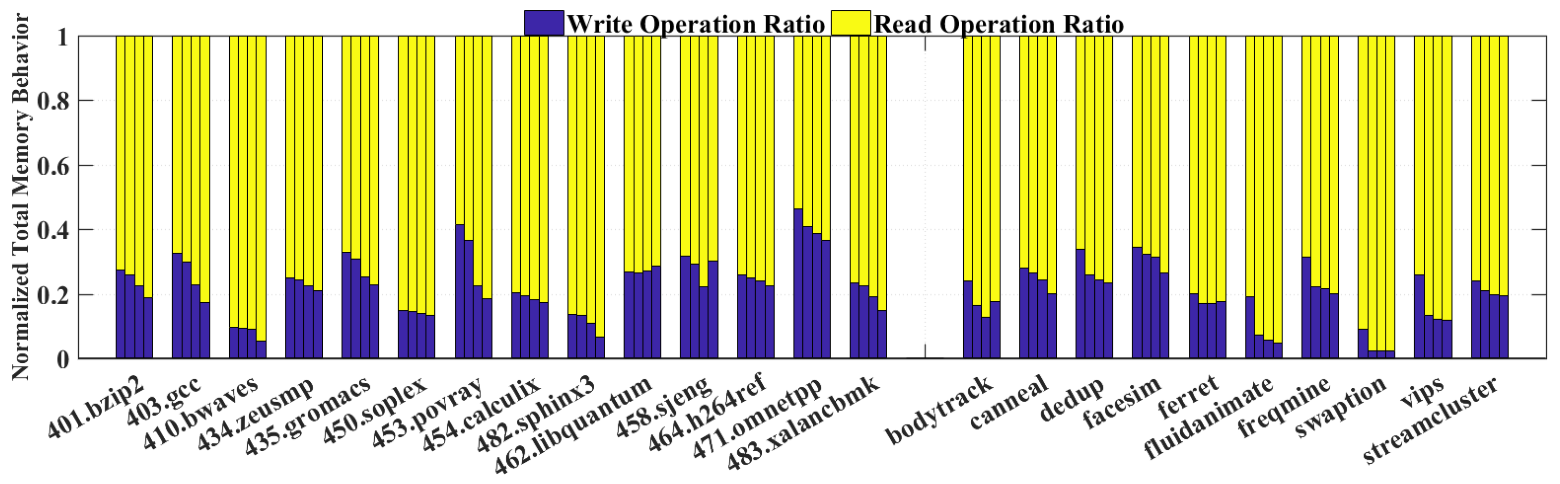
Figure 5 shows the ratio distribution between total read and write operations. Interestingly, the read operations of most workloads among both SPEC2006 and PARSEC take more than 70% of all memory operations, which illustrates that it has a promising potential to let our switching architecture dominates the voltage supply with
instead of
.
4.2. Naive Greedy Switching
In a system with dual supply rails, each component can be connected to either rail via power switches that are controlled by enabling/disabling signals. However, switching between these supply rails incurs non-negligible latency and energy costs. For example, according to one such dual-rail application switching between 400 mV and 600 mV in 32 nm process [
17], the rise time is approximately 9 ns and the fall time 7 ns. Therefore, overheads have to be accounted for when evaluating the potential benefits of dual-supply switching for the memory blocks in NTC.
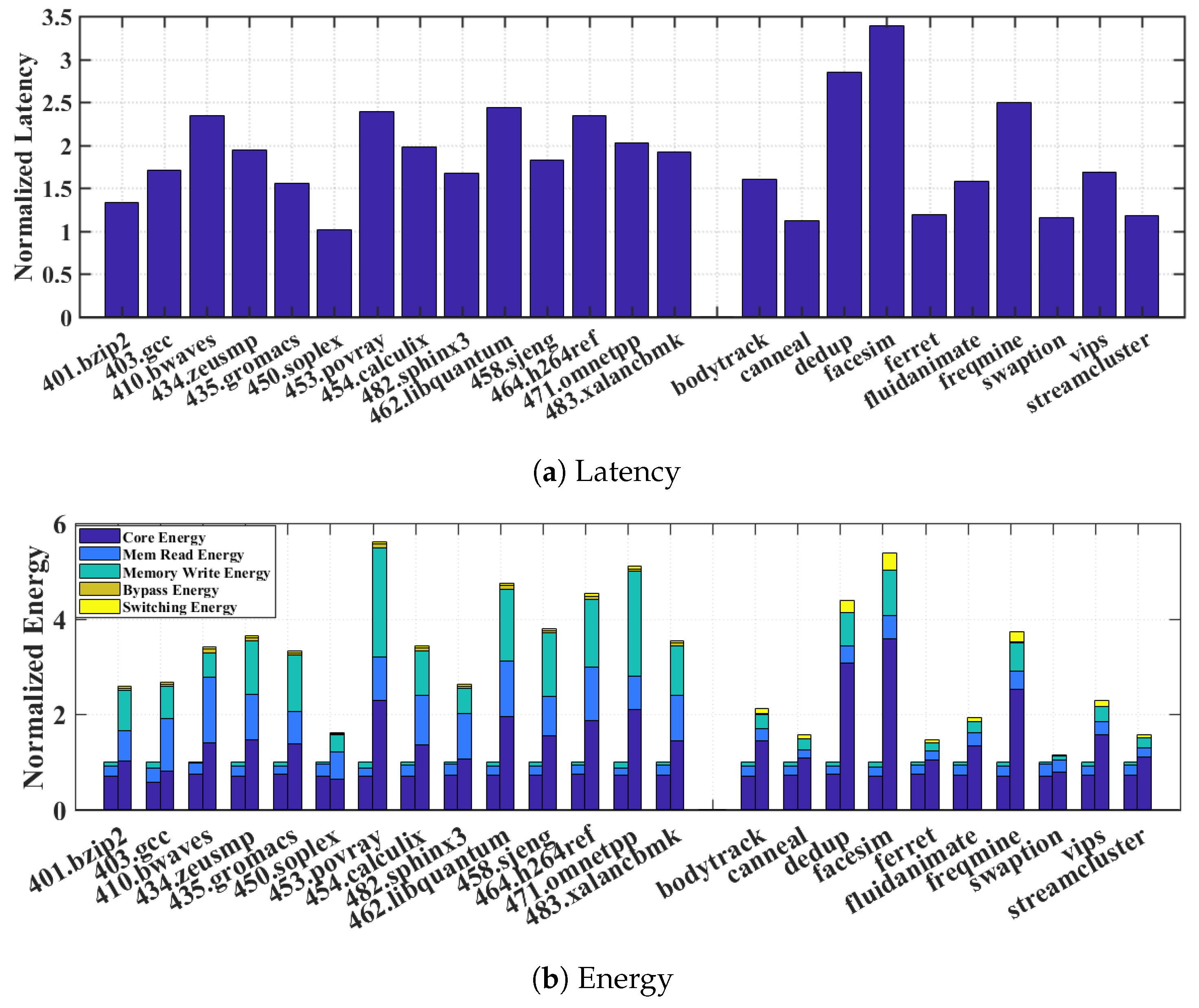
Let us first evaluate a naive approach of greedy switching—the memory supply is set to
mV whenever there is a read transaction and to
mV whenever there is a write transaction. We pick these voltage levels because
is close to
in this technology process, and
is the nominal supply voltage. We use the NTC configuration with a single supply voltage at
mV as the baseline case for comparison. We use the transition delay numbers from previously published dual-supply architecture for our estimation [
17].
Figure 6a reveals that execution latency can rise significantly due to the additional transition time of the supply switching. The latency increase can be as much as 60–70% for most SPEC2006 and PARSEC benchmarks. In addition to the latency penalty,
Figure 6b indicates that naive greedy switching results in significant energy overheads on top of the normal energy consumption broken down for core, memory read, and memory write.
Several sources contribute to these overheads: the core and memory energy overheads are due to increased leakage while the memory waits the rise time from to ; and the power switch overhead refers to the additional energy lost due to the heat dissipation on the parasitic resistance of the power switch. It is worth pointing out that, in the naive greedy switching scheme, the reason that memory read and write energies increase compared to the baseline is because we account for the fact that memory read now happens at and write at , compared to the NTC baseline where both operate at . This also explains why the core energy decreases since in the naive greedy switching, it operates at .
The overwhelming latency and energy penalty suggest that the naive greedy approach of opportunistically switching the memory supply to during read transactions and to during write transactions is prohibitively costly, thus defeating the original purpose of improving system energy efficiency. To find a more practical approach, we analyze the detailed penalty distribution by comparing different benchmarks. We observe that in benchmarks that exhibit smaller latency and energy penalty, such as 401.bzip, 450.soplex, and 482.sphinx3, there are much fewer supply switching activities. Since every switching incurs a fixed one-time latency and energy cost due to transition delay, ideally a long consecutive read sequence is preferred to amortize the cost and reap more energy benefits from staying in that minimizes core energy per operation.
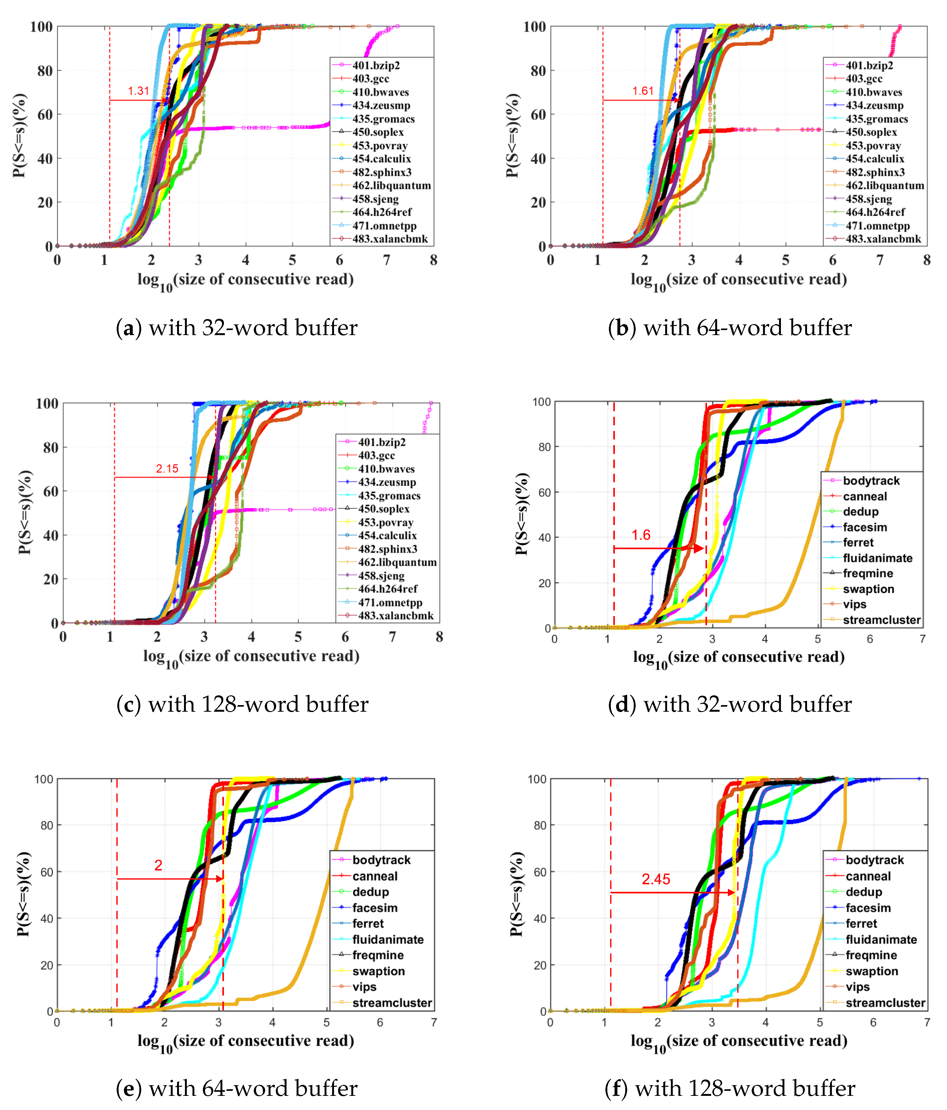
4.3. Long Consecutive Read Opportunity
Based on our study of the naive greedy switching overhead, it is clear that to maximize energy saving opportunity using dual-supply switching, we need long consecutive read sequences which are not interrupted by write operation in the memory transaction trace. To visualize and identify such opportunity from the memory transaction traces, we propose a quantitative measure using the cumulative distribution function (CDF) of consecutive read sequences to represent the long consecutive read sequence potential (LCRSP) in different benchmarks, as defined by Equation (
1).
where
is the cumulative probability function of consecutive read sequence the represents the entire read operations released from CPU or higher level cache when the benchmark is executed; n represents the set number of read sequence groups with unique consecutive read sizes;
s equals to
;
t is the number of occurrence of sequences with each unique consecutive read size; and
r is the total number of read operations.
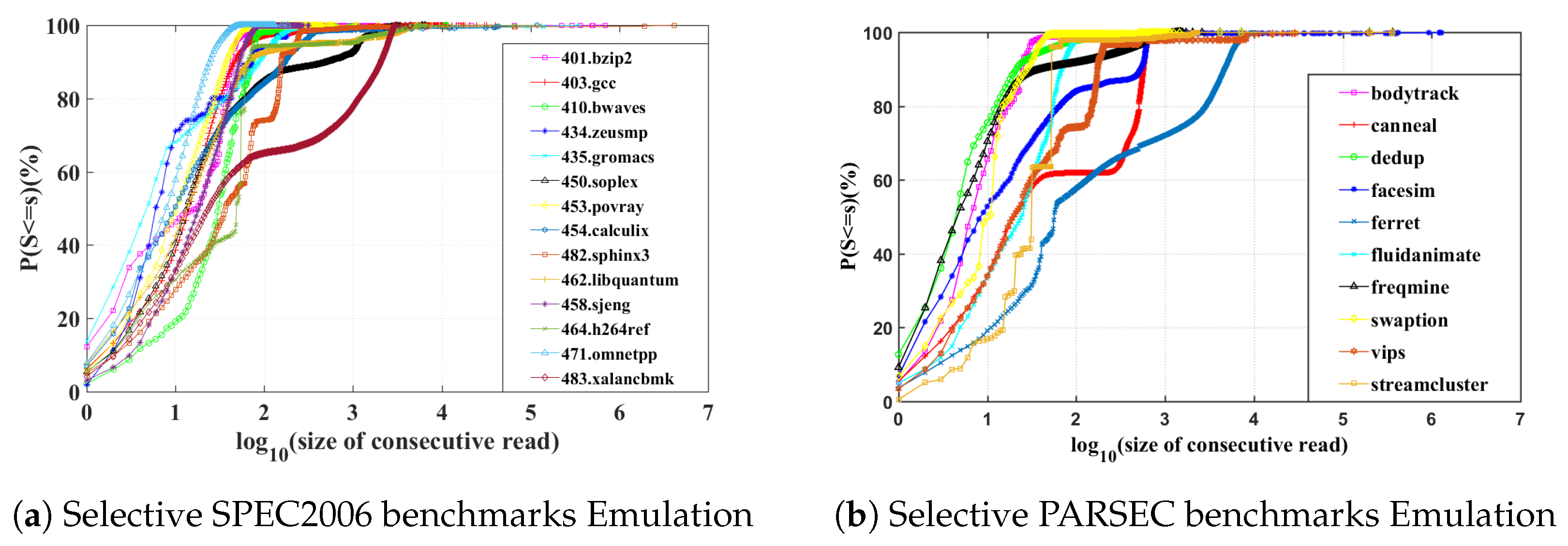
Using the definition in Equation (1), we can plot the CDFs of consecutive read sequences generated by executing different SPEC2006 and PARSEC benchmarks, as shown in
Figure 7a,b. If we look at three characteristic points where the CDF crosses 20%, 50%, and 80% probability, we find that the greater the value of the horizontal axis corresponding to these percentages, the higher LCRSP the benchmark has according to its cache trace. For example, in 483.xalancbmk, these three CDF characteristic points are approximately
= 18.718%,
= 50.353% and
= 79.99%, which means 79.99% of the trace has a consecutive read size of
or smaller. It suggests that 483.xalancbmk has many long consecutive read sequences, therefore is a good candidate for dual-supply switching. Conversely, similar measure would suggest that the cache trace of 435.gromacs’s has a poor portion of long reads, aggressively switch the dual-supply power will bring unexpected cost.
Figure 7a,b indicates SPEC2006 and PARSEC benchmarks are diverse and the opportunity to save energy is unevenly distributed. Interestingly, we note that PARSEC benchmarks generally show higher potential thanks to the longer consecutive read sequences in PARSEC’s data-intensive workloads.
4.4. Write Aggregation Buffer (WAB)
Since the read-to-write transition delay is the culprit that dominantly contributes to the latency and energy overheads shown in
Figure 7a,b, we need to improve the LCRSP of different benchmarks by reducing the number of read-to-write transitions. This is equivalent to reducing the number of write operations interrupting the long consecutive read sequence. Therefore, we propose a micro-architecture unit called write aggregation buffer (WAB) and Write back aggregation buffer (WBAB) to accumulate write operations and stop releasing them frequently from disturbing consecutive reads.
The micro-architecture structure of our proposed WAB and WBAB is based on write buffer [
28] design used in cache architecture of conventional CPU systems such as Intel Xeon and AMD64. In conventional processor, a write buffer can hold the data temporarily and stop it being written from the higher-level cache (for write backward) or to the next-level cache or the main memory (for write forward). It allows the lower-level cache to service the subsequent read requests without waiting for long write transactions to complete at slow main memory. We enhance the conventional write buffer design with aggregation functionality to accumulate write transactions together to a specific length and release multiple write requests to the global cache access sequence all at once. During the WAB releasing period, read transactions still have higher priority. When a read request is issued to the global access sequence, the write release operation at the WAB would halt and wait for reads to be completed. Actually, this policy increases the duration of write-level power switch-on, but reduces the supply switching activities in disguise. Additionally, to guarantee the reliability of WAB/WBAB access, the supply voltage of WAB/WBAB is connected to
.
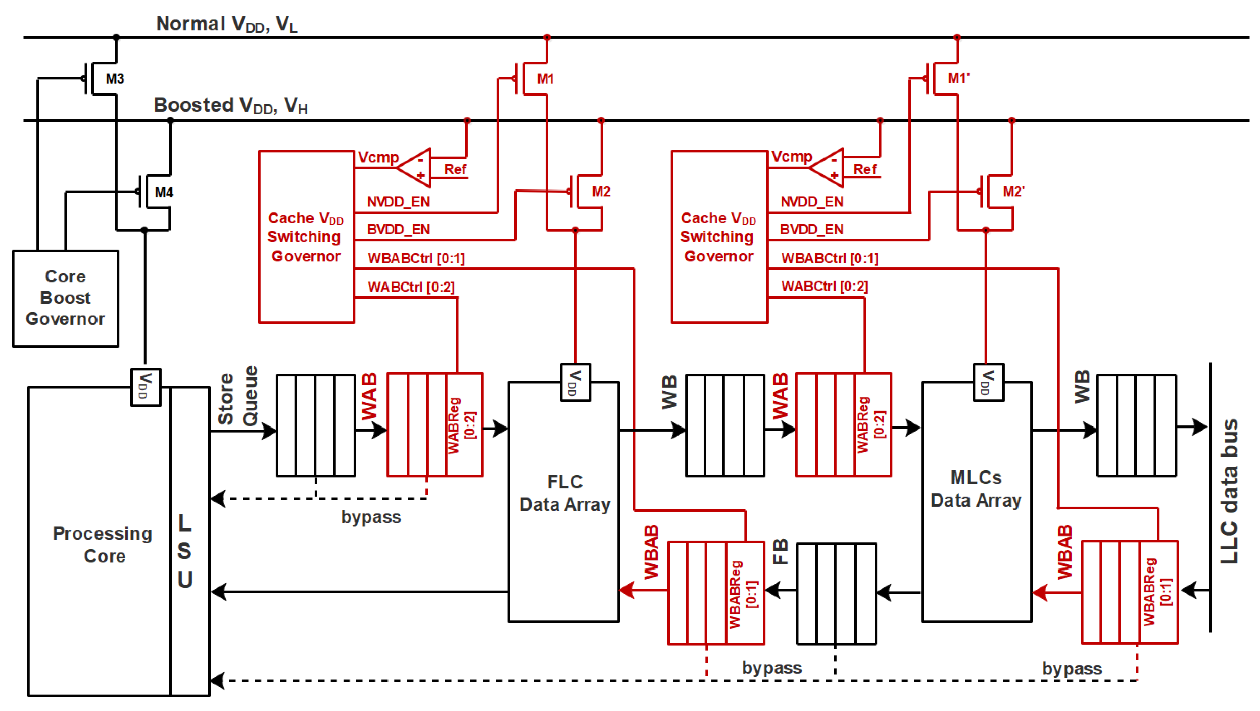
The system diagram in
Figure 8 illustrates how our proposed WAB structures are inserted at the L1 and L2 cache hierarchy in a NTC processor with dual supply rails. The components highlighted in red are the WABs and their associated auxiliary circuits to enable the opportunistic dual-supply switching. Inserted between Write Buffer (WB) and L1 D-cache is one WAB that aggregates the write request from the processor core side. Another WAB, labeled as Write Back Aggregation Buffer (WBAB), is inserted between Write Back Buffer and Fill Buffer (FB), and it accumulates the write back requests from lower level cache side. However, WBAB does not have to yield to read transactions because of the CPU scheduling priority. Accompanying these buffers are auxiliary circuitry including power switches, voltage comparators, and dual-supply switching controllers. The cache voltage supply switching control signal ports contains voltage comparison signal,
; Normal Voltage (
) enable signal,
NVDD_
EN; Boost Voltage (
) enable signal,
BVDD_
EN; Write aggregation buffer control register,
WABCtrl; Write back aggregation buffer control register,
WBABCtrl. These two control register ports of
switching controller connect with WAB and WBAB control register ports,
WABReg and
WBABReg, respectively. The connectivity between these ports consist of
WABRb to
WAB_
Rel_
bit,
WABFb to
WAB_
Full_
bit,
Read_
Rq to
W_
Y_
bit,
WBABRb to
WBAB_
Rel_
bit and
WBABFb to
WBAB_
Full_
bit.
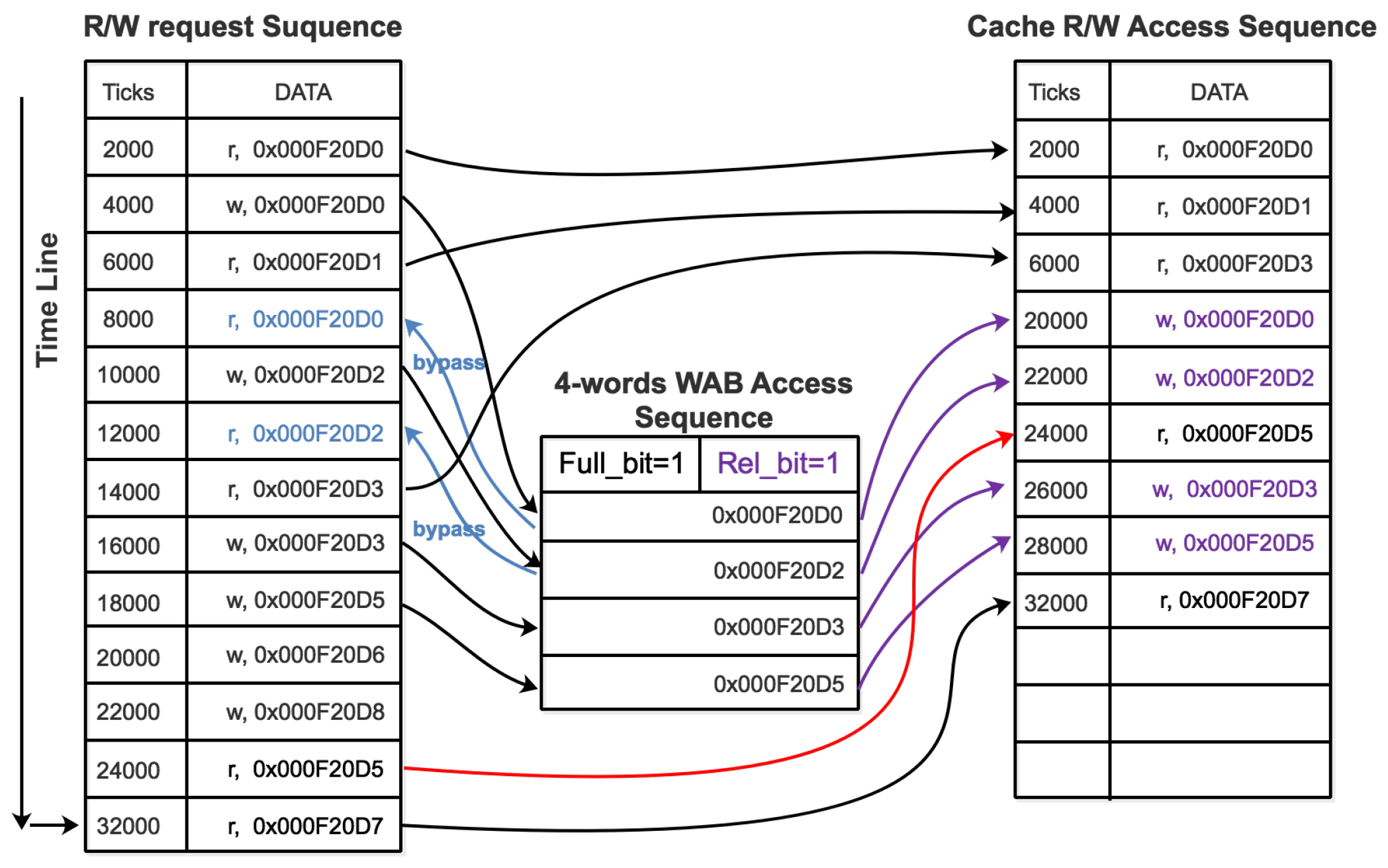
The above pseudo code in Algorithm 1 and the illustration of an example R/W access sequence execution re-ordered by WAB in
Figure 9 explain how the dual-supply switching controller works with the WAB and WBAB. When WAB/WBAB is not filled, the read requests are released to the cache R/W access sequence directly and the write requests are forwarded to WAB/WBAB. Meanwhile, the bypass structure responses directly to the read request, so direct access to the cache is not needed for a read after write (RAW) data access. Once WAB/WBAB reaches a fixed buffer length of aggregated write operations, the
WAB_
Full_
bit or
WBAB_
Full_
bit will be set up to 1, indicating WAB/WBAB are filled. Followed by this, the dual-supply power switches are activated. The transistor M1 will be turned off and M2 turned on. During
to
transition (from 450 mV to 850 mV in our example), WAB/WBAB cannot release aggregated write operations to the global cache access sequence, since reliable write is not guaranteed in that voltage transition interval and corresponding latency may incur. We place a voltage comparator to determine whether
reaches a safe level for write. When that condition is met,
will turn to 1 and set the
WAB_
Rel_
bit or
WBAB_
Rel_
bit, which in turn activates the write release operation at WAB and WBAB. If WAB and WBAB release their aggregated write operations simultaneously, they should follow the CPU tick schedule to manage the order of each single write operation in the aggregated write sequence. Please note that by setting
at a high voltage level of 850 mV, our proposed system architecture is fully compatible with voltage boosting for NTC processors, and allows our switching scheme to run concurrently with voltage boosting if needed.
| Algorithm 1 switching governor algorithm. |
| Input: WABFb, WBABFb and |
| Ouput: NVDD_EN, NVDD_EN, WBABRb, Read_Rq and WABRb |
| 1: |
| 2: |
| 3: |
| 4: |
| 5: // Read request bit |
| 6: if Request read then |
| 7: // set W_Y_bit to 1 |
| 8: WAB Write halt and wait for reads |
| 9: else |
| 10: // set W_Y_bit to 0 |
| 11: if WAB_Full_bit == 1 | WBAB_Full_bit == 1 then |
| 12: // set NVDD_EN to 1 |
| 13: // reset BVDD_EN to 0 |
| 14: else |
| 15: // set NVDD_EN to 0 |
| 16: // reset BVDD_EN to 1 |
| 17: end if |
| 18: if == 1 then |
| 19: if WAB_Full_bit == 1 then |
| 20: // WAB release aggregated write data chuck by once |
| 21: end if |
| 22: if WBAB_Full_bit == 1 then |
| 23: // WBAB release aggregated write data chuck by once |
| 24: end if |
| 25: else |
| 26: |
| 27: |
| 28: // Hold aggregated write data chuck in WAB or WBAB |
| 29: end if |
| 30: end if |
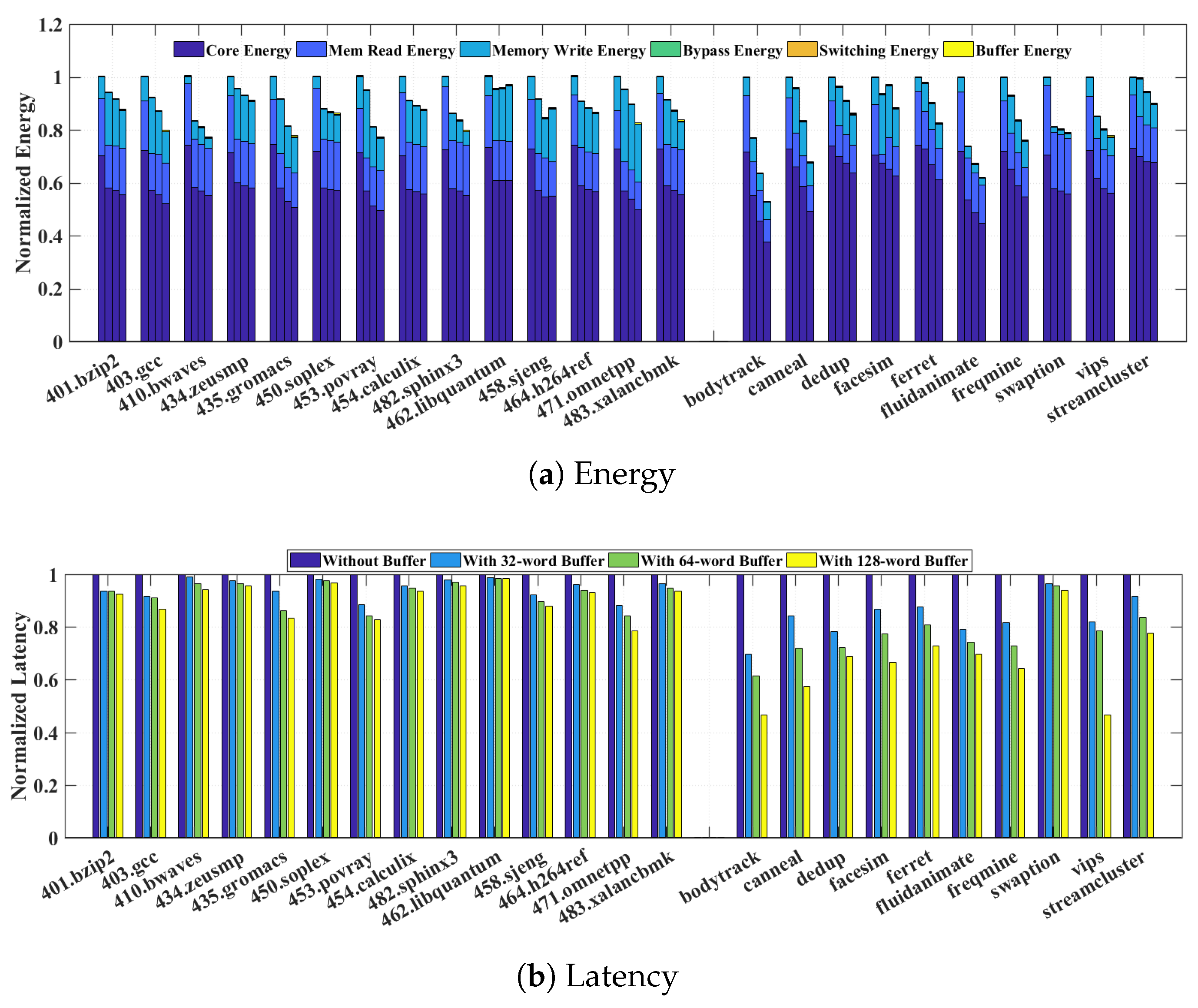
4.5. WAB and WBAB Enabled Switching
To examine the effect of WAB and WBAB to the distribution of read sequences, we compare the CDF curves of different benchmark cache traces with and without WAB and WBAB, as well as with varying WAB and WBAB sizes.
Figure 10 presents the LCRSP improvement by implementing various size WAB and WBAB among the cache traces of diverse SPEC2006 and PARSEC benchmarks.
According to the approximate mean value of X axis which means , corresponding to characteristics points 50%, we can see that after implementing WAB and WBAB, all of their CDFs experience a right shift. The abscissa of the averaged characteristic points are increased by one to two roughly. These results suggest that our proposed WAB and WBAB structure is able to universally improve the characteristics of LCRSP across diverse benchmarks that could result in to roughly longer read sequence for our opportunistic dual-supply switching scheme to exploit further energy savings. when we observe the LCRSP promotions of SPEC2006.401.bzip2, PARSEC.fluidanimate and PARSEC.streamcluster workload by increasing the WAB size, we discover that there should be a saturation border for each workload’s LCRSP improvement. The LCRSP curves of these three workloads mentioned above almost remain unchanged by implementing variant size WAB.
Meanwhile, the read and write operations that are executed by cache will also be decreased by our WAB/WBAB because of the bypass mechanism. The WAB/WBAB plays the crucial role aggregating the write operations together to the consecutive chunk as the releasing candidate and acts as the enlarged write buffer or write back buffer which are already existed in current CPU architecture as well. The immediate reuse data will not go into cache directly, but be executed in WAB/WBAB instead. Though the entire memory behavior number still stays fixed because of the constant instructions, the cache executed read and write ratio will change and provide more opportunities to switch the voltage supply to
.
Figure 11 shows the normalized read and write operations ratio variance by implementing 32-word, 64-word and 128-word WAB and WBAB from left to right, compared with original system without WAB and WBAB.


