
A Fully Integrated 2:1 Self-Oscillating Switched-Capacitor DC–DC Converter in 28 nm UTBB FD-SOI †


Abstract
:
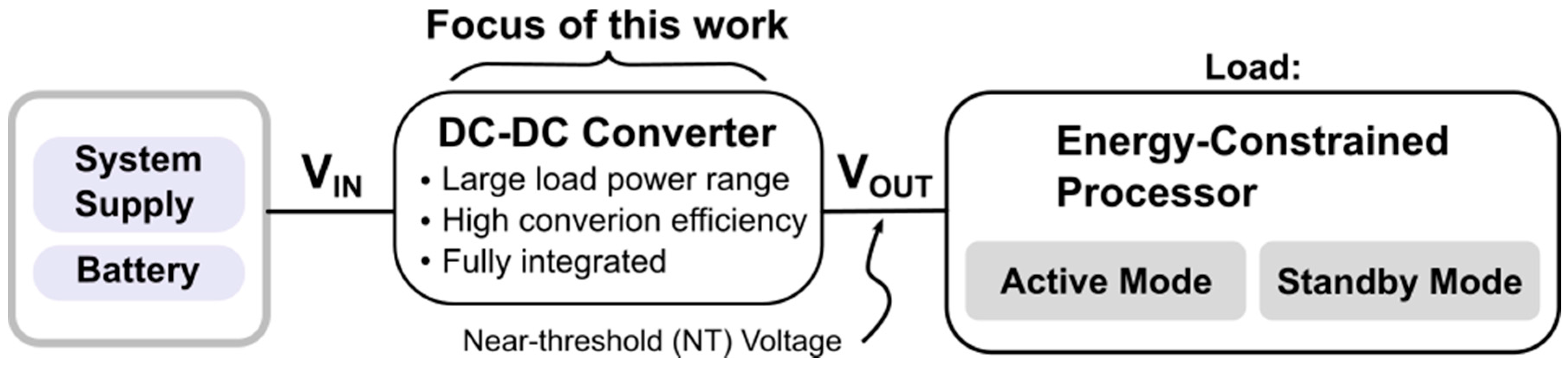
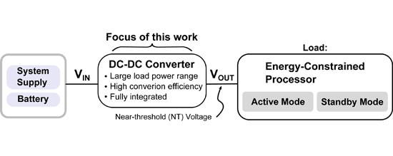
1. Introduction
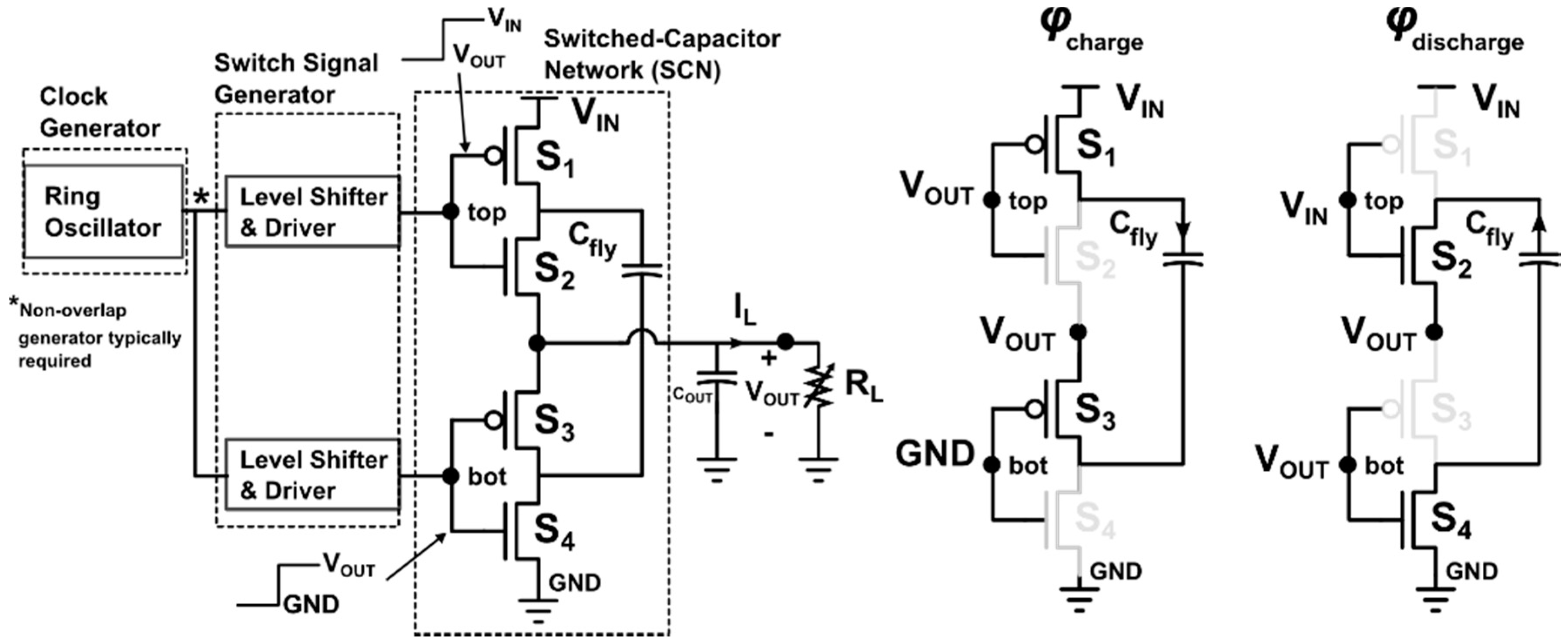
2. Self-Oscillating DC–DC Converter
2.1. Conventional Switched-Capacitor DC–DC Converter
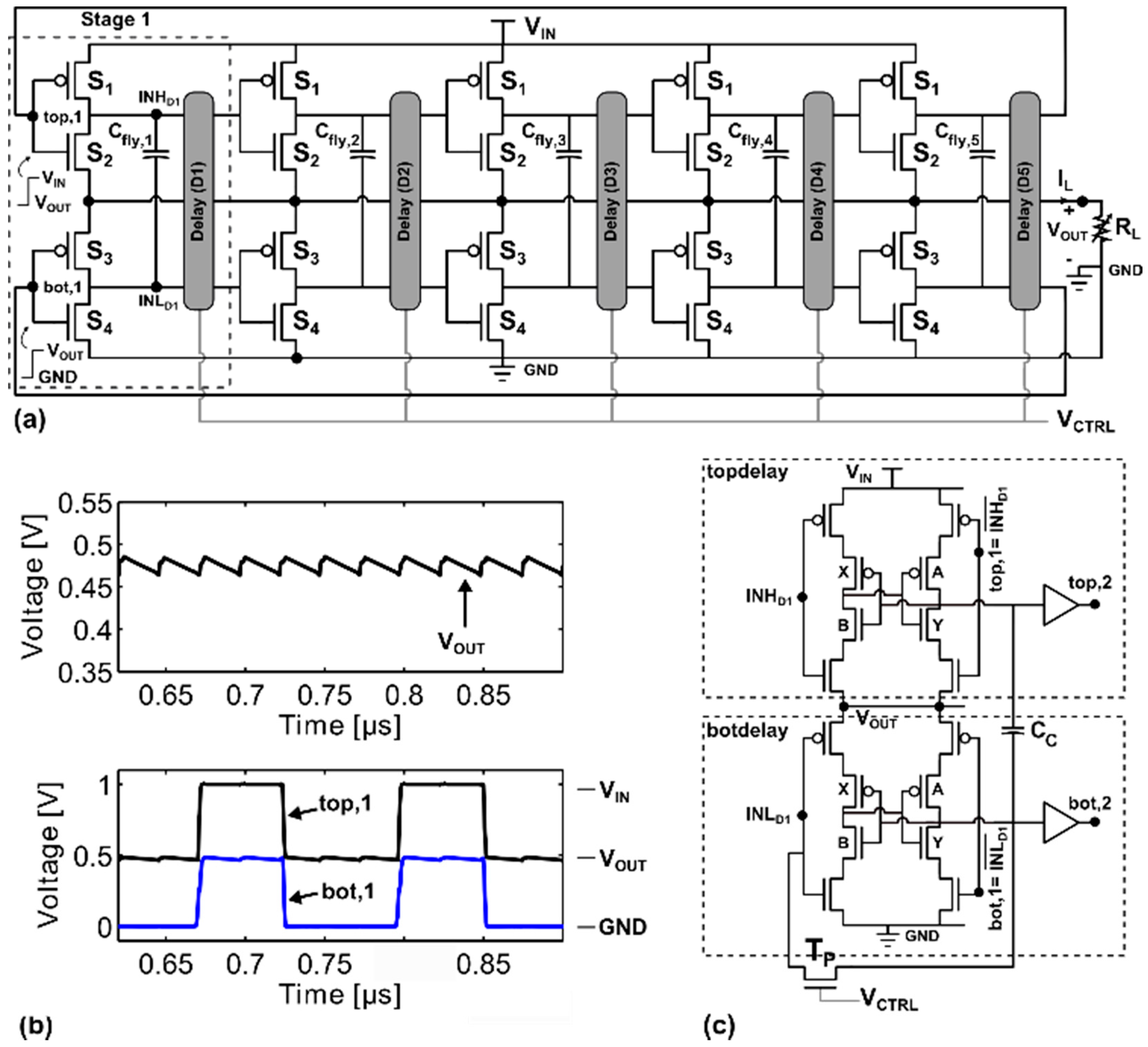
2.2. Step-Down Self-Oscillating DC–DC Converter
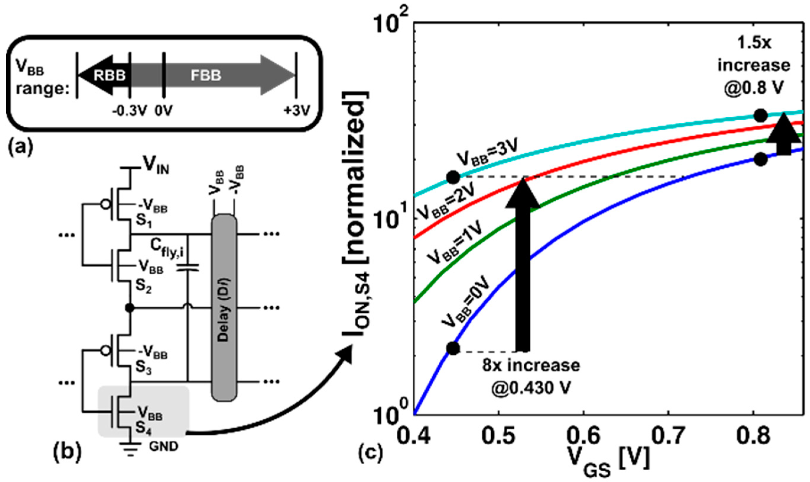
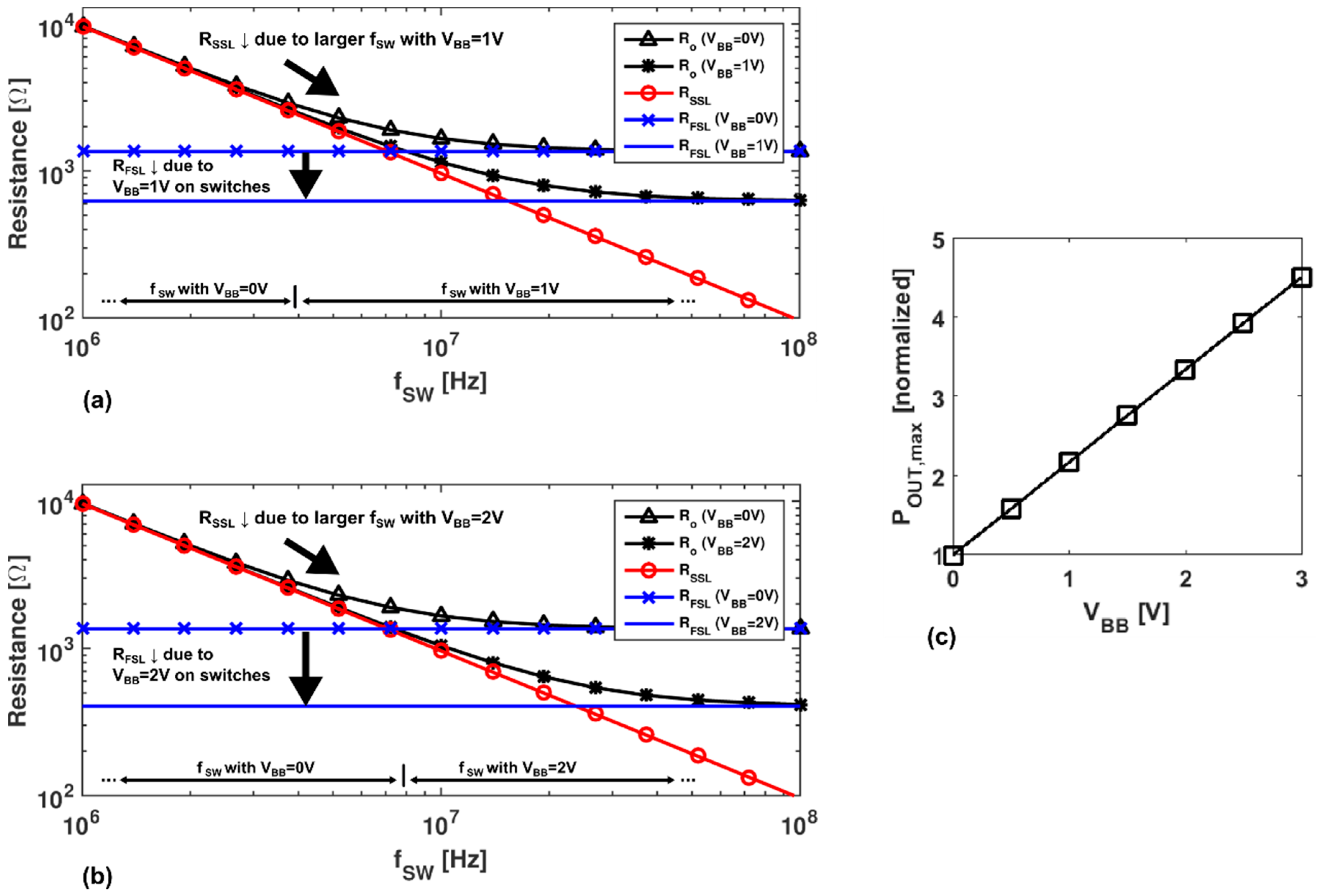
2.3. Back-Gate Biasing
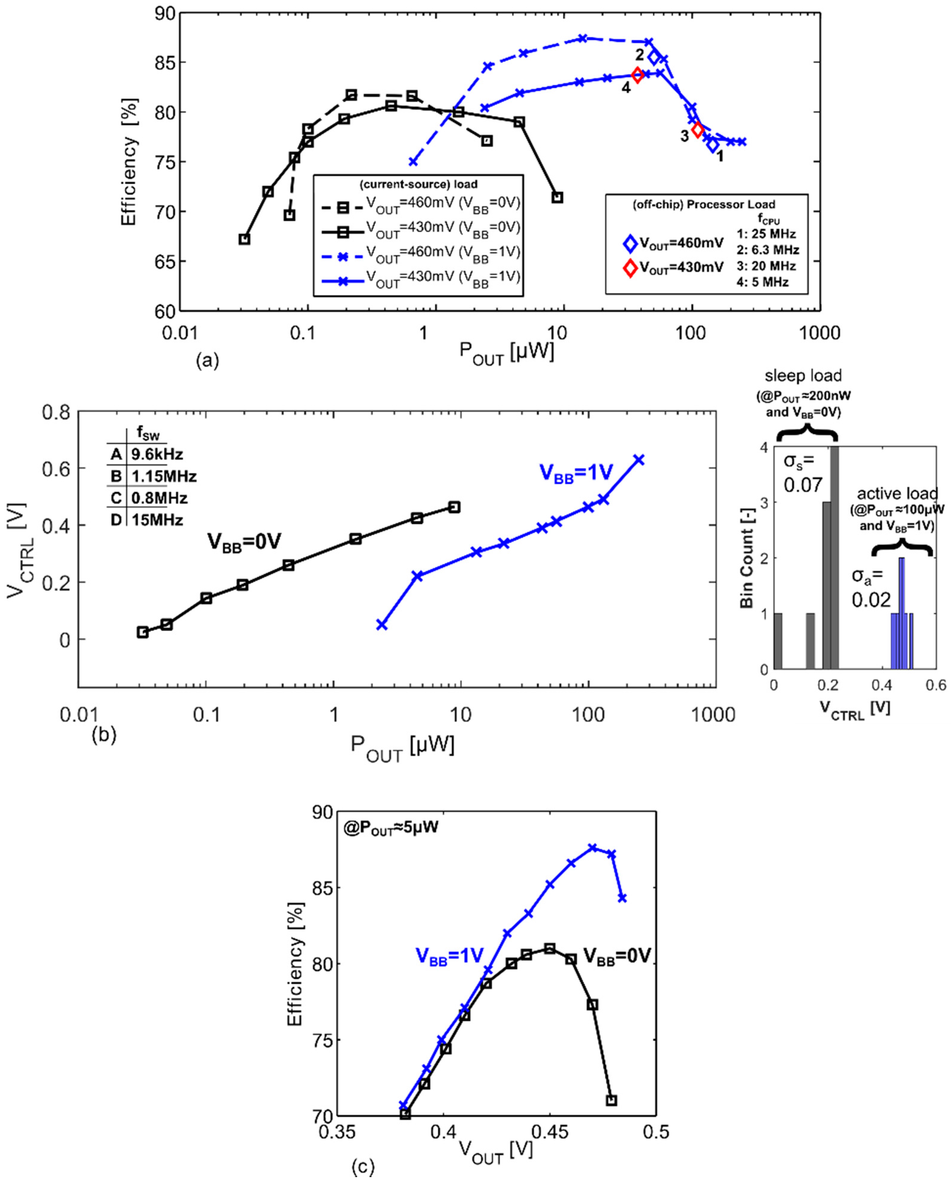
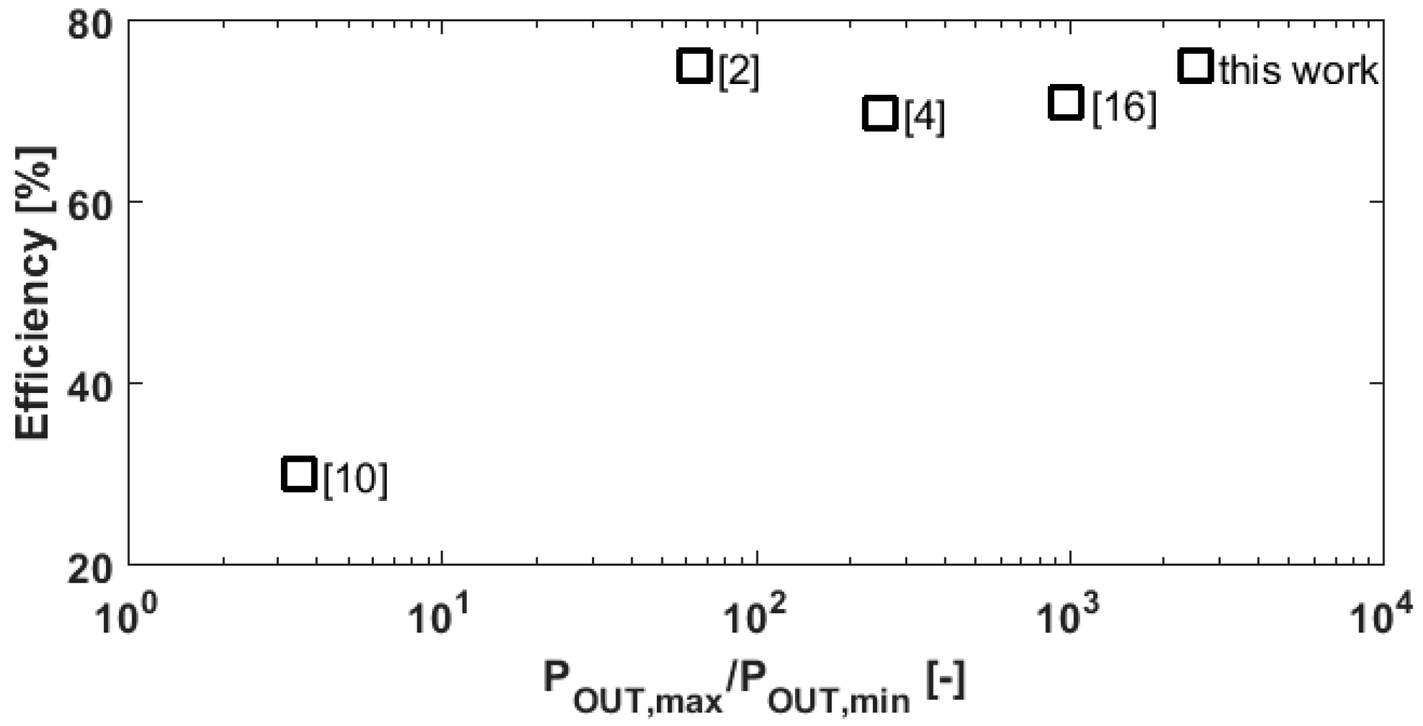
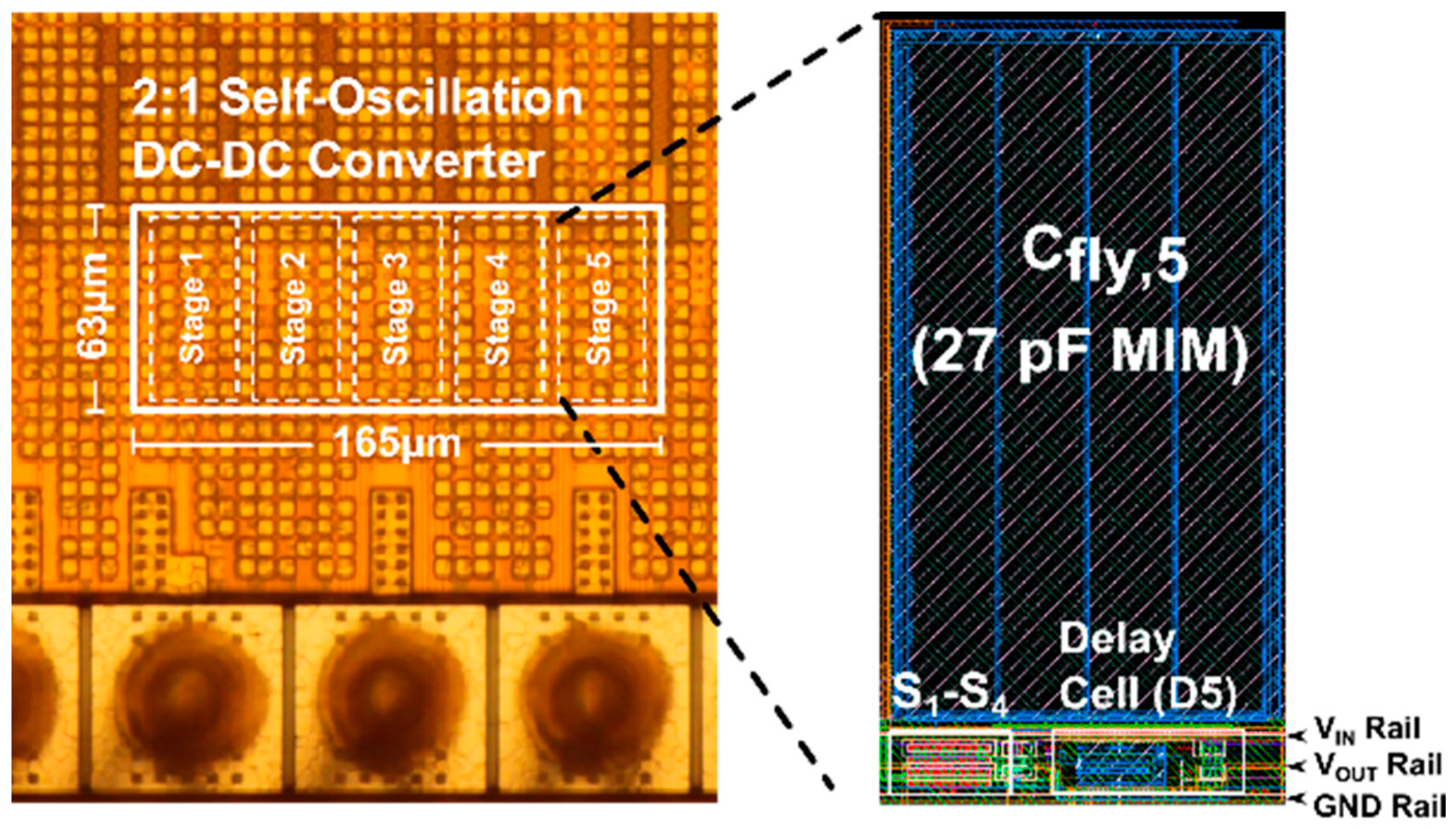
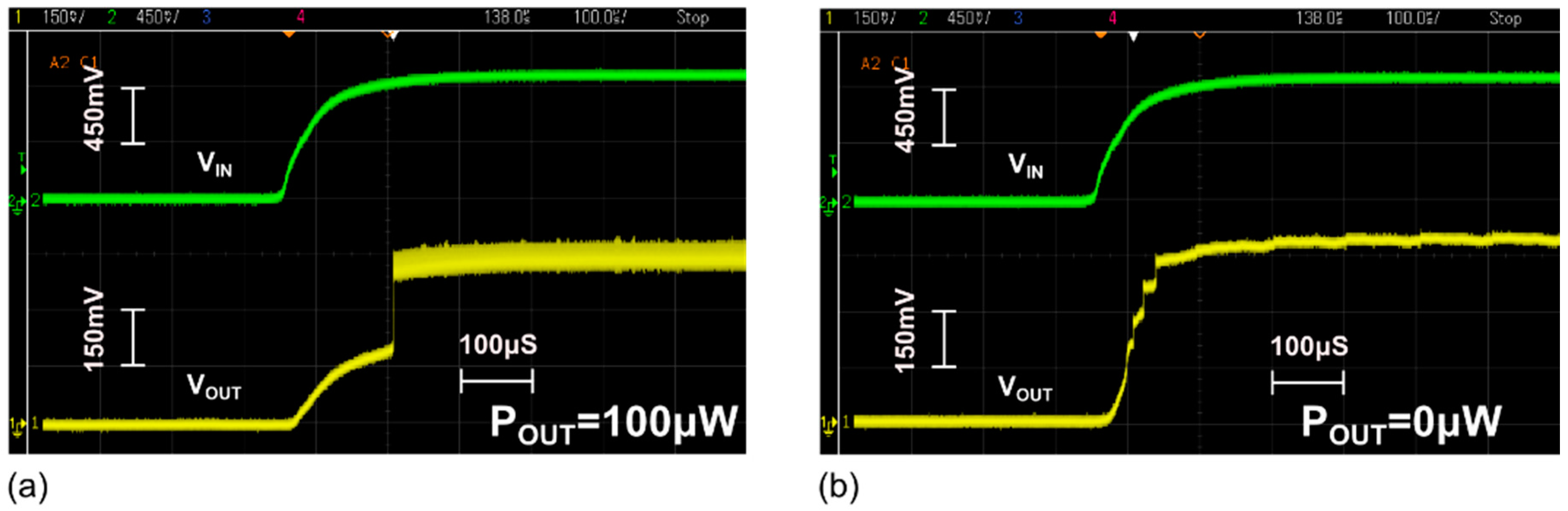
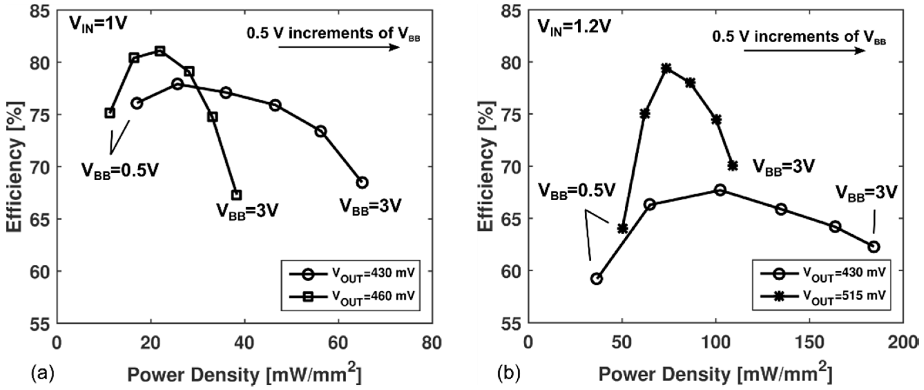
3. Measurement Results
4. Conclusions
Acknowledgments
Author Contributions
Conflicts of Interest
References
- Hiienkari, M.; Teittinen, J.; Koskinen, L.; Turnquist, M.; Kaltiokallio, M. A 3.15pj/cyc 32-bit RISC CPU with timing-error prevention and adaptive clocking in 28 nm CMOS. In Proceedings of the 2014 IEEE Custom Integrated Circuits Conference (CICC), San Jose, CA, USA, 15–17 September 2014; pp. 1–4.
- Bol, D.; Vos, J.; Hocquet, C.; Botman, F.; Durvaux, F.; Boyd, S.; Flandre, D.; Legat, J. A 25-MHz 0.4-V Sub-mm2 7-µW/MHz Microcontroller in 65-nm LP/GP CMOS for Low-Carbon Wireless Sensor Nodes. IEEE J. Solid-State Circuits 2013, 48, 20–32. [Google Scholar] [CrossRef]
- Hanson, S.; Seok, M.; Lin, Y.-S.; Foo, Z.; Kim, D.; Lee, Y.; Liu, N.; Sylvester, D.; Blaauw, D. A Low-Voltage Processor for Sensing Applications with Picowatt Standby Mode. IEEE J. Solid-State Circuits 2009, 44, 1145–1155. [Google Scholar] [CrossRef]
- Kwong, J.; Ramadass, Y.K.; Verma, N.; Chandrakasan, A.P. A 65 nm Sub-Vt Microcontroller with Integrated SRAM and Switched Capacitor DC–DC Converter. IEEE J. Solid-State Circuits 2009, 44, 115–126. [Google Scholar] [CrossRef]
- Clerc, S.; Saligane, M.; Abouzeid, F.; Cochet, M.; Daveau, J.-M.; Bottoni, C.; Bol, D.; De-Vos, J.; Zamora, D.; Coeffic, B.; et al. A 0.33 V/−40 °C process/temperature closed-loop compensation SoC embedding all-digital clock multiplier and DC–DC converter exploiting FDSOI 28nm back-gate biasing. In Proceedings of the IEEE International Solid State Circuits Conference (ISSCC), San Francisco, CA, USA, 22–26 February 2015; pp. 1–3.
- Seongjong, K.; Mingoo, S. Variation-Tolerant, Ultra-Low-Voltage Microprocessor with a Low-Overhead, Within-a-Cycle In-Situ Timing-Error Detection and Correction Technique. IEEE J. Solid-State Circuits 2015, 50, 1478–1490. [Google Scholar]
- Sarafianos, A.; Steyaert, M. Fully Integrated Wide Input Voltage Range Capacitive DC–DC Converters: The Folding Dickson Converter. IEEE J. Solid-State Circuits 2015, 50, 1560–1570. [Google Scholar] [CrossRef]
- Jung, W.; Oh, S.; Bang, S.; Lee, Y.; Sylvester, D.; Blaauw, D. A 3nW fully integrated energy harvester based on self-oscillating switched-capacitor DC–DC converter. In Proceedings of the IEEE International Solid State Circuits Conference (ISSCC), San Francisco, CA, USA, 9–13 February 2014; pp. 398–399.
- Turnquist, M.; Hiienkari, M.; Mýkipýý, J.; Koskinen, L. A fully integrated self-oscillating switched-capacitor DC–DC converter for near-threshold loads. In Proceedings of the 2015 IEEE Asian Solid-State Circuit Conference (A-SSCC), Xiamen, China, 9–11 November 2015; pp. 1–4.
- Wieckowski, M.; Chen, G.K.; Seok, M.; Blaauw, D.; Sylvester, D. A hybrid DC–DC converter for sub-microwatt sub-1V implantable applications. In Proceedings of the 2009 Symposium on VLSI Circuits (VLSIC), Kyoto, Japan, 16–18 June 2009; pp. 166–167.
- Turnquist, M.; de Streel, G.; Bol, D.; Hiienkari, M. Effects of back-gate bias on switched-capacitor DC–DC converters in UTBB FD-SOI. In Proceedings of the 2014 IEEE SOI-3D-Subthreshold Microelectronics Technology Unified Conference (S3S), Millbrae, CA, USA, 6–9 October 2014; pp. 1–2.
- Jacquet, D.; Hasbani, F.; Flatresse, P.; Wilson, R.; Arnaud, F.; Cesana, G.; Di Gilio, T.; Lecocq, C.; Roy, T.; Chhabra, A.; et al. A 3 GHz Dual Core Processor ARM Cortex TM -A9 in 28 nm UTBB FD-SOI CMOS with Ultra-Wide Voltage Range and Energy Efficiency Optimization. IEEE J. Solid-State Circuits 2014, 49, 812–826. [Google Scholar] [CrossRef]
- Seeman, M.D.; Sanders, S. Analysis and Optimization of Switched-Capacitor DC–DC Converters. IEEE Trans. Power Electron. 2008, 23, 841–850. [Google Scholar] [CrossRef]
- Pique, G.V.; Meijer, M. A 350nA voltage regulator for 90nm CMOS digital circuits with Reverse-Body-Bias. In Proceedings of the 2011 European Solid-State Circuit Conference (ESSIRC), Helsinki, Finland, 12–16 September 2011; pp. 379–382.
- Zimmer, B.; Lee, Y.; Puggelli, A.; Kwak, J.; Jevtic, R.; Keller, B.; Bailey, S.; Blagojevic, M.; Chiu, P.-F.; Le, H.-P.; et al. A RISC-V vector processor with tightly-integrated switched-capacitor DC–DC converters in 28 nm FDSOI. In Proceedings of the 2015 Symposium on VLSI Circuits (VLSIC), Kyoto, Japan, 17–19 June 2015; pp. C316–C317.
- Turnquist, M.; Hiienkari, M.; Mäkipää, J.; Jevtic, R.; Koskinen, L. Fully integrated DC–DC converter and a 0.4 V 32-bit CPU with timing-error prevention supplied from a prototype 1.55 V Li-ion battery. In Proceedings of the 2015 Symposium on VLSI Circuits (VLSIC), Kyoto, Japan, 17–19 June 2015; pp. C320–C321.


| Technology | 28 nm UTBB FD-SOI |
| Area | 0.0104 mm2 |
| Cout | 0 |
| Cfly | 135 pF (MIM) |


| [5] | [2] | [4] | [10] | [16] | This Work | |
| Technology | 28 nm UTBB FD-SOI | 65 nm CMOS | 65 nm CMOS | 130 nm CMOS | 28 nm UTBB FD-SOI | 28 nm UTBB FD-SOI |
| Topology | Step-down SC | Step-down SC | Step-down SC | Step-down SC/LDO | Step-down SC | self-oscillating Step-down SC |
| COUT | N/R | 3.3 nF | 0 | 0 | 110 pF | 0 |
| Conversion Ratio | 3:1, 2:1 | 2:1 | 3:1, 2:1, 3:2 | 5:1 | 3:1 | 2:1 |
| Tested Input/Output Voltage | 1.1/(0.33, 0.45) | (1–1.2 V)/(0.32–0.48 V) | 1.2 V/(0.3–0.6 V) | (2.5–3.6 V)/(0.44 V) | (1–1.8 V)/(0.3–0.55 V) | (1–1.2 V)/(0.380–0.485 V) |
| Load Range | 130–5000 μW 1 | 5–320 μW 1 | 2–500 μW 1 | 100–350 nW 1 | 209 nW–205 μW | 3 79 nW–200 μW |
| Load Range in Ratio | 1:39 | 1:64 | 1:250 | 1:125 | 1:981 | 3 1:2532 |
| Load Range Min. Efficiency (ηMIN) | N/R | ηMIN = 75% | ηMIN = 70% | ηMIN = 30% | ηMIN = 71% | 3 ηMIN = 75% |
| Efficiency peak | 75%@0.45 V | 81%@0.4 V | 78%@0.5 V | 56%@0.44 V | 76%@0.415 V | 87%@0.46 V |
| Efficiency (η) @ Sub-/Near-Vth | 75%@0.45 V | 76%@0.4 V | 75%@0.5 V | 56%@0.4 V | 76%@0.415 V | 75%@0.515 V 77%@0.46 V |
| Power Density @ η (mW/mm2) | 18.4@0.45 V | 2 4.6@0.4 V | 2.05@0.5 V | 0.0006@0.4 V | 5.5@0.415 V | 62@0.515 V 19.2@0.46 V |
© 2016 by the authors; licensee MDPI, Basel, Switzerland. This article is an open access article distributed under the terms and conditions of the Creative Commons Attribution (CC-BY) license (http://creativecommons.org/licenses/by/4.0/).
Share and Cite
Turnquist, M.; Hiienkari, M.; Mäkipää, J.; Koskinen, L. A Fully Integrated 2:1 Self-Oscillating Switched-Capacitor DC–DC Converter in 28 nm UTBB FD-SOI. J. Low Power Electron. Appl. 2016, 6, 17. https://doi.org/10.3390/jlpea6030017
Turnquist M, Hiienkari M, Mäkipää J, Koskinen L. A Fully Integrated 2:1 Self-Oscillating Switched-Capacitor DC–DC Converter in 28 nm UTBB FD-SOI. Journal of Low Power Electronics and Applications. 2016; 6(3):17. https://doi.org/10.3390/jlpea6030017
Chicago/Turabian StyleTurnquist, Matthew, Markus Hiienkari, Jani Mäkipää, and Lauri Koskinen. 2016. "A Fully Integrated 2:1 Self-Oscillating Switched-Capacitor DC–DC Converter in 28 nm UTBB FD-SOI" Journal of Low Power Electronics and Applications 6, no. 3: 17. https://doi.org/10.3390/jlpea6030017
APA StyleTurnquist, M., Hiienkari, M., Mäkipää, J., & Koskinen, L. (2016). A Fully Integrated 2:1 Self-Oscillating Switched-Capacitor DC–DC Converter in 28 nm UTBB FD-SOI. Journal of Low Power Electronics and Applications, 6(3), 17. https://doi.org/10.3390/jlpea6030017