1. Introduction
For the last four decades, the focus of digital design has been primarily on synchronous, clocked architectures. However, as clock rates have significantly increased while feature size has decreased, clock skew has become a major problem. High performance chips must dedicate increasingly larger portions of their area for clock drivers to achieve acceptable skew, causing these chips to dissipate increasingly higher power, especially at the clock edge, when switching is most prevalent. As these trends continue, the clock is becoming more and more difficult to manage, while clocked circuits’ inherent power inefficiencies are emerging as the dominant factor hindering increased performance. These issues have caused renewed interest in asynchronous digital design. Asynchronous, clockless circuits generate less noise and produce less electro-magnetic interference (EMI), compared to their synchronous counterparts, without degrading performance. Furthermore, delay-insensitive asynchronous paradigms have a number of additional advantages, especially when designing complex circuits, like Systems-on-Chip (SoC), including substantially reduced crosstalk between analog and digital circuits, ease of integrating multi-rate circuits, and facilitation of component reuse. As demand increases for designs with higher performance, greater complexity, and decreased feature size, asynchronous paradigms are becoming more prevalent in the multi-billion dollar semiconductor industry, as predicted by the International Technology Roadmap for Semiconductors (ITRS), which envisions a likely shift from synchronous to asynchronous design styles in order to increase circuit robustness, decrease power, and alleviate many clock-related issues [
1,
2]. ITRS shows that asynchronous circuits accounted for 22% of chip area in 2012, compared to 11% in 2008, and estimates they will account for 40% in the next 5 years and over 50% within 10 years [
3].
Asynchronous circuits can be grouped into two main categories: bounded-delay and delay-insensitive models. Bounded-delay models, such as Micropipelines [
4], assume that delays in both gates and wires are bounded. Delays are added based on worst-case scenarios to avoid hazard conditions. This leads to extensive timing analysis of worst-case behavior to ensure correct circuit operation. On the other hand, delay-insensitive (DI) circuits, like NULL Convention Logic (NCL) [
5] and Pre-Charge Half-Buffers (PCHB) [
6], assume delays in both logic elements and interconnects to be unbounded, although they assume that wire forks within basic components, such as a full adder, are isochronic [
7], meaning that the wire delays within a component are much less than the logic element delays within the component, which is a valid assumption even in future nanometer technologies. Wires connecting components do not have to adhere to the isochronic fork assumption. This implies the ability to operate in the presence of indefinite arrival times for the reception of inputs. Completion detection of the output signals allows for handshaking to control input wavefronts. Delay-insensitive design styles therefore require very little, if any, timing analysis to ensure correct operation (
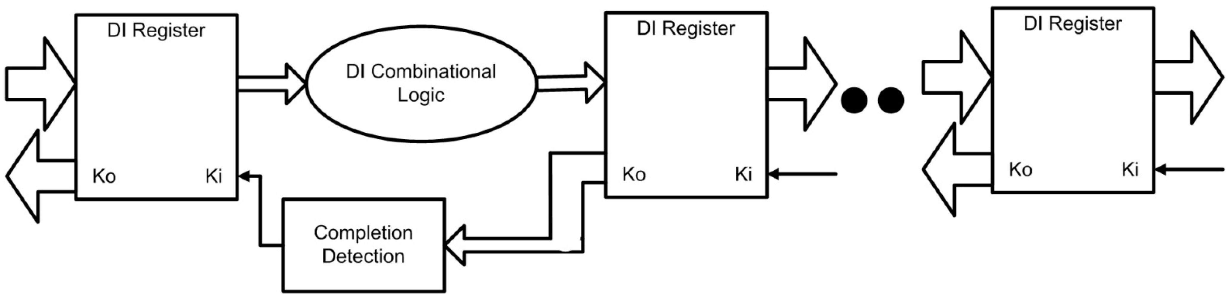
i.e., they are correct by construction), and also yield average-case performance rather than the worst-case performance of bounded-delay and traditional synchronous paradigms. Each data unit in a delay-insensitive system can take at least three values: DATA0, DATA1, and a spacer, also referred to as NULL. Delay-insensitive circuits communicate using request and acknowledge signals,
Ki and
Ko, respectively, as shown in the
Figure 1, to prevent the current DATA wavefront from overwriting the previous DATA wavefront, by ensuring that the two DATA wavefronts are always separated by a NULL wavefront. The acknowledge signal from the receiving circuit is the request signal to the sending circuit. When the receiver circuit latches the input DATA, the corresponding
Ko signal will become logic 0, indicating a request-for-NULL (
rfn); and when it latches the input NULL, the corresponding
Ko signal will become logic 1, indicating a request-for-DATA (
rfd). When the sending circuit receives a
rfd/
rfn on its
Ki input, it will allow a DATA/NULL wavefront to be output. This handshaking protocol coordinates DI circuit behavior, analogous to coordination of synchronous circuits by a clock signal. Additionally, delay-insensitivity requires the circuit to be input-complete, which means that all outputs may not transition from NULL to DATA until all inputs have transitioned from NULL to DATA, and that all outputs may not transition from DATA to NULL until all inputs have transitioned from DATA to NULL [
8].
Figure 1.
DI system framework: local handshaking instead of global clock control.
Figure 1.
DI system framework: local handshaking instead of global clock control.
NCL and PCHB DI circuit methods utilize at least two binary rail signals to represent a single bit of data. Hence, at least 2N wires are needed to represent N bits. Each of these rails requires its own set of gates to evaluate computations; therefore, dual-rail circuits typically require 1.5× to 2× transistors compared to Boolean logic. In this paper, a new method called Delay-Insensitive Ternary Logic (DITL) is detailed, which combines the design aspects of NCL, PCHB, and Boolean logic to form a delay-insensitive paradigm that only utilizes a single wire to represent a single bit of data, which has three distinct voltage levels corresponding to the three DI values of DATA0, DATA1, and NULL. Some advantages envisioned for DITL compared to NCL are half the number of interconnects, fewer transistors, and less power dissipation due to a reduced voltage swing for each NULL to DATA transition.
The paper is organized into the following sections.
Section 2 discusses an introduction to asynchronous paradigms, including NCL and PCHB, and also discusses previous work regarding ternary logic circuits.
Section 3 discusses the development of DITL at the gate-level using the example of a DITL NAND2 gate. A 1.2 V 130 nm IBM 8RF-DM CMOS process is used to design and simulate the DITL, NCL, and PCHB NAND2 circuits at the transistor-level; and a comparison of results is presented.
Section 4 discusses a secure hardware application for DITL and elaborates on the design methodology to create secure DITL circuits resistant to side-channel attacks utilizing timing, power, and electromagnetic emission measurements. A secure DITL Full Adder is designed and compared to NCL and Boolean methods for resistance to side-channel attacks. The developed DITL methodology is then utilized to design and simulate a physical-level implementation of a secure 8051 ALU, showing that the method can be scaled up to much larger circuits.
Section 5 concludes the paper.
2. Previous Work on Asynchronous and Ternary Logic
2.1. NULL Convention Logic (NCL)
NCL uses dual-rail signals to achieve delay-insensitive behavior. A dual-rail signal, D, consists of two wires, D0 and D1, which may assume any value from the set {DATA0, DATA1, NULL}. The DATA0 state (D0 = 1, D1 = 0) corresponds to a Boolean logic 0, the DATA1 state (D0 = 0, D1 = 1) corresponds to a Boolean logic 1, and the NULL state (D0 = 0, D1 = 0) corresponds to the empty set meaning that the value of D is not yet available. The two rails are mutually exclusive, so that both rails can never be asserted simultaneously; this state is an illegal state.
NCL utilizes threshold gates with hysteresis for its basic logic elements [
9]. The primary type of NCL gate is the THmn threshold gate, where 1
≤ m ≤ n, as depicted in
Figure 2. THmn gates have
n inputs and a threshold value of
m. At least m of the n inputs must be asserted before the output will become asserted. Because NCL gates are designed with hysteresis, all inputs must be de-asserted before the output will be de-asserted. This ensures a complete transition of inputs back to NULL before asserting the output associated with the next wavefront of input DATA. Therefore, a THnn gate is equivalent to an n-input C-element, and a TH1n gate is equivalent to an n-input OR gate. In the representation of a THmn gate, each of the
n inputs is connected to the rounded portion of the gate; the output emanates from the pointed end of the gate; and the gate’s threshold value,
m, is written inside of the gate.
Figure 2.
NCL threshold gate representation.
Figure 2.
NCL threshold gate representation.
For example, a TH23 gate has three inputs with a threshold value of two. Hence, the output is asserted when at least two of the three inputs are asserted. The output is then de-asserted only when all three inputs are de-asserted. A TH22 gate has two inputs and a threshold of two, such that the output is asserted/de-asserted only when both inputs are asserted/de-asserted. By employing threshold gates for each logic rail, NCL is able to determine the output status without referencing time.
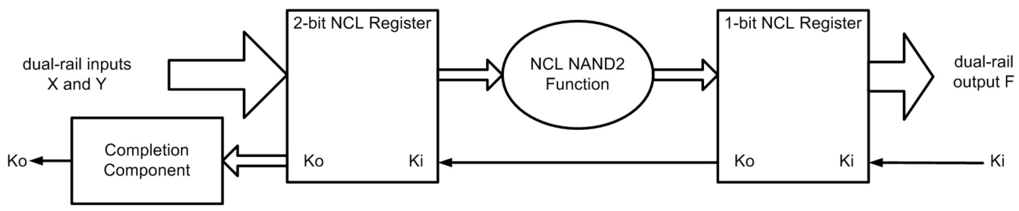
Figure 3 shows the design of a simple NCL system, consisting of two input NCL registers, followed by a NCL NAND2 function, and a single NCL register for the output.
Figure 3.
Simple NCL system for a NAND2 function.
Figure 3.
Simple NCL system for a NAND2 function.
The Completion Component is a TH22 gate used to combine the two
Ko signals from the input registers to create a single
Ko handshake output for the system. The internal design of NCL gates at the transistor-level, as well as the gate-level design of NCL components, such as an NCL Register, Completion Component, and NAND2 function, are detailed in [
8].
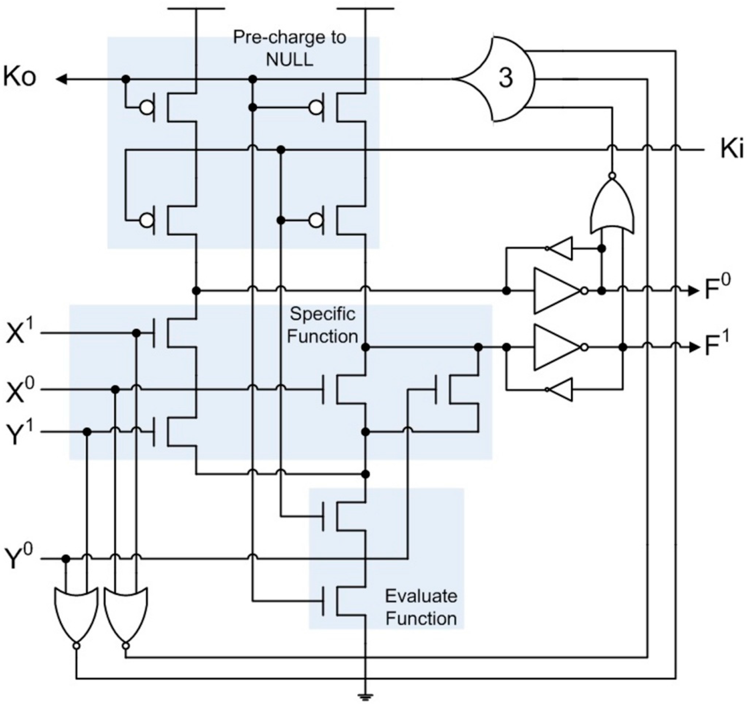
2.2. Pre-Charge Half-Buffer (PCHB)
PCHB circuits [
6] are designed at the transistor-level, utilizing dynamic CMOS logic, instead of targeting a predefined set of gates like in NCL. PCHB circuits have dual-rail data inputs and outputs, and combine combinational logic and registration together into a single block, as shown in
Figure 4, yielding a very fine-grain pipelined architecture.
Figure 4.
PCHB NAND2 circuit.
Figure 4.
PCHB NAND2 circuit.
The dual-rail output is initially pre-charged to NULL. When Ki and Ko are rfd, the specific function will evaluate when the inputs, X and/or Y, become DATA, causing the output, F, to become DATA. Ko will then transition to rfn only after all inputs and the output are DATA. When Ki is rfn and Ko is rfd, or vice versa, the output will be floating, so weak inverters must be used to hold the current output value. After both Ki and Ko are rfn, the output will be pre-charged back to NULL. After all inputs become NULL and the output changes to NULL, Ko will change back to rfd, and the next DATA wavefront can evaluate after Ki becomes rfd. PCHB circuits contain Boolean NOR2 gates, strong-weak inverter pairs, and a Th33 gate, which ensures that all data inputs and outputs are in the same state (either DATA or NULL) before toggling the Ko signal to request the next DATA or NULL wavefront.
2.3. Ternary Logic
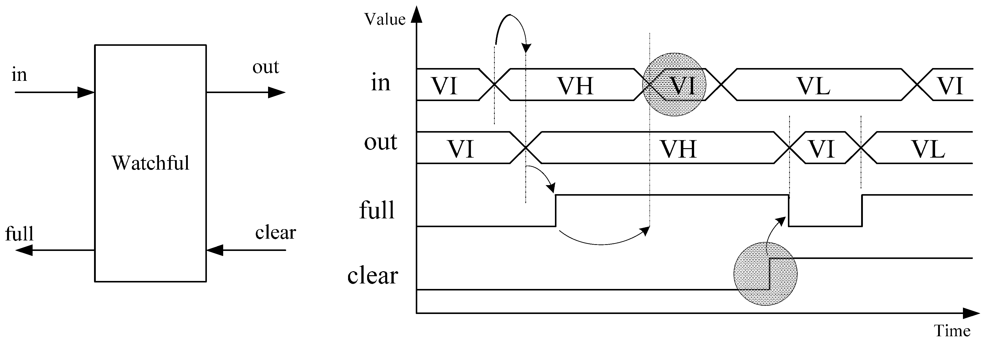
Ternary logic utilizes three distinct voltage values per wire, Vdd, ½ Vdd, and Gnd, whereas binary logic only utilizes two distinct voltage values, Vdd and Gnd. Hence, ternary logic can be used as an alternative to dual-rail logic to represent the needed three DI logic states (i.e., DATA0, DATA1, and NULL), requiring only one wire per bit. Vdd is used to represent DATA1, Gnd to represent DATA0, and ½ Vdd to represent NULL, which yields maximum noise margin with minimum switching power dissipation, since each wire always switches to NULL between every two DATA states, such that the voltage swing is always ½ Vdd.
References [
10,
11] develop a ternary logic completion detection circuit for use with a bounded-delay self-timed paradigm; and references [
12,
13] develop a ternary bounded-delay self-timed paradigm, which is similar to micropipelines [
4]. However, as mentioned in the introduction, delay-insensitive paradigms have many more advantages compared to their bounded-delay counterparts. Reference [
14] develops a delay-insensitive ternary logic transmission system, called Asynchronous Ternary Logic Signaling (ATLS), which converts dual-rail signals into ternary logic for transmission over a bus, in order to decrease transmission area and power. However, all of the logic processing is still done using dual-rail logic. References [
15,
16] develop a circuit called a
Watchful as part of their proposed delay-insensitive ternary logic paradigm. However, their approach is not delay-insensitive because it assumes that the input,
in, will transition to
VI (NULL) before the input,
clear, is asserted, causing the output,
full, to be de-asserted, shown by two shaded circles in the adapted timing diagram in
Figure 5.
Figure 5.
Watchful timing diagram adopted from [
15,
16].
Figure 5.
Watchful timing diagram adopted from [
15,
16].
In order to become delay-insensitive, full must not be de-asserted until both clear is asserted and in transitions to VI. Otherwise, if in remained at a single DATA value (e.g., if no additional data needs to be processed at that time), this DATA value would continue to be utilized in subsequent operations instead of causing the system to become idle.
Reference [
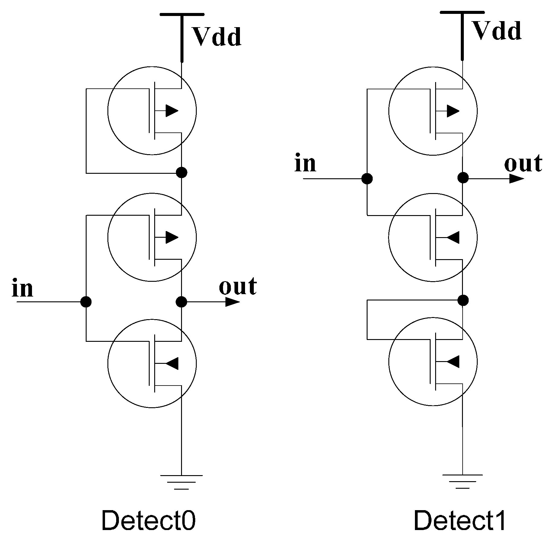
17] utilizes diode-connected transistors to shift the threshold voltage in special inverters dedicated to detect the presence of only one input logic level. As shown in
Figure 6, for the Detect0 circuit,
in, must be lower than Vdd-2Vt
P for the PMOS transistors to turn ON and pull
out to Vdd. Similarly, for the Detect1 circuit,
in, must be higher than 2Vt
N for
out to be pulled down to Gnd. The truth table for Detect0 and Detect1 is provided in
Table 1.
Figure 6.
Original ternary logic Detect circuits adapted from [
17].
Figure 6.
Original ternary logic Detect circuits adapted from [
17].
Table 1.
Truth Table for Detect Circuits.
Table 1.
Truth Table for Detect Circuits.
| Ternary Input | Detect0 | Detect1 |
|---|
| DATA0 (Gnd) | 1 | 1 |
| NULL (½ Vdd) | 0 | 1 |
| DATA1 (Vdd) | 0 | 0 |
3. Delay Insensitive Ternary Logic (DITL)
Delay-Insensitive Ternary Logic (DITL) is a new paradigm that utilizes three distinct voltage levels, i.e., Vdd, ½ Vdd, and Gnd, to encode the three delay-insensitive logic states, DATA1, NULL, and DATA0, respectively, on a single wire. The motivations for utilizing ternary logic for delay-insensitive circuit design include reducing area (only half the number of wires are required for each bit compared to dual-rail logic) and reducing power/energy (each transition, NULL to DATA or vice-versa, only requires a ½ Vdd swing compared to a full Vdd swing for dual-rail logic). DITL utilizes DI request and acknowledge signaling to move DATA and NULL wavefronts from one stage to the next without a clock. Like PCHB, DITL circuits are designed at the transistor-level, incorporate registration and combinational logic into a single component, and pre-charge the internal node to NULL before each function evaluation. DITL has ternary logic inputs and outputs and binary logic handshaking signals. DITL utilizes Boolean logic, consisting of DATA0 and DATA1, to implement a specific component, such as a 2-input NAND gate, since the 3rd logic level, ½ Vdd, is only used as the NULL state that separates every two adjacent DATA states.
3.1. Distinguishing Ternary Logic States
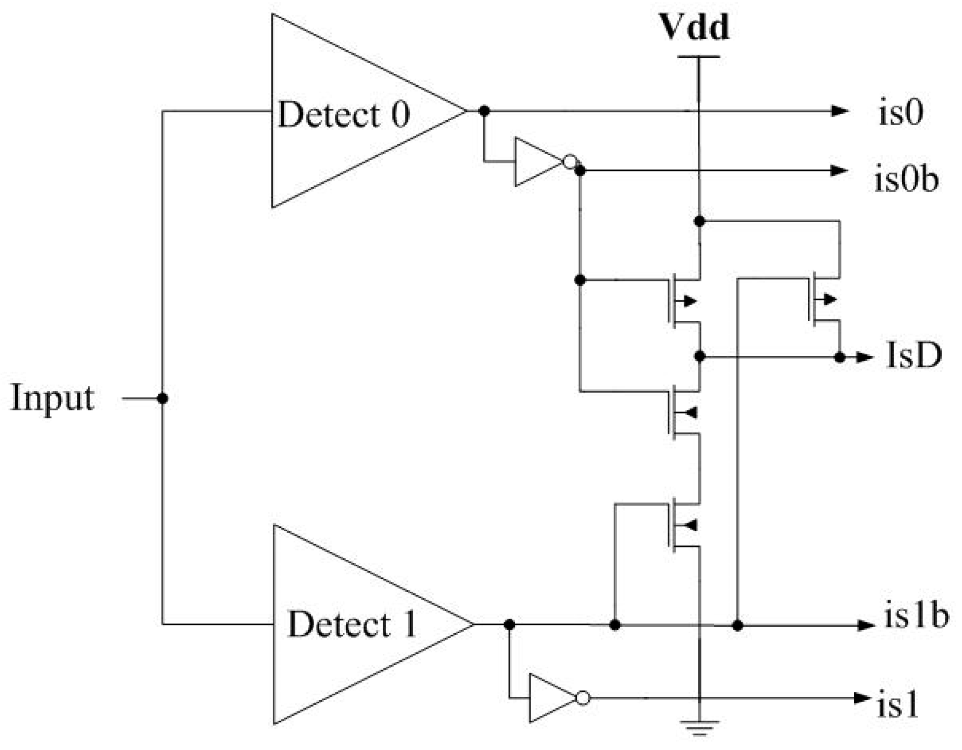
DITL distinguishes between ternary logic states of DATA0, DATA1, and NULL using the Is-DATA component shown in
Figure 7. Is-DATA asserts the primary output
IsD when the ternary signal,
Input, is either DATA1 or DATA0, and de-asserts the output when Input is NULL. The truth table for Is-DATA is given in
Table 2. The Is-DATA component utilizes Detect0 and Detect1 circuits. Using the 1.2 V 130 nm IBM 8RF-DM process, the original detect circuits discussed in
Section 2.3 were simulated at the transistor-level and were found to consume significant static power because all transistors are partially turned ON for a NULL (½ Vdd) input, yielding 31.8 nW for Detect0 and 5.5 nW for Detect1. Additionally, they require extra inverters to properly shape the outputs; otherwise the output is only 1.07 V instead of 1.2 V for Detect0 with an input of 0 V, and 0.17 V instead of 0 V for Detect1 with an input of 1.2 V. To decrease static power consumption, a method called Reverse Body Bias (RBB) [
18,
19,
20] was used. In RBB, a voltage higher than Vdd is applied as the PFET body bias and a voltage lower than Gnd is applied as the NFET body bias so as to increase the threshold voltage, which results in less leakage and static power. The maximum steady state voltage allowed between any two terminals (gate, source, drain, and body) of a FET cannot exceed Vddmax, which is 1.6 V for this 1.2 V 130 nm process. Hence, the original detect circuits were modified with all PFET body biases set to 1.6 V and NFET body biases to −0.4 V, as shown in
Figure 8. This resulted in a Detect0 with steady state power of 8nW and propagation delay of 0.55 ns; and a Detect1 with 0.75 nW and 0.65 ns.
Figure 7.
Is-DATA component.
Figure 7.
Is-DATA component.
Figure 8.
Modified ternary logic detect circuits with RBB.
Figure 8.
Modified ternary logic detect circuits with RBB.
Table 2.
Truth Table for Is-Data component.
Table 2.
Truth Table for Is-Data component.
| Ternary Input | IsD | is1 | is0 |
|---|
| DATA0 (Gnd) | 1 | 0 | 1 |
| NULL (½ Vdd) | 0 | 0 | 0 |
| DATA1 (Vdd) | 1 | 1 | 0 |
Figure 9.
DITL Version I NAND2 component: data inputs X and Y are directly connected to the Specific Function block.
Figure 9.
DITL Version I NAND2 component: data inputs X and Y are directly connected to the Specific Function block.
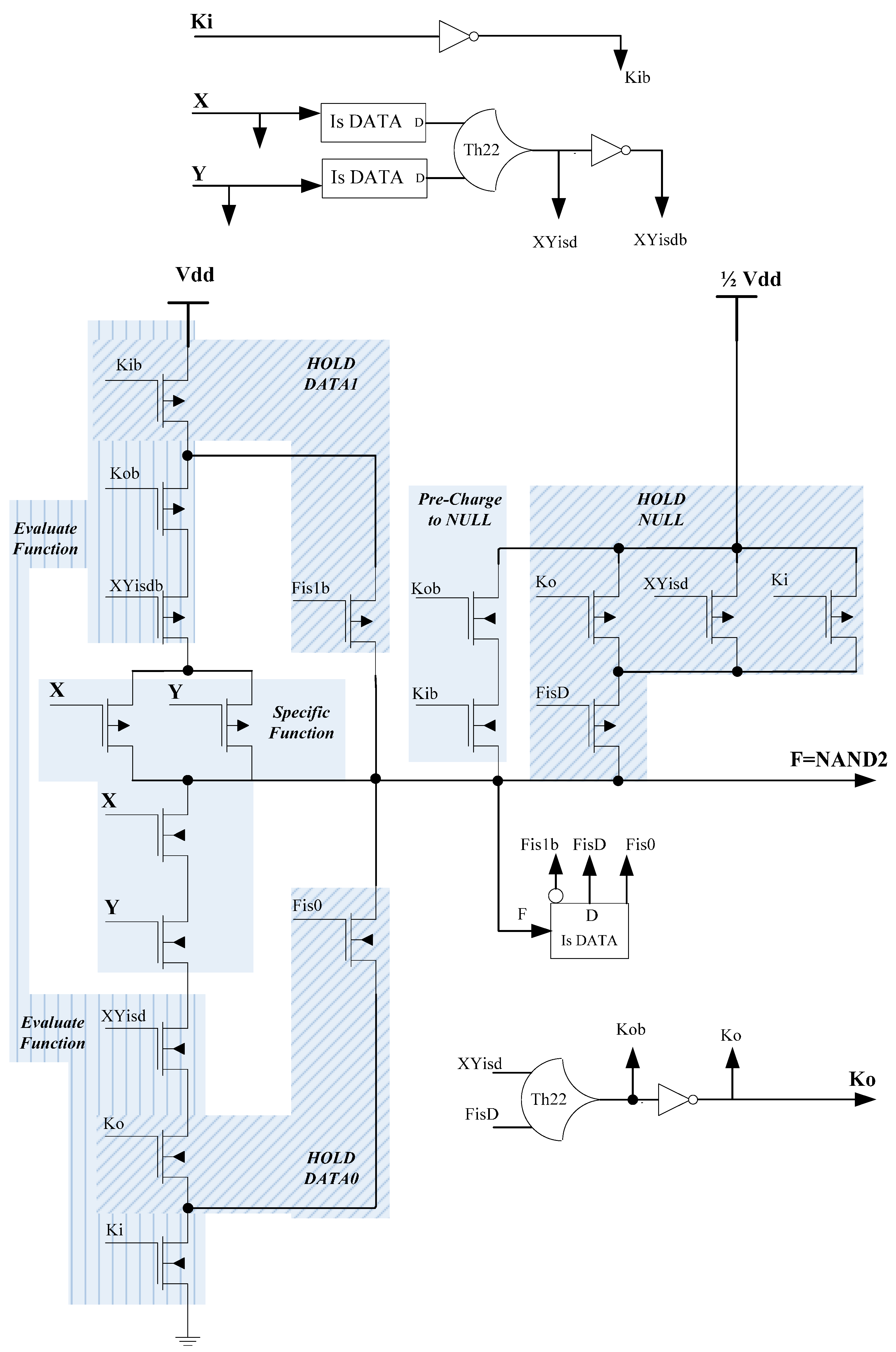
3.2. DITL Architecture
Like PCHB, DITL circuits are designed at the transistor-level, with registration included in every combinational logic component; the major difference is that DITL uses ternary data inputs and outputs, while PCHB utilizes binary dual-rail inputs and outputs. Two different versions of the DITL architecture are presented herein. For DITL Version I, shown in
Figure 9, data inputs
X and
Y are directly connected to the Is-DATA components as well as the Specific Function. When
Ki and
Ko are both
rfd and the inputs,
X and
Y, are both DATA, the specific function will evaluate, causing the output,
F, to become DATA, which will then transition
Ko to
rfn. When
Ko is
rfn and
Ki is still
rfd, the specific function is floating, so the output needs to be held at its proper DATA value, either DATA0 or DATA1, which is done through the Hold 0 and Hold 1 circuitry, respectively. After
Ki changes to
rfn, the output will be pre-charged to NULL (
i.e., ½ Vdd), through NFETs for increased speed. After all inputs become NULL and the output changes to NULL,
Ko will change back to
rfd, and the next DATA wavefront can evaluate after
Ki becomes
rfd and the inputs change to DATA. If
Ki changes to
rfd before the inputs become NULL, if the inputs become NULL before
Ki changes to
rfd, or if both
Ki and
Ko are
rfd but the inputs are still NULL, the pre-charge to NULL logic will no longer be conducting, so the NULL output must be maintained through the Hold NULL circuitry.
Figure 10 shows the Cadence simulation of the DITL NAND2 circuit, using the same IBM process. As can be seen from the waveforms, output
F transitions to DATA only when both
Ki (Lack) and
Ko (Rack) are
rfd and both inputs,
X and
Y, are DATA.
F can transition back to NULL as soon as both
Ko and
Ki are
rfn.
Figure 10.
Cadence simulation of DITL NAND2 component.
Figure 10.
Cadence simulation of DITL NAND2 component.
Version II of the DITL architecture is shown in
Figure 11, where the Specific Function inputs come from the input Is-DATA components instead of the external inputs,
X and
Y. Version II requires one additional inverter inside the Is-DATA component for the
is1 output corresponding to each data input, but the advantage is that each data input drives exactly one Is-DATA component for each DITL circuit to which it is an input, such that the capacitance driven by a particular signal only depends on the number of circuits to which the signal is an input, and not on the type of circuits it drives For example, if signal
A is an input to an XOR2 and NOR3 circuit, and signal
B is an input to a NAND4 and OR2 circuit, both drive the same amount of capacitance because they both drive two Is-DATA components. The use of Version II DITL circuits in a secure hardware application is discussed in detail in
Section 4.
Figure 11.
DITL Version II NAND2 component: data inputs X and Y are connected only to the input Is-DATA components.
Figure 11.
DITL Version II NAND2 component: data inputs X and Y are connected only to the input Is-DATA components.
3.3. Comparing DITL with PCHB and NCL
The NAND2 circuits previously discussed,
i.e., NCL in
Figure 3, PCHB in
Figure 4, and DITL in
Figure 9 and
Figure 11, were simulated in Cadence and the results are listed in
Table 3. DITL Version I is slightly slower, but requires slightly less area and energy compared to Version II. Compared to PCHB, DITL is 21% slower, 74% larger, but requires 68% less energy. Compared to NCL, DITL is 50% slower, but requires 38% less energy and is 89% smaller. Therefore, DITL has a significant energy advantage compared to PCHB and NCL, and is also more area efficient than NCL. Additionally, as circuit size increases, DITL and PCHB circuits increase at a much smaller rate than NCL circuits (e.g., for a NAND2
vs. a NAND4 circuit, the area increase is 42% for DITL, 70% for PCHB, and 94% for NCL). Comparing average static power, DITL consumes 140% more than PCHB and 13% more than NCL. DITL peak dynamic power is 13% less than NCL and 81% more than PCHB.
Table 3.
Nand2 comparison: DITL vs. PCHB vs. NCL.
Table 3.
Nand2 comparison: DITL vs. PCHB vs. NCL.
| Type of Design | Avg. DATA-NULL Cycle (ns) | Avg. Energy per Operation (fJ) | Area (# of Transistors) | Avg. Static Power (nW) | Max. Dynamic Power (uW) |
|---|
| DITL V1 | 5.43 | 50.3 | 78 | 6.9 | 60 |
| DITL V2 | 5.40 | 52.3 | 82 | 7.5 | 67 |
| PCHB | 4.49 | 86.3 | 46 | 3 | 35 |
| NCL | 3.61 | 70.8 | 151 | 6.35 | 72 |
4. DITL Secure Hardware Application
The increasingly pervasive use of digital information storage and processing devices largely facilitates societal activities, ranging from people’s everyday life to government and military missions. The demands of storing and processing sensitive information, e.g., passwords, messages, personnel records, have resulted in incorporating strong cryptographic algorithms inside these devices. Sensitive information is first encrypted by the host device and becomes cipher text before it is transferred to another device, where the cipher text is decrypted into plaintext for processing. Since most pervasive data storage and processing devices use one or more Integrated Circuits (ICs) as a core component(s), incorporating cryptography on-chip significantly enhances the security of the information being stored/processed due to the fact that modern cryptographic algorithms, e.g., Advanced Encryption Standard (AES), Rivest-Shamir-Adleman (RSA), are very difficult to break in a brute-force way. However, attackers have switched their targets from the cryptographic algorithms themselves to the implementations of these algorithms. In particular, attackers have been able to exploit on-chip security information, e.g., cryptographic keys, through “side-channel” measurements, including power consumption, timing, and electromagnetic (EM) emissions.
From a hardware perspective, such side-channel attacks can be implemented at both the circuit- and architecture-level. At the circuit-level, due to CMOS circuit characteristics, a digital CMOS IC exhibits fluctuations in side-channel measurements of timing, power, and EM emissions while processing different data, causing information leakage. By applying statistical algorithms to the measured transient side-channel data, attackers are able to decipher the secure information stored on-chip. This paper discusses circuit-level side-channel attack mitigation using DITL. As proof of concept, a series of full adders were designed in Boolean, NCL, and DITL at the transistor-level, using the IBM 8RF-DM 0.13 µm process and compared for different power and timing parameters, showing that DITL is the best option for designing secure functional units. Afterward, a DITL library for secure gates was created and a DITL ALU circuit employing these gates was designed and simulated.
Physical/invasive attacks are excluded in this research. Such attacks require de-packaging the target IC to expose the internal die, and using special equipment to monitor/modify circuit elements or stored data. Examples include micro-probing attacks, chip rewriting attacks, and memory remanence attacks. There are two reasons for making this assumption: (1) such attacks require special equipment, a much longer time, and highly skilled attackers to perform, which significantly limits the number of ICs/applications that require this type of protection; and (2) a number of physical and even destructive protection mechanisms have been developed, such as inserting pressure sensors on-chip to sense de-packaging behaviors. If needed, these mechanisms can be included with the secure chip to achieve an even higher level of security.
4.1. Problems of Existing Security Solutions
Much research has been performed in mitigating side-channel attacks, and a number of solutions have been proposed. Unfortunately, these solutions have one or more weaknesses/limitations, as discussed below.
4.1.1. Inflexibility
Most solutions are developed to protect a single cryptographic algorithm (e.g., AES, RSA) in mitigating one or two side-channel attacks (e.g., power, timing). Therefore, the flexibility of these solutions is severely limited. This inflexibility is two-fold: (1) there is no universal solution to all four major categories of side-channel attacks, i.e., power-, timing-, EM-, and fault-based attacks; and (2) there is a lack of general side-channel mitigation techniques that can be adopted by all prevailing cryptographic algorithms, such that when the user switches to another algorithm, there will be no major changes in the hardware design methodology for increased security.
4.1.2. High Overhead
Almost all existing solutions add significant overhead to the original implementation. Such overhead includes higher power consumption, longer processing delay, larger chip area, reduced circuit reliability, higher design complexity, and incompatibility with the commercial digital IC design flow. For example, dual-rail asynchronous logic for mitigating power-based attacks causes considerable timing and area overhead and requires a customized design flow; various pre-charge based dynamic logic paradigms introduce additional power consumption, increased design complexity, and reliability degradation; fault-tolerant techniques usually incur severe penalties in power, timing, and area. Such overhead hinders the wide adoption of these side-channel attack countermeasures in commercial products.
4.2. Common Circuit Level Side-Channel Attack Methods and Countermeasures
4.2.1. Power-Based Attacks
Most electronic devices running cryptographic algorithms are implemented in CMOS technology, where transistors act as voltage-controlled switches. While a circuit node is switching, electrons flow across the corresponding transistors to charge/discharge its load capacitance, thereby consuming power. Due to the fact that different transistors will be turned ON/OFF while processing different data, causing different power consumption, side-channel attacks in this category are implemented using the IC’s transient power data. The theory of power-based attacks, e.g., Differential Power Analysis (DPA), was introduced in [
21,
22]. In general, these attacks require the transient power data while the target IC performs encryption/decryption on different texts, and then use statistical algorithms to derive the key. Power-based attacks are the most powerful and prevalently implemented side-channel attacks, which have been successfully implemented to crack almost all cryptographic algorithms on different platforms, including Data Encryption Standard (DES) [
23], Elliptic Curve Cryptosystems [
24], RSA [
25,
26], AES [
27,
28], and all AES candidates [
29], implemented on FPGAs [
30] and as ASICs [
27].
A number of methods have been proposed for mitigating power-based attacks by decoupling transient power consumption from the data being processed. Techniques based on balancing power fluctuation include new CMOS logic gates [
31,
32,
33,
34,
35,
36,
37,
38,
39,
40,
41,
42,
43,
44,
45,
46], which go through a full charge/discharge cycle for each data processed. Asynchronous circuits, especially dual-rail encoded logic, have been well studied for anti-DPA because of the fixed switching activities during each DATA-Spacer cycle [
47,
48,
49,
50,
51,
52,
53,
54,
55,
56,
57,
58,
59,
60,
61,
62,
63,
64,
65]. Other power balancing methods include modifying the algorithm execution [
66,
67,
68,
69], compensating current at the power supply node [
70,
71,
72,
73], and using subthreshold operation [
74]. Additionally, many techniques for randomizing power data have been proposed [
75,
76,
77,
78,
79,
80,
81,
82,
83,
84,
85,
86].
4.2.2. Timing-Based Attacks
The principle of timing-based attacks is very similar to power-based ones except these attacks rely on timing fluctuations of the target circuit while processing different data patterns. Depending on the load capacitance and driving strength, the charge/discharge process during the switching activities at an internal circuit node will take different amounts of time to finish, which in turn causes different timing delays. First introduced in [
87], Timing Analysis (TA) attacks have demonstrated their success on RSA [
88], DES [
89], AES [
90], RSA with Montgomery multiplications [
91], and GPS systems [
92]. Existing countermeasures include inserting dummy operations [
93], using redundant representation [
94], and unifying the multiplication operands [
95].
4.2.3. Electromagnetic-Based Attacks
Due to the inevitable existence of parasitic reactance, electrical current flowing through a switching CMOS gate causes a variation in the EM field surrounding the chip, which can be monitored by antennas particularly sensitive to the related impulse [
96]. Similar statistical analysis methods can be applied utilizing EM variances while the target chip is processing different data. Simple and Differential Electromagnetic Attacks (SEMA and DEMA) have been successfully implemented to crack DES [
97,
98], (Rivest Cipher 4) RC4 [
99], AES [
100], and Ellipse Curve Cryptosystems [
96,
101], on both FPGAs [
96,
101] and Smart-Cards [
102]. Although some power-balancing methods also reduce EM fluctuations, masking EM variance is more complex due to increased difficulty in matching parasitic reactance. EM attack countermeasures include signal strength reduction and signal information reduction [
98].
4.2.4. Fault-Based Attacks
Unlike the previous three passive attacks, fault-based attacks are semi-active in that attackers need to perform certain unusual operations to induce faults inside the target circuit. During the existence of faults, the circuit outputs as well as the side-channel information will be monitored and Differential Fault Analysis (DFA) will be applied to perform the attack, the effectiveness of which has been demonstrated on DES [
103], RSA [
104,
105,
106,
107,
108], Ellipse Curve Cryptosystems [
109,
110,
111], AES [
112,
113,
114,
115,
116], Common Scrambling Algorithm [
117,
118], and RC4 [
119].
Fault-injection methods can be classified as non-invasive (variations in supply voltage, external clock, and/or temperature), semi-invasive (exposure to white light, lasers, X-rays, and EM fields), and invasive (ion beams, active probes, and circuit modification) [
120]. In general, most fault-tolerant design techniques, such as temporal and spatial redundancy, can be applied to mitigate certain types of faults. These techniques include Concurrent Error Detection (CED) [
121,
122,
123,
124,
125,
126,
127,
128,
129,
130], error detection/correction code [
131,
132,
133,
134,
135,
136,
137,
138,
139,
140,
141,
142,
143], modular redundancy [
144,
145], Built-In Self-Test (BIST) [
146], and algorithm modification [
147,
148,
149,
150,
151,
152,
153]. In addition, the use of dual-rail encoding and its fault analysis can be found in [
130,
154,
155,
156].
4.3. Circuit-Level Side-Channel Attack Mitigation Using DITL
Most DI paradigms [
5,
157,
158,
159,
160,
161,
162] utilize multi-rail signals, such as dual-rail logic, to achieve delay-insensitivity. For DI methods, separating two adjacent DATA wavefronts by a NULL wavefront [
163] guarantees that there are always two switching events for each dual-rail signal for every DATA processed, thereby decoupling the total number of switching events from the data being processed. However, as pointed out in reference [
164], the imbalanced load between the two rails still causes considerable power/timing/EM fluctuations among different data patterns.
At the circuit-level, DITL is utilized for designing logic circuits with properly sized transistors. While maintaining the advantages of asynchronous logic in mitigating side-channel attacks, e.g., distributed and balanced switching activities, DITL eliminates the drawbacks such as average performance that facilitates timing-based attacks, and the imbalanced load capacitance between the two rails. Using the single wire per bit DITL methodology at the circuit-level has the advantage that power, timing, and emissions can be more easily balanced to prevent attacks compared to dual-rail delay-insensitive methods. In addition, DITL offers a number of other benefits including lower power, higher performance, and commercial design flow compatibility.
Since DITL circuits only have a single output wire per bit, timing, power, and EM can be more easily balanced because each signal will only drive a single capacitance, as in the case of the DITL Version II architecture discussed earlier (
Figure 11); and a gate’s output will always make a ½ Vdd transition every DATA and NULL cycle, regardless of the DATA value (
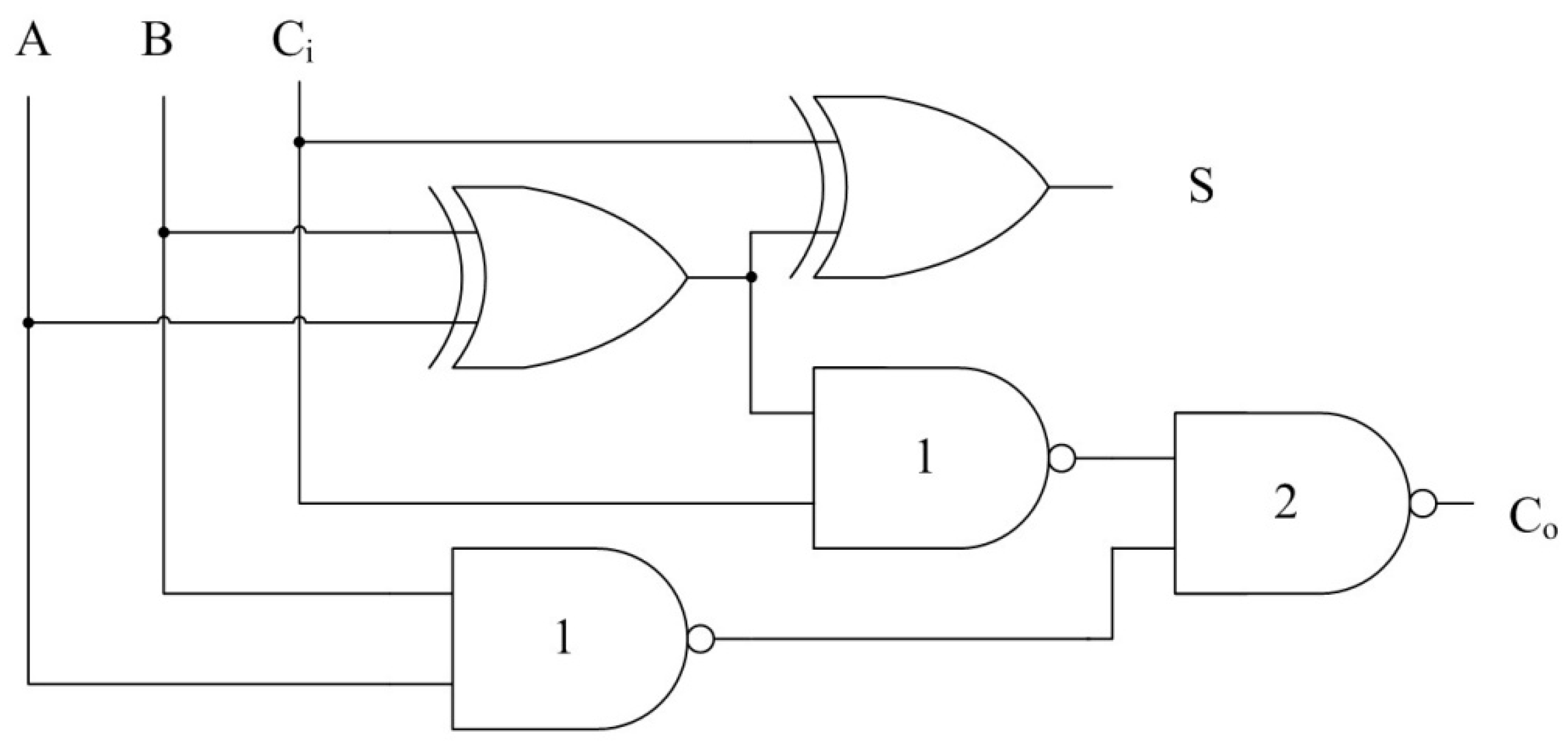
i.e., ½ Vdd → Vdd → ½ Vdd for a N→D1→N transition and ½ Vdd → 0 → ½ Vdd for a N→D0→N transition). Since each DITL Version II gate input always drives exactly one Is-DATA component, the type of gate being driven will not affect the load capacitance, such that the output driving strength selection of a DITL gate only depends on the number of gates it drives, which substantially reduces the number of balanced gates needed for a chip design library. As proof of concept, a series of Full Adders (FAs) was designed in Boolean, NCL, and DITL, using the same IBM process. The Boolean FA is a standard gate-level design consisting of five logic gates, as shown in
Figure 12.
Figure 12.
Five gate Full Adder for Secure DITL and Boolean Logic.
Figure 12.
Five gate Full Adder for Secure DITL and Boolean Logic.
For the NCL FA, two versions have been designed: one is a 10-gate design based on utilizing complete logic functions to directly implement
Figure 12, denoted as NCL-10G; the other is an optimized four-gate design [
9], denoted as NCL-4G. Being compatible with its Boolean counterpart, the DITL FA also consists of five gates with different driving strengths, balanced for timing/power through proper transistor sizing. To balance timing and power, transistors were sized to yield similar output→DATA and output→NULL times, propagation delays, peak current spike during transitions, and energy, for all possible transitions. Note that the first two NAND2 gates in
Figure 12, denoted by “1”, are sized with driving strength of one gate, while the last NAND2 gate, denoted by “2”, has a driving strength of two gates, since it will be used to drive the
Cin input of a subsequent FA, connected in ripple-carry fashion. Simulations of balanced DITL NAND2(1), NAND2(2), and XOR2 gates yielded the results shown in
Table 4. Explaining the case of one of the DITL gates in
Table 4, the output→DATA0/1 times were made to be as close as possible to each other when all of the four input patterns possible for the two-input gate were applied to the gate. This requires appropriately sizing and balancing the PFET network that sets the output to DATA1 and the NFET network that resets the output to DATA0 in the DITL Version II architecture depicted in
Figure 11. Likewise, the output→NULL times were made similar to each other over all four input patterns by sizing and balancing the network for ½ Vdd. It was found that using pass transistor gates instead of two NFETs in series to channel ½ Vdd was best suited to yield better balanced times.
The energy over an entire operation, where each NULL→DATA0/1→NULL is a single operation, was made to be as close as possible to each other over all four possible operations. To do this without changing the time balanced transistors of the DITL gate pull up and pull down networks, extra inverter like small circuits were introduced to selectively dissipate power. These circuits are controlled by outputs of the Is-DATA component, such that these circuits turn ON to dissipate power for some selected input patterns while not serving any logical function. The final result is that all input patterns produce almost the same energy consumption for the DITL gate over an entire operation. To match peak current spikes for each operation, extra inverters that serve no logical function are added that turn ON for selected input patterns to create a similar reading for every input pattern. In short, for
Table 4, all values that appear in a single row need to be as close as possible to each other, so the individual balanced DITL gates were designed to achieve this.
Table 4.
Measurements from balanced DITL gates.
Table 4.
Measurements from balanced DITL gates.
| Input Pattern | NULL→ 00→ NULL | NULL→ 01→ NULL | NULL→10→ NULL | NULL→ 11→ NULL |
|---|
| DITL Nand2 (1) | Output → DATA (ps) | 519.9 | 546.1 | 529.5 | 537.6 |
| Output → NULL (ps) | 565.5 | 574.5 | 552.5 | 582.7 |
| Energy (fJ) | 36.3 | 37.6 | 37.5 | 36.3 |
| Current Spike (uA) | 55 | 54 | 55 | 56 |
| DITL Nand2 (2) | Output → DATA (ps) | 659.5 | 691.4 | 670.7 | 671 |
| Output → NULL (ps) | 682.2 | 678 | 660.2 | 653.4 |
| Energy (fJ) | 38.4 | 39.4 | 39.3 | 39.2 |
| Current Spike (uA) | 55 | 54 | 54 | 58 |
| DITL Xor2 | Output → DATA (ps) | 783.9 | 780.7 | 779.7 | 774.9 |
| Output → NULL (ps) | 636.8 | 617.6 | 625.5 | 633.3 |
| Energy (fJ) | 44.6 | 44.1 | 44.2 | 44.5 |
| Current Spike (uA) | 71 | 58 | 59 | 58 |
After balancing the NAND2 and XOR2 gates, they were combined to form a five-gate balanced DITL FA. The simulations of the DITL FA yielded the results summarized in
Table 5. No further balancing or transistor sizing was done on the FA. In
Table 5, as expected, the values in a single row are very close to each other over all eight possible FA input patterns.
Table 6 shows the maximum variance percentage of each parameter among all possible input combinations, and compares the DITL FA to the NCL and Boolean full adders. These four FAs were simulated in Cadence Spectre and are compared in five categories: “
Sum/
Cout transition slope” is the combined rise/fall time during each transition for
Sum and
Cout outputs, respectively; “delay” is the total time for a N→D→N cycle; “peak current spike” is the magnitude of the supply voltage current spike during each transition; and “energy” is the total energy consumed during each transition.
Although NCL as a dual-rail asynchronous logic is well-known to be more side-channel attack resistant compared to Boolean logic, the DITL design exhibits the least variations in all parameters, as shown in
Table 6. Since power (energy and current spike) and timing (slope and delay) are significantly more balanced for DITL, DPA and TA will be much more difficult to succeed. This demonstrates DITL’s capability to balance power and timing with different driving strengths in a multi-gate circuit, which validates the balanced DITL cell library development strategy undertaken.
Table 5.
Measurements from Balanced DITL Full Adder.
Table 5.
Measurements from Balanced DITL Full Adder.
| Input Patterns from 0 to 3 | NULL→ 000→ NULL | NULL→ 001→ NULL | NULL → 010→ NULL | NULL → 011→ NULL |
| DITL FA Sum | Output → DATA (ps) | 645.1 | 665 | 665.8 | 665.4 |
| Output → NULL (ps) | 487.9 | 488.3 | 539.2 | 484.7 |
| DITL FA Carry | Output → DATA (ps) | 587.1 | 587.1 | 589.9 | 606.1 |
| Output → NULL (ps) | 562 | 566.2 | 562.4 | 606.1 |
| Energy (fJ) | 305 | 303 | 310 | 290 |
| Current Spike (uA) | 301 | 277 | 289 | 283 |
| Input Patterns from 4 to 7 | NULL → 100→ NULL | NULL → 101→ NULL | NULL → 110→ NULL | NULL → 111→ NULL |
| DITL FA Sum | Output → DATA (ps) | 677.9 | 657.8 | 636.7 | 665.8 |
| Output → NULL (ps) | 537.8 | 491.6 | 483.8 | 487.1 |
| DITL FA Carry | Output → DATA (ps) | 585.6 | 600 | 596.1 | 592.2 |
| Output → NULL (ps) | 557.1 | 605.5 | 601.5 | 602.3 |
| Energy (fJ) | 311 | 291 | 287 | 284 |
| Current Spike (uA) | 290 | 284 | 277 | 290 |
Table 6.
Secure Full Adder Comparison.
Table 6.
Secure Full Adder Comparison.
| Full Adder | Maximum Variance Percentage (%) |
|---|
| Sum Transition Slope | Cout Transition Slope | Delay | Peak Current Spike | Energy |
|---|
| Boolean | 27.8 | 11.4 | 93.6 | 221.4 | 313.4 |
| NCL-4G | 21.0 | 13.0 | 105.3 | 51.0 | 32.0 |
| NCL-10G | 12.9 | 58.4 | 19.0 | 47.2 | 10.4 |
| DITL | 8.5 | 5.6 | 13.8 | 18.1 | 7.4 |
4.4. DITL ALU Design and Simulation Results
Utilizing the methods to develop the DITL secure FA discussed in
Section 4.3, a DITL balanced gate library was created to be used to design a DITL Secure 8051 Arithmetic Logic Unit (ALU). The gate library consisted of timing and power balanced DITL circuits for Half Adder, Full Adder, 2:1 Multiplexers, two- to four-input versions of NAND and NOR gates, XOR2 and XNOR2 gates, and several inverters and buffers with a variety of drive strengths. The developed library also contained C-elements [
9] for use in the completion circuitry to conjoin multiple
Ko signals together and ternary buffer circuits to increase drive strength of ternary signals as needed. All the DITL gates were created at the transistor-level and simulated using the same IBM 1.2 V 130 nm 8RF-DM process, and then laid out. The Boolean 8051 ALU was first designed in VHDL. Then all of the Boolean gates were replaced by DITL equivalents with connections added for
Ko and
Ki handshaking signals.
The resulting DITL ALU netlist was imported into Cadence as a transistor-level design and simulated. The DITL ALU schematic is not included here as it is much too large to be legible; however,
Figure 13 shows the testbench used to simulate the design. It contains the symbol for the ALU and a VerilogA controller, which generates inputs to the ALU.
Figure 14 shows the Cadence Ultrasim simulation waveforms, which include the supply current, handshaking signals,
Rack (Ki) and
Lack (Ko), one of the many data inputs,
Tmp1bus<0>, and one of the many data outputs,
resultH<0>. It includes the simulation results for eight different DATA/NULL input patterns.
Figure 13.
DITL ALU testbench.
Figure 13.
DITL ALU testbench.
Figure 14.
DITL ALU Ultrasim simulation.
Figure 14.
DITL ALU Ultrasim simulation.
The ALU simulation was performed as follows: Simulation time was calculated for each DATA wavefront to produce an output DATA, and each NULL wavefront to produce an output NULL, for all different ALU operations using eight random data input patterns each, and then averaged to produce the average delay per DITL ALU operation, referred to as TDD or DATA-to-DATA cycle time. This TDD Delay was measured as 135 ns. Total energy was calculated by integrating the current waveform for both Vdd and ½ Vdd (not shown in
Figure 14, but similar to I(Vdd)) over the entire simulation time, and multiplying these by the respective supply voltages, 1.2 V and 0.6 V. These two total energies were then summed and averaged over the total number of operations to obtain energy per operation which was measured to be 0.178 nJ. The energy required from the ½ Vdd supply was negligible compared to that from Vdd. The static power readings during the times when all ALU outputs are either all DATA or all NULL and the circuit is not switching were found separately by obtaining the current values from the Vdd and ½ Vdd supplies between the different input patterns, averaging these, and multiplying by their respective supply voltages, 1.2 V and 0.6 V, then summing the two. Following this logic, the ALU static power while output is DATA was measured as 137 μW and while output is NULL was measured as 87.5 μW. After the transistor level simulation proved successful, a layout was created for the DITL ALU using Cadence Virtuoso, as shown in
Figure 15, which is ready to be integrated into a layout plan with pads and be taped out for fabrication.
Figure 15.
DITL ALU layout.
Figure 15.
DITL ALU layout.
5. Conclusions and Future Work
A new asynchronous logic paradigm called Delay-Insensitive Ternary Logic (DITL) was developed, which combines design aspects of NCL, PCHB, and Boolean logic. DITL uses a single wire per bit, three-voltage scheme to represent the three states needed for delay-insensitive signaling, i.e., DATA0, DATA1, and NULL. DITL was found to be more energy efficient when compared to similar paradigms, such as PCHB and NCL, when simulated using the IBM 8RF-DM 1.2 V 130 nm CMOS process. DITL was then applied to secure hardware design, showing that it is less susceptible to circuit-level side-channel attacks, such as timing, power, and EM emissions, compared to other methods in the literature. For this, a five-gate DITL Full Adder was designed using balanced DITL gates, and compared to NCL and Boolean Full Adders for variance in measurements. In order to show that the proposed method can be scaled up to much larger designs, it was utilized to develop a cell library of balanced DITL gates, which was then used to design a secure DITL 8051 ALU. The designed ALU was shown to work correctly through Cadence simulation, and is ready to be taped out for fabrication.
DITL is fundamentally different from the prevailing Boolean logic at the physical-level; therefore, no DITL gate libraries exist in the industry-standard CAD tools. Hence, a full set of DITL libraries at VHDL-, transistor-, and physical-levels, offering multiple driving strengths for each gate, need to be developed. The VHDL-level library will contain the behavioral description of each DITL gate, and will be used for functional simulation. The transistor-level library will consist of the transistor schematic of each DITL gate; and the physical-level library will contain the layout of each DITL gate. In addition to functionality, the most important consideration is transistor sizing, which has two main purposes: (1) achieving multiple output driving strengths; and (2) balancing power and timing during gate switching while driving different fan-outs. The currently available balanced DITL ALU gate library can be expanded to include gates with different drive strengths and driving a different number of subsequent gates, as needed for other DITL designs. As stated before, one advantage of DITL compared to other asynchronous paradigms is its compatibility with the synchronous circuit design flow, since both Boolean and DITL paradigms utilize the same set of logic functions. With the ever growing size and complexity of modern digital ICs, the fact that DITL easily integrates into the commercial CAD tool design flow is critical. Future work includes fabricating the DITL ALU and testing the resultant physical IC for resistance to side-channel attacks.


