Article

Radiation Hardened NULL Convention Logic Asynchronous Circuit Design

1
NVIDIA Corporation, Santa Clara, CA 95050, USA
2
Department of Electrical and Computer Engineering, North Dakota State University, Fargo, ND 58108, USA
3
Department of Computer Science & Computer Engineering, University of Arkansas, Fayetteville, AR 72701, USA
*
Author to whom correspondence should be addressed.
These authors contributed equally to this work.
J. Low Power Electron. Appl. 2015, 5(4), 216-233; https://doi.org/10.3390/jlpea5040216
Submission received: 19 July 2015 / Revised: 29 August 2015 / Accepted: 13 October 2015 / Published: 20 October 2015
(This article belongs to the Special Issue Low-Power Asynchronous Circuits)

Abstract

:
This paper proposes a radiation hardened NULL Convention Logic (NCL) architecture that can recover from a single event latchup (SEL) or single event upset (SEU) fault without deadlock or any data loss. The proposed architecture is analytically proved to be SEL resistant, and by extension, proved to be SEU resistant. The SEL/SEU resistant version of a 3-stage full-word pipelined NCL 4 × 4 unsigned multiplier was implemented using the IBM cmrf8sf 130 nm 1.2 V process at the transistor level and simulated exhaustively with SEL fault injection to validate the proposed architectures. Compared with the original version, the SEL/SEU resilient version has 1.31× speed overhead, 2.74× area overhead, and 2.79× energy per operation overhead.

1. Introduction

Semiconductor devices are becoming susceptible to particle strikes as they shrink to the nano-scale. There are two major negative effects caused by particle strikes: single event upset (SEU) [1] and single event latchup (SEL) [2].
When radiation-induced particles with sufficient energy hit the silicon substrate of a CMOS chip, a large number of electron-hole pairs are generated and an undesired short-duration current may be formed, which can change the output of a logic gate. This is called a soft error or single event upset (SEU). SEU can cause deadlock or can cause incorrect data to be output.
Adjacent n-type and p-type regions in CMOS circuits may form a parasitic thyristor composed of two pairs of parasitic bipolar transistors. A spurious current spike induced by an ionizing particle in one of these transistors may be amplified by the large positive feedback of the thyristor. This will cause a virtual short between power and ground, resulting in a single-event latchup (SEL). SEL can cause permanent damage by huge current, or the outputs of multiple logic gates may be changed. Designs that are SEL and SEU resistant are demanded by applications that require high reliability, such as automotive electronics, and those that are utilized in high radiation environments, such as outer space.
Quasi Delay-Insensitive (QDI) asynchronous circuits [3] are one of the most practical asynchronous circuit design paradigms, since the functional correctness of QDI circuits is practically invariant to changes in circuit delay. As a result, QDI NULL Convention Logic (NCL) circuits [4], designed using CMOS, are inherently robust to process, supply voltage, and temperature variations. However, NCL is still vulnerable to SEU and SEL effects. This paper proposes an architecture that allows NCL circuits to recover from a Single Event Upset (SEU) or Single Event Latchup (SEL) fault without any data loss.
Section 2 provides an overview of NCL and relevant radiation hardening techniques. Section 3 proposes an SEL/SEU resistant NCL architecture. Section 4 proves the proposed architecture is SEL resistant, and therefore also SEU resistant. Section 5 optimizes the architecture proposed in Section 3. Section 6 validates the proposed optimized architecture by simulation and compares it with the original NCL architecture in terms of speed, area, and power consumption. Section 7 provides conclusions.

2. Previous Work

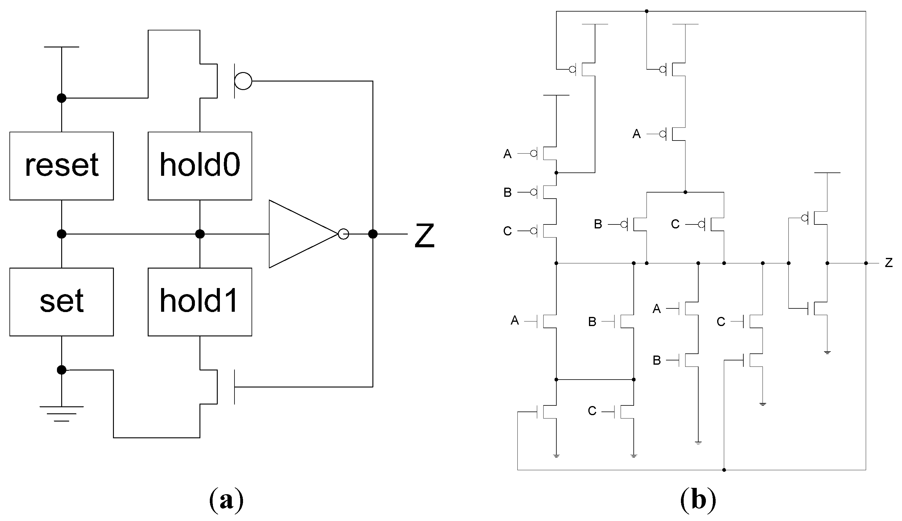
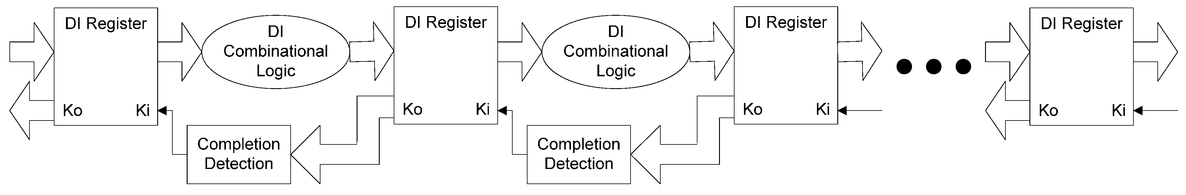
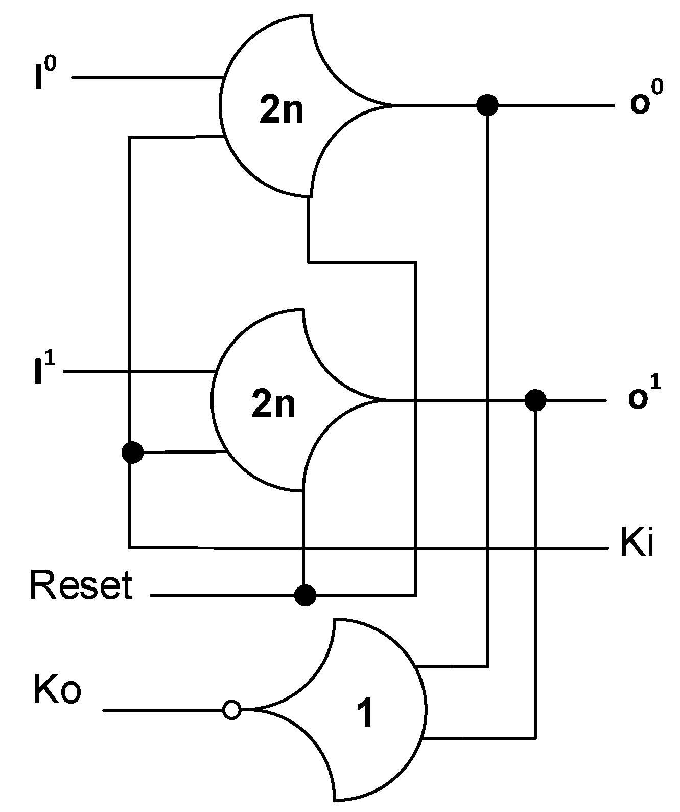
2.1. Introduction to NCL

NCL circuits utilize multi-rail logic, such as dual-rail, to achieve delay-insensitivity. A dual-rail signal, D, consists of two wires, D0 and D1, which may assume any value from the set {DATA0, DATA1, NULL}. The DATA0 state (D0 = 1, D1 = 0) corresponds to a Boolean logic 0, the DATA1 state (D0 = 0, D1 = 1) corresponds to a Boolean logic 1, and the NULL state (D0 = 0, D1 = 0) corresponds to the empty set, meaning that the value of D is not yet available. The two rails are mutually exclusive, such that both rails can never be asserted simultaneously; this state is defined as an illegal state. Dual-rail logic is a space optimal 1-hot delay-insensitive code, requiring two wires per bit.
NCL circuits are comprised of 27 fundamental gates [5]. These 27 gates constitute the set of all functions consisting of four or fewer variables. Here, a variable refers to one rail of a multi-rail signal; hence, a four variable function is not the same as a function of four literals, which would consist of eight variables, assuming dual-rail logic. The primary type of threshold gate, shown in Figure 1, is the THmn gate, where 1 ≤ mn. THmn gates have n inputs; at least m of the n inputs must be asserted before the output will become asserted; and NCL threshold gates are designed with hysteresis state-holding capability, such that all asserted inputs must be de-asserted before the output will be de-asserted. Hysteresis ensures a complete transition of inputs back to NULL before asserting the output associated with the next wavefront of input data. Therefore, a THnn gate is equivalent to an n-input C-element [6] and a TH1n gate is equivalent to an n-input OR gate. Besides the static NCL gate implementation, shown in Figure 2, there are other CMOS implementations, as detailed in [7,8]. In a THmn gate, each of the n inputs is connected to the rounded portion of the gate; the output emanates from the pointed end of the gate; and the gate’s threshold value, m, is written inside of the gate. NCL threshold gates may also include a reset input to initialize the output. These resettable gates are used in the design of Delay-Insensitive (DI) registers [9]; an n inside the gate denotes it as being reset to 0, and a d as reset to 1. A 1-bit NCL register, consisting of two TH22n gates and one inverting TH12 gate, is shown in Figure 3.
NCL systems contain at least two DI registers, one at both the input and at the output, and can be finely pipelined by inserting additional registers, as shown in Figure 4. Two adjacent register stages interact through their request and acknowledge signals, Ki and Ko, respectively, to prevent the current DATA wavefront from overwriting the previous DATA wavefront, by ensuring that the two DATA wavefronts are always separated by a NULL wavefront. The acknowledge signals are combined in the Completion Detection circuitry to produce the request signal(s) to the previous register stage, utilizing either the full-word or bit-wise completion strategy [9].
Figure 1. THmn threshold gate.
Jlpea 05 00216 g001
Figure 2. NCL threshold gate design: (a) General static implementation; (b) TH23 static implementation.
Jlpea 05 00216 g002
Figure 3. 1-Bit NCL register reset to NULL.
Jlpea 05 00216 g003
Figure 4. NCL system framework: input wavefronts are controlled by local handshaking and Completion Detection signals.
Jlpea 05 00216 g004
To ensure delay-insensitivity, NCL circuits must adhere to the following criteria: Input-Completeness and Observability [10]. Input-Completeness requires that all outputs of a combinational circuit may not transition from NULL to DATA until all inputs have transitioned from NULL to DATA, and that all outputs of a combinational circuit may not transition from DATA to NULL until all inputs have transitioned from DATA to NULL. In circuits with multiple outputs, it is acceptable according to Seitz’s “weak conditions” of DI signaling [11] for some of the outputs to transition without having a complete input set present, as long as all outputs cannot transition before all inputs arrive. Observability requires that no orphans may propagate through a gate [12]. An orphan is defined as a wire that transitions during the current DATA wavefront but is not used in the determination of the output. Orphans are caused by wire forks and can be neglected through the isochronic fork assumption [13,14], as long as they are not allowed to cross a gate boundary. This observability condition, also referred to as indicatability or stability, ensures that every gate transition is observable at the output, which means that every gate that transitions is necessary to transition at least one of the outputs.
Reference [15] combines Multi-Threshold CMOS (MTCMOS) with NCL, to yield significant power reduction without any of the drawbacks of applying MTCMOS to synchronous circuits, and is better than the synchronous MTCMOS design in terms of area, energy per operation, and idle power, although the synchronous design can operate faster.

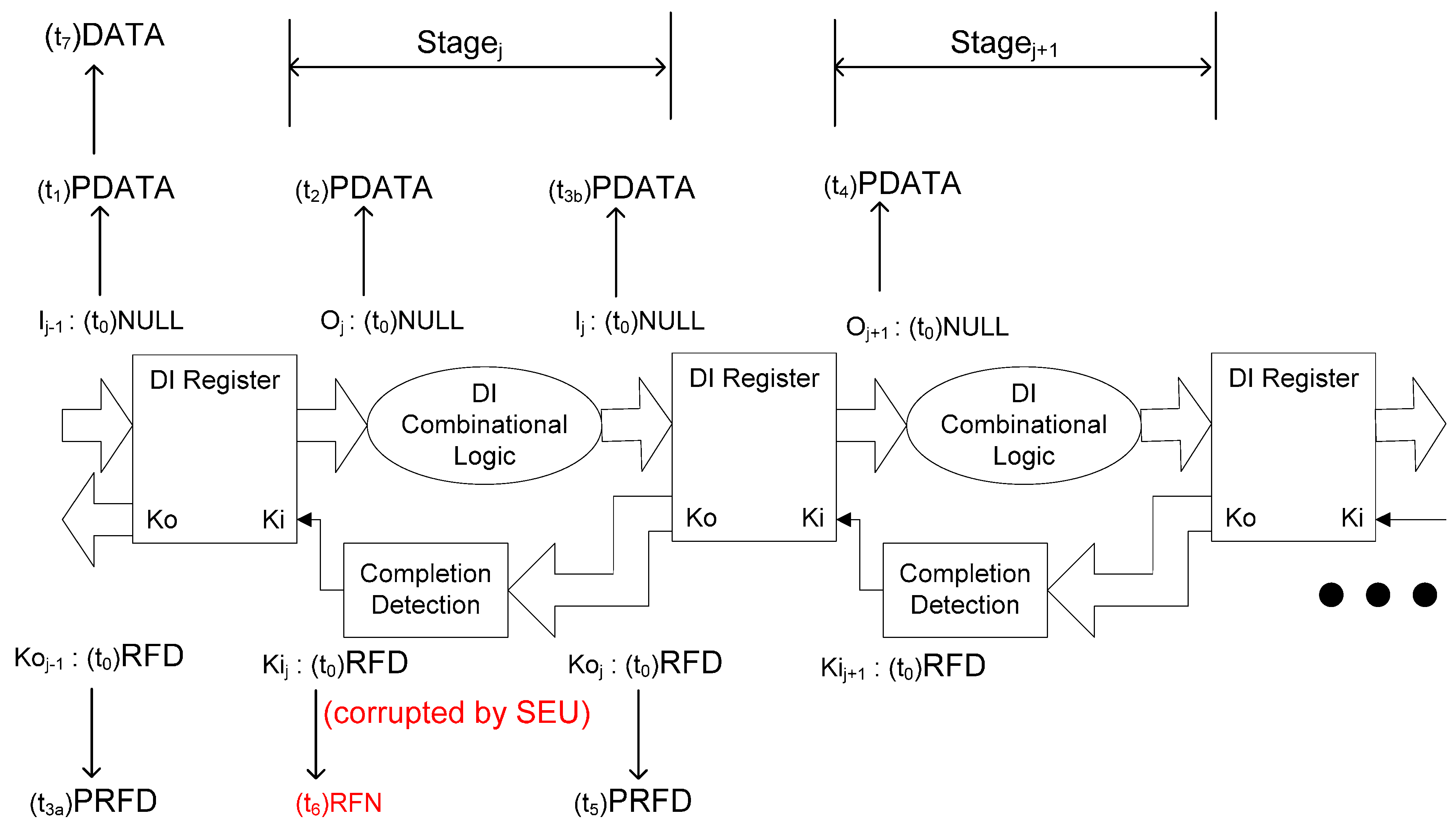
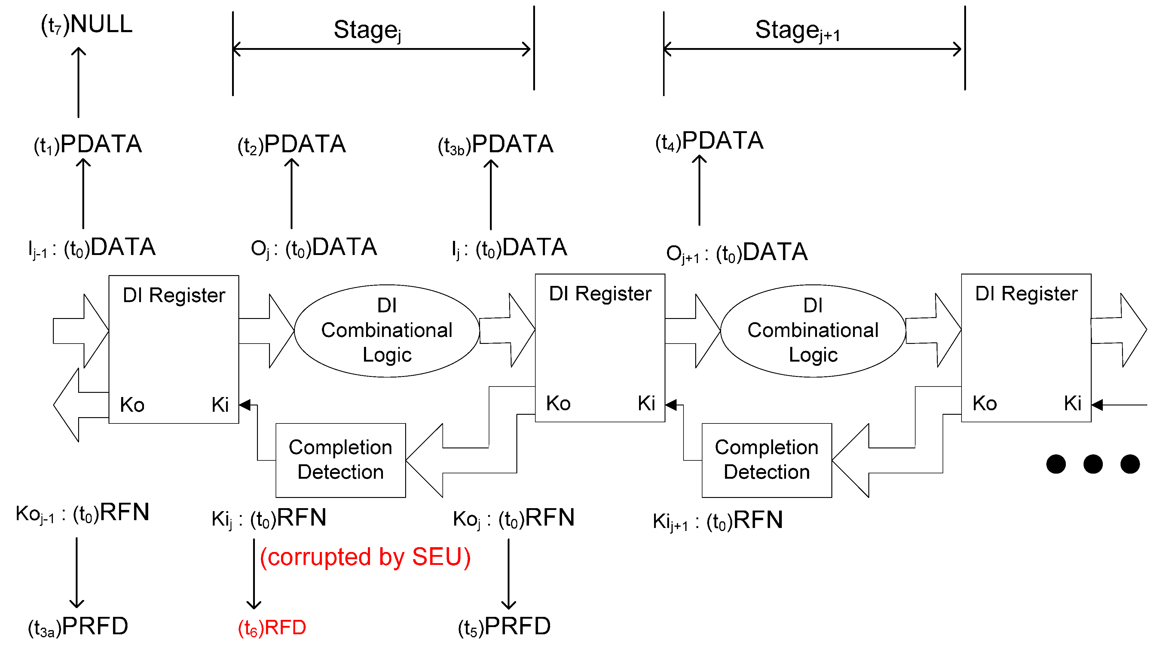
2.2. SEU/SEL Can Cause Deadlock in NCL Systems

It is straightforward to understand that SEU/SEL can cause wrong outputs in NCL systems, and this section shows that SEU/SEL can also cause deadlock, which means that the system is stalled forever and cannot make forward progress. In the following analysis, subscripts are used to specify partial timing order. For example, t1a and t1b both occur earlier than t2, but there is no timing order assumed between t1a and t1b. In addition, a “bit” in this section refers to either a dual-rail data signal or a single-rail acknowledge signal in NCL systems.
In NCL systems, the 1-bit dual-rail data signals composing a multi-bit data signal usually do not change from NULL/DATA to DATA/NULL simultaneously, because of different propagation delays. For example, a 2-bit dual-rail signal can start from {NULL, NULL} at t0, first change to {DATA, NULL} at t1, and eventually change to {DATA, DATA} at t2. Similarly, the 1-bit single-rail acknowledge signals composing a multi-bit acknowledge signal usually do not change from Request-For-DATA (RFD, logic 1)/Request-For-NULL (RFN, logic 0) to RFN/RFD simultaneously, because of different propagation delays. In the following analysis, for a multi-bit data signal, NULL/DATA means that all of the 1-bit dual-rail signals composing it are NULL/DATA, while PDATA means that only part of the 1-bit dual-rail data signals are DATA, while the rest are NULL. Note that NULL, DATA, and PDATA constitute the complete state space of a multi-bit data signal. Similarly, for a multi-bit acknowledge signal, RFN/RFD means that all of the 1-bit single-rail acknowledge signals composing it are RFN/RFD, while PRFD means that only part of the 1-bit single-rail acknowledge signals are RFD, while the rest are RFN. Note that RFN, RFD, and PRFD constitute the complete state space of a multi-bit acknowledge signal.
Figure 5 and Figure 6 illustrate how SEU can cause deadlock during the propagation of a DATA or NULL wavefront, respectively, in which O and I are multi-bit data signals, Ko is a multi-bit acknowledge signal, and Ki is a single-bit acknowledge signal. NCL systems use deadlock-free four-phase handshaking protocol [4], in which a register only allows a DATA/NULL wavefront to pass through after the previous NULL/DATA wavefront has arrived at the output of the subsequent register, which means that deadlock will never occur if Kij of Stagej changes to RFN/RFD only after Oj+1 of Stagej+1 changes to DATA/NULL. Deadlock will occur if Kij is corrupted to RFN/RFD by SEU earlier than expected when Oj+1 is PDATA and Ij-1 is PDATA, which means that only part of the DATA/NULL wavefront has been propagated to Stagej. In that case, Oj will never change to DATA/NULL since Kij has been corrupted to RFN/RFD, which stops the propagation of the DATA/NULL wavefront. Because the DATA/NULL wavefront will never be completely propagated to Stagej after the SEU corruption, deadlock occurs.
As explained in Section 1, the SEL fault model assumes that the states of multiple gates may be corrupted, while the SEU fault model only assumes state corruption of a single gate. As a result, it is straightforward to understand that SEL can also cause deadlock in NCL systems.
Figure 5. SEU can cause deadlock during the propagation of a DATA wavefront.
Jlpea 05 00216 g005
Figure 6. SEU can cause deadlock during the propagation of a NULL wavefront.
Jlpea 05 00216 g006

2.3. Radiation Hardened Digital Circuit Design

An SEU resistant design methodology [16,17,18,19] was proposed for asynchronous circuits implemented with Pre-Charged Half Buffers (PCHB). This methodology can make a PCHB circuit immune to SEU all the time. The idea is to double the circuit and use TH22 gates to stop the propagation of corrupted data and acknowledge/request signals. Although the TH22 gates can stop the propagation of corrupted signals internally, the correct output cannot be inferred from the outputs of just one copy, as the outputs of that copy may be corrupted by SEU. As long as the outputs of both of the two copies are observable, the methodology makes the circuit completely SEU resistant. Other methodologies [20,21,22] have been proposed to design NCL circuits with reduced possibility that SEU may cause deadlock or wrong data, but none of them can make NCL circuits completely SEU resilient.
References [23,24] propose an SEL resistant design methodology for memories. The circuit is first duplicated and then divided into several redundant groups in such a way that if the states of one group are corrupted by SEL, they can be recovered from the states of other groups by error correcting codes. A power management unit connects the global power supply line to many virtual power supply lines by current-limiting transistors. Each virtual power supply line is used by only one group, and each group has a current comparator monitoring its virtual supply current. When SEL occurs, it will not cause permanent damage, as the surge current of one group will be detected by its current comparator and limited by turning off its current-limiting transistor. Once the SEL effect disappears and the current comparator of the affected group detects that the current has decreased to a normal value, the current-limiting transistor is turned back on to resume the virtual power supply of the affected group. The data of that group are lost, but can be recovered from the states of other groups, such that no data is lost in the system. However, no schemes have previously been proposed to make QDI circuits, including NCL circuits, completely SEL resilient.

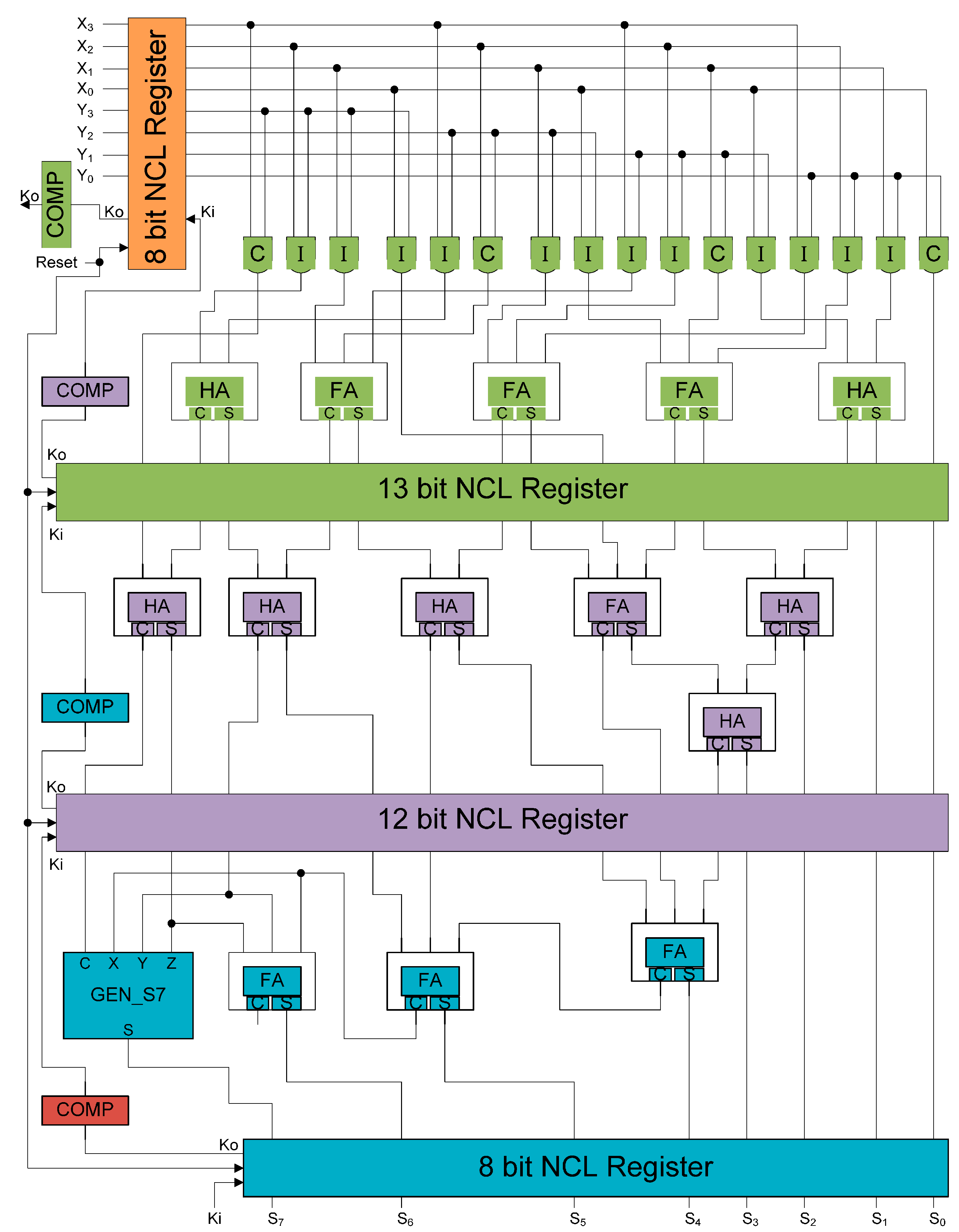
3. Design Methodology

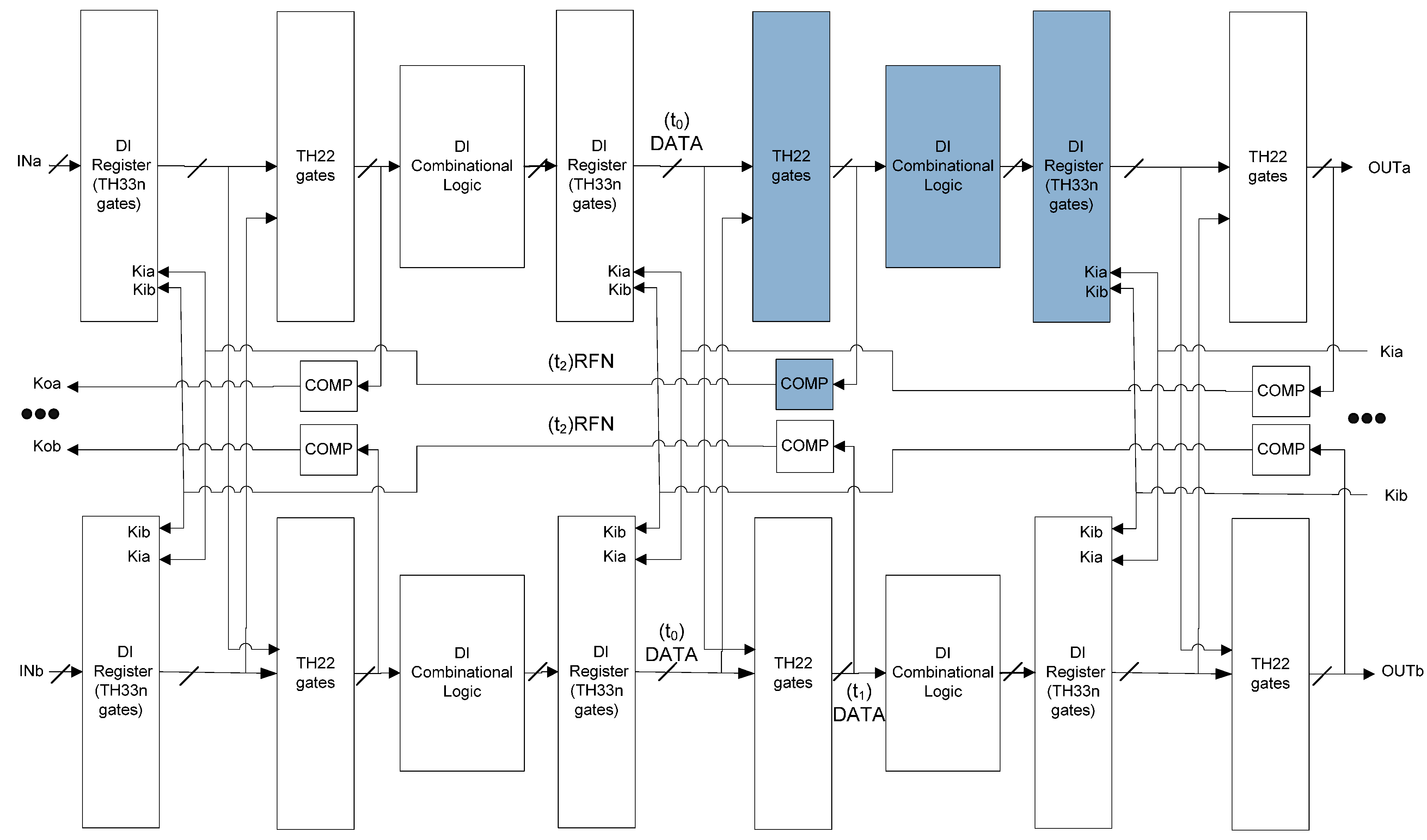
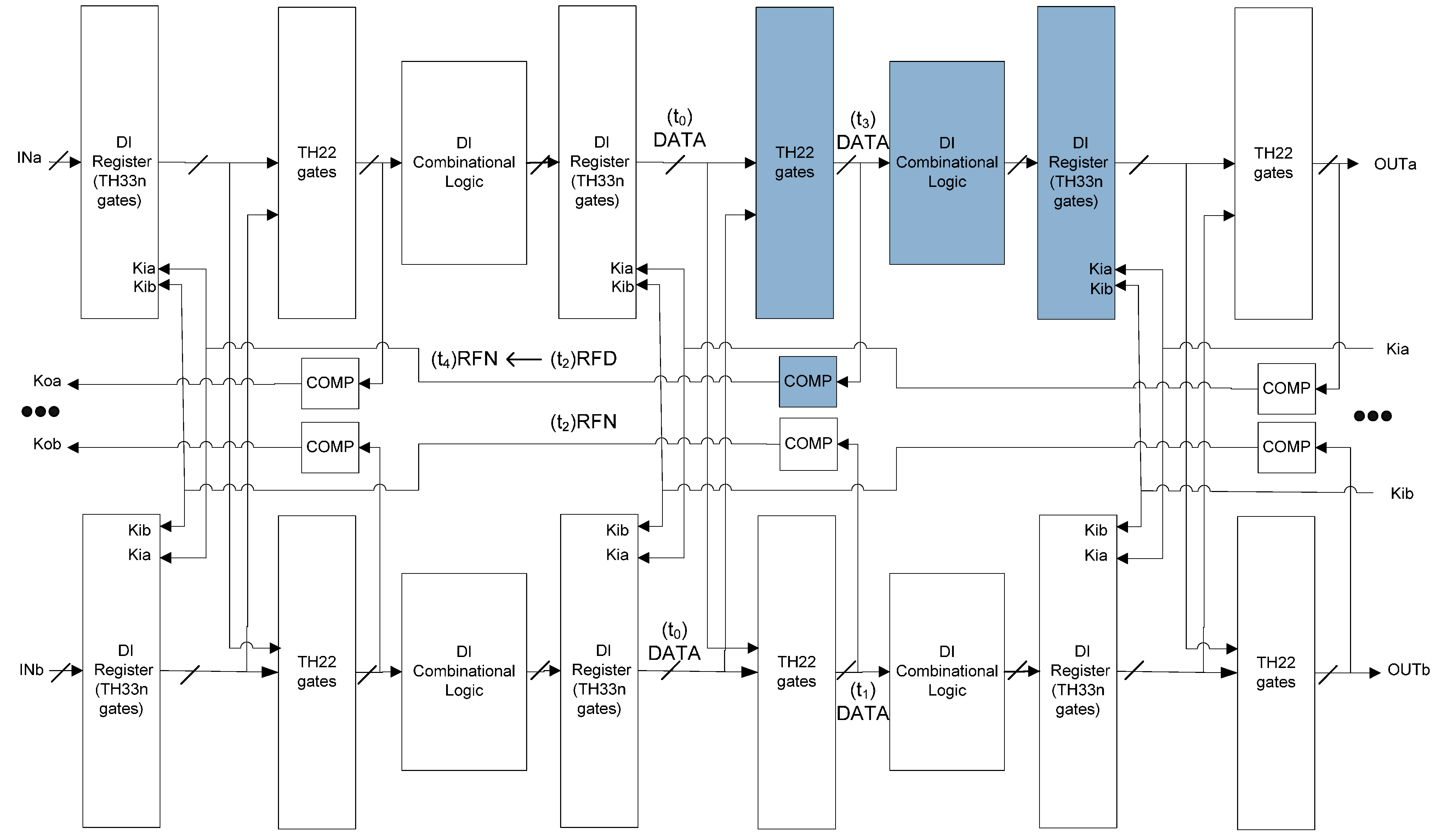
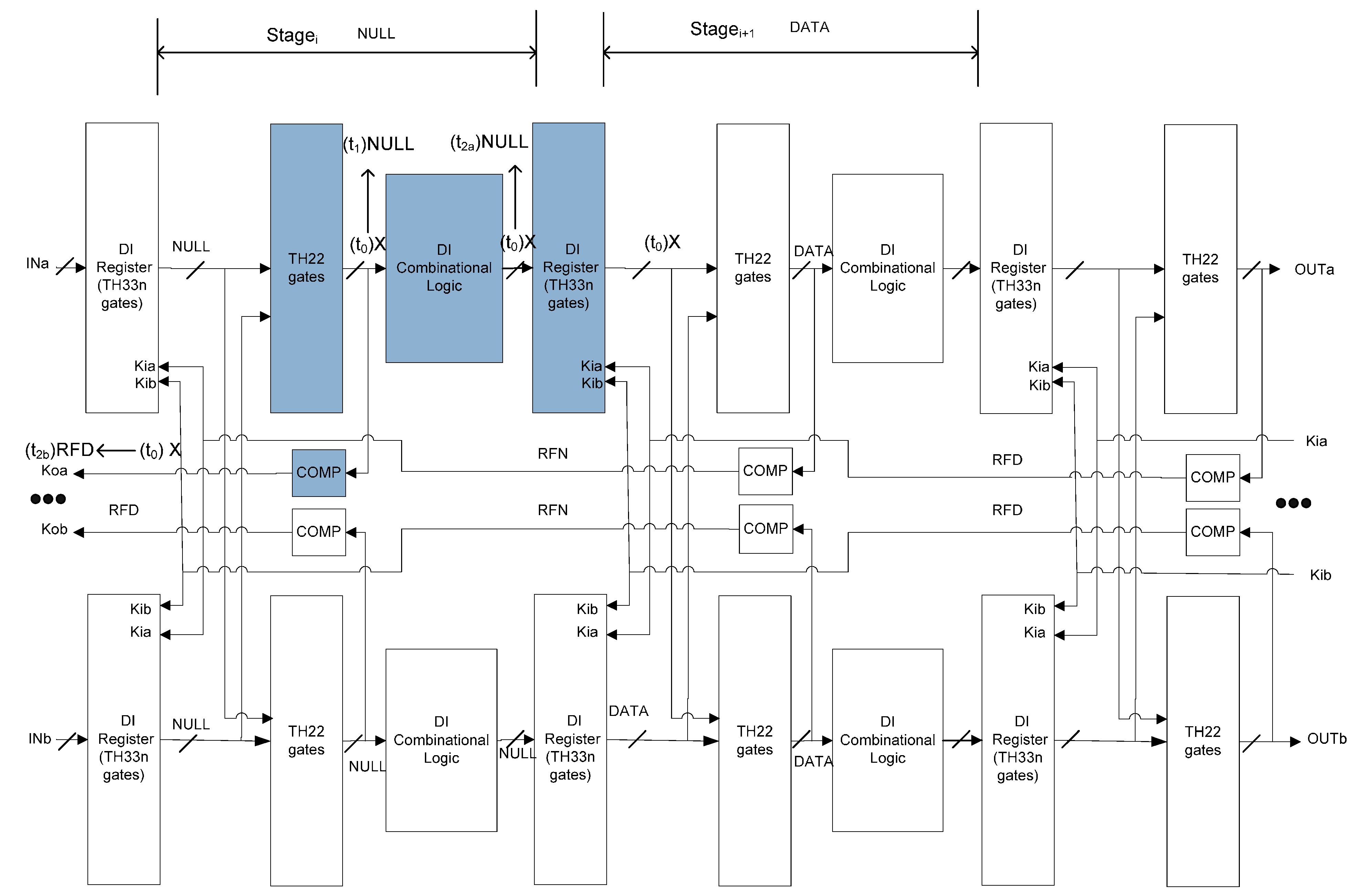
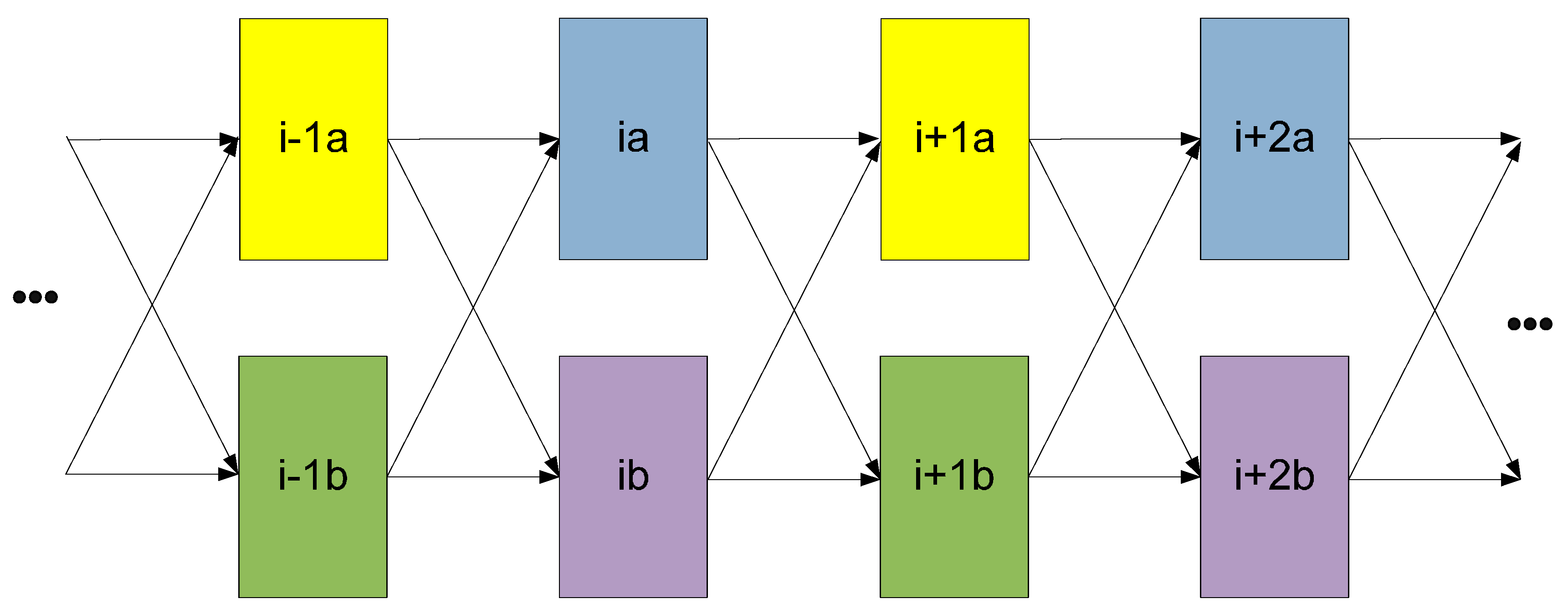
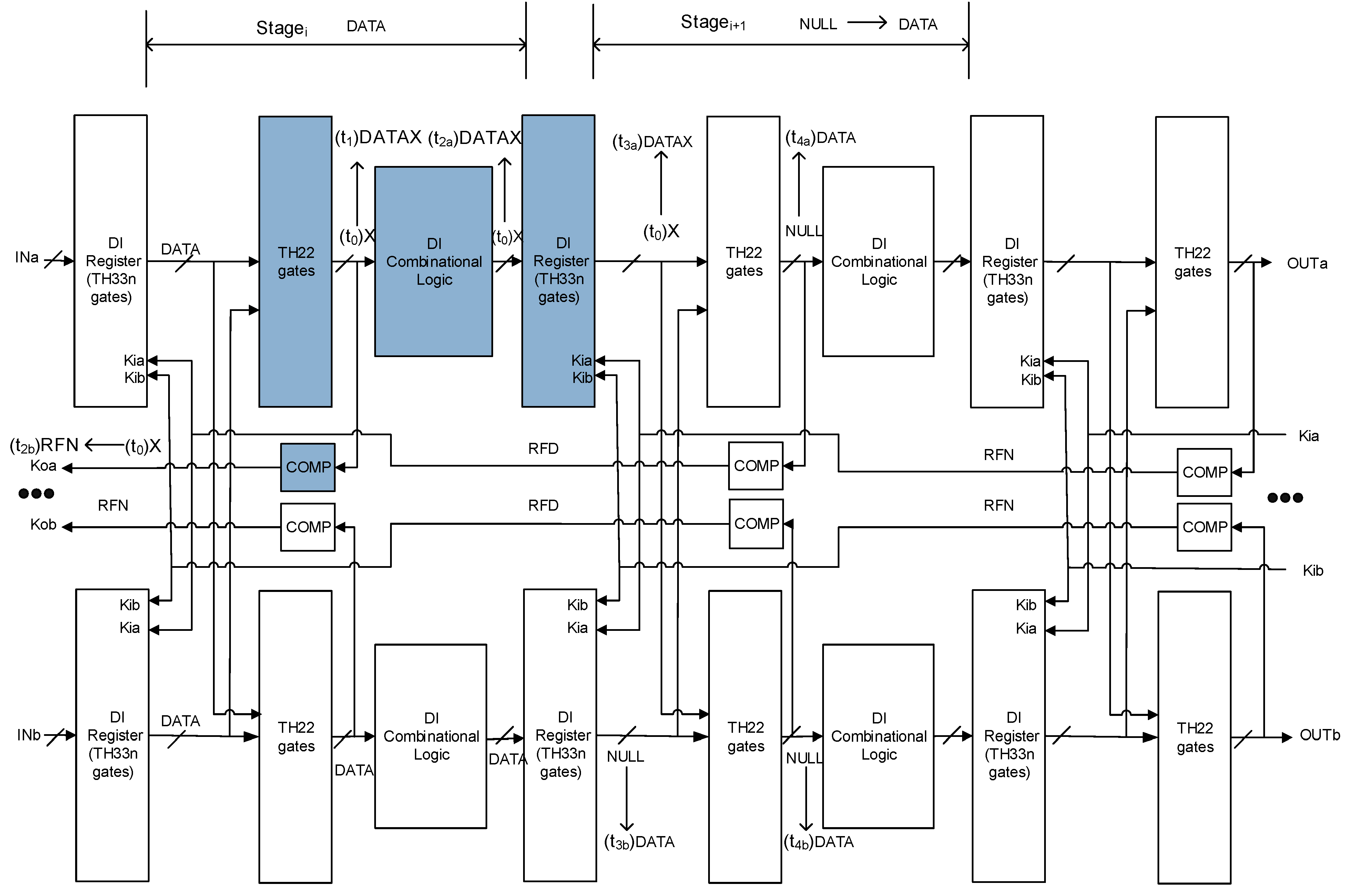
3.1. SEL/SEU Resistant NCL Architecture

This paper proposes an SEL/SEU resistant NCL architecture, shown in Figure 7. Starting from the original NCL architecture in Figure 4, the following four steps are required to make it SEU resistant:
  • Double the original circuit.
  • Replace TH22n gates in the original NCL register with TH33n gates that accept acknowledge signals from both copies.
  • Insert TH22 gates at the output of NCL registers that accept register outputs from both copies.
  • Move the inverting TH12 gate in the original NCL register and Completion Detection from the outputs of NCL registers to the outputs of the added TH22 gates. The resulting Completion Logic, COMP, in Figure 7 consists of the original Completion Detection in Figure 4 and the inverting TH12 gates moved from the original NCL register.
Note that the power management unit with current-limiting transistors and current comparators is not required to make a design SEU resistant, since SEU can only change the output of a single gate and can never cause permanent damage by huge current as can SEL. The proposed SEU resistant NCL architecture will stop the propagation of a corrupted state, so as to not cause deadlock or a wrong output, which is proved in Section 4.
As mentioned in Section 2.3, a circuit is SEL resistant if it can be divided into several groups with separate virtual power supplies, and has the property that if the power supply of one group is cut off and resumed later, the information stored in that group can be recovered from other intact groups without causing a wrong output or deadlock. The fewer groups the circuit is divided into, the smaller the area overhead, since less current-limiting transistors and current comparators will be required.
The inserted TH22 gates, the following Completion Logic, Combinational Circuit, and NCL register can be put into one group, as shaded in Figure 7. Section 4 proves that this division scheme is SEL resistant, and by extension proves that it is SEU resistant as well, because the SEL fault model assumes that the states of an entire group may be corrupted, while the SEU fault model only assumes state corruption of a single gate. This division scheme is optimized in Section 5 by combining the initial groups systematically to yield an optimal 4-group division.
The analog circuit design of the current comparator and current-limiting transistors is beyond the scope of this paper. For example, the power management unit designed in [23,24] can be utilized with the proposed SEL/SEU resistant architecture.
Figure 7. SEL/SEU resistant NCL architecture.
Jlpea 05 00216 g007

3.2. Area and Speed Overhead

Compared with the original NCL architecture, the SEL/SEU resistant NCL architecture doubles the area of the Combinational Logic and Completion Detection. The Register area of the SEL/SEU resistant architecture is almost four times as large as that of the original architecture, since two TH22n gates and one inverting TH12 gate in the original 1-bit NCL register are replaced with four TH33n gates, four inserted TH22 gates and two inverting TH12 gates. Therefore, the logic area overhead is approximately bounded between 2× and 4× the original, depending on how finely the original NCL circuit is pipelined. The more finely the original NCL circuit is pipelined, the larger the area overhead. There will be no extra area overhead if the resulting architecture is only required to be SEU resistant. If it is required to be SEL resistant as well, a power management unit will be needed, which will increase overhead.
In NCL circuits, the DATA-to-DATA cycle time (TDD) [9] has an analogous role to the clock period in a synchronous system and is the reciprocal of throughput. If a gate delay is used as the minimal delay unit, and stagei has TCOMBi and TCOMPi gate delays in the Combinational Logic and Completion Detection, respectively, the original NCL circuit’s TDD = max (2 × (2.5 + TCOMBi + TCOMPi)) for i in all of the stages [25]. The formula was derived from the fact that stagei propagates a DATA/NULL wavefront and generates the acknowledge signal to the previous stage during half of the TDD, with one gate delay through the input register, TCOMBi gate delays through the Combinational Logic, one gate delay through the output register, 0.5 gate delay though the inverting TH12 gate inside the output register, and TCOMPi gate delays through the Completion Detection.
Using the same method, it can be derived that stagei in the proposed SEL/SEU resistant NCL architecture propagates a DATA/NULL wavefront and generates the acknowledge signal to the previous stage during half of its TDD, with one gate delay through the input register, one gate delay through stagei’s inserted TH22 gates, TCOMBi gate delays through the Combinational Logic, one gate delay through the output register, one gate delay through stagei+1’s inserted TH22 gates, 0.5 gate delay though the inverting TH12 gate inside COMP, and TCOMPi gate delays through the Completion Detection inside COMP. Therefore, the SEL/SEU resistant NCL circuit’s TDD = max (2 × (4.5 + TCOMBi + TCOMPi)) for i in all of the stages. The more finely the original NCL circuit is pipelined, the larger the speed overhead, since four gate delays are added to the critical path, regardless of stage size.

4. SEL/SEU Resistance Proof

This section proves that the proposed architecture can recover from SEL effects without causing deadlock or incorrect output. As mentioned in Section 2.3, when SEL occurs, it will be detected by the current comparator of the affected group, which causes the power management unit to cut off the virtual power supply of that group by turning off its current-limiting transistor. Once the SEL effect disappears and the current comparator of the affected group detects that the current has decreased to a normal value, the current-limiting transistor is turned back on to resume the virtual power supply of the affected group. Then the states of all gates in that group become unknown, which can be either logic 1, logic 0, or even at a voltage level between logic 1 and logic 0 transiently, and will be re-evaluated according to the outputs of other intact groups once the power supply is reconnected. In the following analysis, the unknown state is referred to as X. DATAX refers to a corrupted DATA state, in which a rail that should be 0 has changed to X. For example, if the correct DATA state of a dual-rail signal is (D0 = 0, D1 = 1), then the DATAX state of that signal is (D0 = X, D1 = 1). Subscripts are used to specify partial timing order in the following analysis. For example, t1a and t1b are both earlier than t2, but there is no timing order specified between t1a and t1b. Note that DI Combinational Logic is monotonic [20], which means if the Combinational Logic's input changes to DATAX/NULL, its output will eventually change to DATAX/NULL, even if all of the internal states of the Combinational Logic are unknown before the change.

4.1. SEL Will Not Cause Deadlock

In the four-phase handshaking protocol used by NCL, a register only allows a DATA/NULL wavefront to pass through after the previous NULL/DATA wavefront has arrived at the output of the subsequent register. As explained in Section 2.2, deadlock will occur if and only if this protocol is violated.
If both Kia and Kib of an NCL register become Request-For-NULL (RFN, logic 0), that register will allow a NULL wavefront to pass through, so it needs to be proved that the previous DATA wavefront has arrived at the output of the subsequent register. As shown in Figure 8, at t2 both Kia and Kib became RFN. At least one of Kia and Kib was not corrupted by SEL because the two signals are in different groups. Assuming Kib was not affected by SEL, it can be deduced that at t1 the outputs of copyb’s inserted TH22 gates became DATA, and can be further deduced that at t0 the outputs of the two copies of the previous register both became DATA, which corresponds to the handshaking protocol. A corner case exists when at t2 Kia was corrupted to RFD instead. As shown in Figure 9, at t3 the output of the inserted TH22 gates will change to DATA, since both inputs of the inserted TH22 gates are DATA. The inserted TH22 gates drive the Completion Logic and will eventually correct Kia to RFN at t4 so that the system can make forward progress. Similarly, it can be proved that deadlock will not happen during the propagation of the DATA wavefront by exchanging NULL with DATA and RFN with Request-For-DATA (RFD, logic 1) in the above analysis.
Figure 8. SEL will not cause deadlock.
Jlpea 05 00216 g008
Figure 9. SEL will not cause deadlock in the corner case.
Jlpea 05 00216 g009

4.2. SEL Will Not Cause Incorrect Output

In NCL circuits, each valid data token can occupy one or more consecutive register stages storing DATA and two valid data tokens are always separated by one or more consecutive register stages storing NULL. Therefore, the worst case to prove that SEL will not cause wrong output is when the NCL circuit contains the largest number of data tokens, which means the outputs of consecutive register stages alternate between DATA and NULL. The following two scenarios are discussed respectively: when the register in the group affected by SEL stored NULL and when it stored DATA.
Figure 10 shows the scenario when the register in the group affected by SEL stored NULL. The virtual power supply of that group was resumed at t0 so that the states of all gates in that group became X. The X states cannot pass through the inserted TH22 gates, since the output of the register of the other copy is intact NULL. At t1, the output of the TH22 gates in the affected group change to DATAX, because the inputs of the TH22 gates are intact DATA from both copies. At t2a, the output of the Combinational Logic in the affected group changes to DATAX, because of the monotonic property of DI Combinational Logic. At t2b, the output of the Completion Logic in the affected group changes to RFN, which corresponds to the handshaking protocol. It can be expected that when DATAX in stagei propagates to stagei+1 at t3a, it will be filtered to be correct DATA at t4a by the inserted TH22 gates and the intact DATA from the other copy. The DATAX states left in the affected group will eventually be flushed by intact NULL states from both copies, once the NULL wavefront starts propagating from stagei-1 to stagei. Therefore, when the register in the group affected by SEL stored NULL, no incorrect output will be produced.
Figure 10. SEL will not cause incorrect output (the first of the two possible scenarios).
Jlpea 05 00216 g010
Figure 11 shows the scenario when the register in the group affected by SEL stored DATA. The power supply of that group was resumed at t0 so that the states of all gates in that group became X. The X states cannot pass through the inserted TH22 gates, since the output of the register of the other copy is intact DATA. At t1, the output of the TH22 gates in the affected group changed to NULL, because the inputs of the TH22 gates are intact NULL from both copies. At t2a, the output of the Combinational Logic in the affected group changed to NULL, because of the monotonic property of DI Combinational Logic. At t2b, the output of the Completion Logic in the affected group changed to RFD, which corresponds to the handshaking protocol. The X states left in the affected group will eventually be flushed by the NULL states at the output of the Combinational Logic of the same group, once the NULL wavefront starts propagating from stagei to stagei+1. Therefore, when the register in the group affected by SEL stored DATA, no wrong output will be produced.
Since it has been proved that even if the outputs of all gates in a group are corrupted, SEL will not cause deadlock or wrong output in the worst case, the proposed architecture is SEL resistant. As a result, the proposed architecture is SEU resistant by extension, because the SEL fault model assumes the states of an entire group may be corrupted, while the SEU fault model only assumes state corruption of a single gate.
Figure 11. SEL will not cause incorrect output (the second of the two possible scenarios).
Jlpea 05 00216 g011

5. Optimal Four-Group Division

The data flow graph of the group division scheme proposed in Section 3 is shown in Figure 12, in which forward arrows represent data signals, excluding Ki and Ko signals generated by Completion Logic. It can be observed from the proof in Section 4 that the recovery from SEL of one group (e.g., groupia) only depends on the intact states of the previous stage (groupi-1a and groupi-1b), the next stage (groupi+1a and groupi+1b), and the other copy of the same stage (groupib). Therefore, all groups of every other stage in one copy (e.g., ..., groupi-2a, groupia, groupi+2a, ...) can be combined into one group to yield the optimal four-group division, annotated by four colors in Figure 12.
Figure 12. Data flow graph and the optimal 4-group division.
Jlpea 05 00216 g012

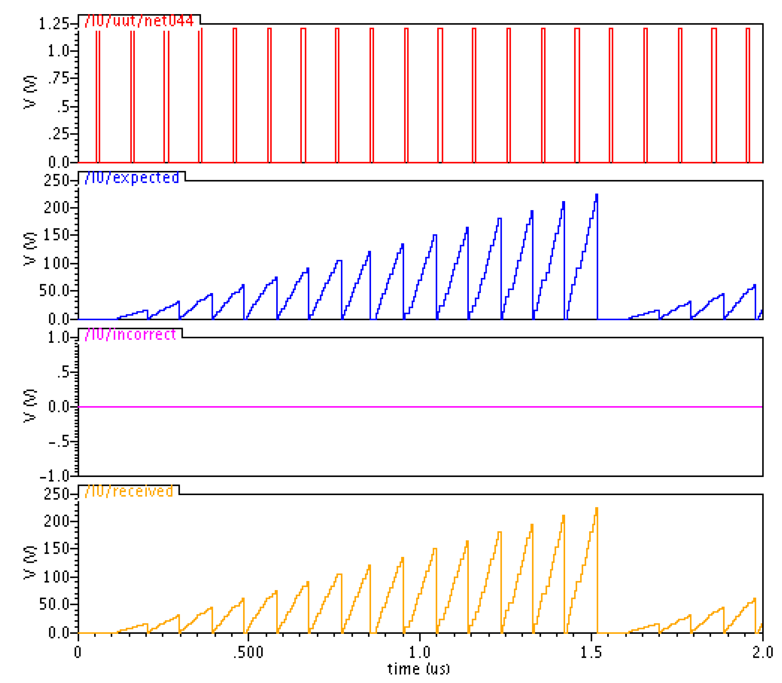
6. Simulation Results

A three-stage full-word pipelined NCL 4 × 4 unsigned multiplier [9] was transformed to its SEL/SEU resistant version using the four-group optimal division scheme. Annotated by different colors in Figure 13, the initial grouping yields five groups per copy, which is 10 groups in total before being combined into four groups with the optimized scheme described in Section 5. The design was implemented at the transistor level using the IBM cmrf8sf 130 nm 1.2 V process, and simulated with the Cadence Ultrasim simulator. A VerilogA controller was designed to input data and check the output automatically. The interface protocol is as follows: in the SEL/SEU resistant NCL architecture presented in Figure 7, when Koa and Kob are both RFD/RFN, input DATA/NULL to both INa and INb; when both OUTa and OUTb are NULL, change both Kia and Kib to RFD; when both OUTa and OUTb are DATA or one is DATA and the other is DATAX, change both Kia and Kib to RFN, as correct DATA can be inferred from DATA and DATAX.
Figure 13. Initial grouping per copy of a three-stage NCL 4 × 4 multiplier.
Jlpea 05 00216 g013
The VerilogA controller also acts as the power management unit in the simulation by cutting off the power supply of the affected group according to an active high SEL fault injection signal with 100 ns period and 10% duty cycle, independent of input/output handshaking. In real hardware, the power management unit turns off the current-limiting transistor of one group usually for several microseconds to ensure the SEL disappears; in simulation, the pulse was made much longer to cover the worst case. In real hardware, when the current-limiting transistor of one group is turned off, there will be huge voltage drop at the virtual power supply line of that group; in simulation, the VerilogA controller forces the virtual power supply to ground to cover the worst case. If the SEL fault injection signal is kept high, the pipeline will be stalled eventually. Once the SEL fault injection signal falls, the VerilogA controller forces the virtual power supply to the global power supply value and the pipeline starts recovering with the mechanism described in Section 4.
In each simulation, one of the four groups was injected with an SEL fault, and the 4 × 4 unsigned multiplier was exhaustively tested with all input combinations by incrementing input Y every data token and input X every 16 data tokens. The VerilogA controller automatically calculates the expected output data from the input sequence, infers the received output data from the monitored OUTa and OUTb, and asserts an active high error signal if the received out data does not match the expected output. The VerilogA controller outputs these validation signals as voltages in a dumped waveform. In total, four simulations were run to cover SEL occurrences in all of the four groups; and SEL did not cause deadlock or wrong output in any of them. The waveform of one such simulation is shown in Figure 14, in which the signals are as follows, from top to bottom: the active high SEL fault injection signal, the expected output, the active high error signal, and the received output. Since the Cadence Ultrasim simulator can only dump signals in voltage or current format, the expected and received output were dumped as voltage signals in the waveform. For example, 225 volt means the expected/received output was 225 (15 × 15).
Figure 14. Simulation with SEL fault injection.
Jlpea 05 00216 g014
Without fault injection and with the same input pattern, the original NCL multiplier and the SEL/SEU resistant NCL multiplier, without a hardware power management unit, were also simulated for speed (average TDD), area, and energy per operation. The results are shown in Table 1. Compared to the original version, the SEU/SEL hardened architecture has 1.31× speed overhead, 2.74× area overhead, and 2.79× energy per operation overhead.
Table 1. Simulation results.
Circuit TypeTransistor#TDD (ns)Energy/Operation (pJ)
Original NCL16957.21.05
SEL/SEU resistant NCL46469.42.93

7. Conclusions

This paper proposes a radiation hardened NCL architecture that can recover from an SEL or SEU fault without deadlock or any data loss. The proposed architecture is analytically proved to be SEL resistant, which by extension proves it to also be SEU resistant. The SEL/SEU resistant version of a three-stage full-word pipelined NCL 4 × 4 unsigned multiplier was implemented using the IBM cmrf8sf 130 nm 1.2 V process at the transistor level and simulated exhaustively with SEL fault injection to validate the proposed architecture. Compared with the original version, the SEL/SEU resistant version has 1.31× speed overhead, 2.74× area overhead, and 2.79× energy per operation overhead.

Author Contributions

All authors conceived and designed the proposed architecture; Liang Zhou performed the simulations; and all authors analyzed the results and wrote the paper.

Conflicts of Interest

The authors declare no conflict of interest.

References

  1. Dodd, P.E.; Massengill, L.W. Basic Mechanisms and Modeling of Single-Event Upset in Digital Microelectronics. IEEE Trans. Nucl. Sci. 2003, 50, 583–602. [Google Scholar]
  2. Shoga, M.; Binder, D. Theory of single event latchup in complementary metal-oxide semiconductor integrated circuits. IEEE Trans. Nucl. Sci. 1986, 33, 1714–1717. [Google Scholar]
  3. Martin, A.J. The Limitations to Delay-Insensitivity in Asynchronous Circuits; Springer: New York, NY, USA, 1990; pp. 302–311. [Google Scholar]
  4. Fant, K.M.; Brandt, S.A. NULL Convention Logic: A Complete and Consistent Logic for Asynchronous Digital Circuit Synthesis. In Proceedings of the International Conference on Application Specific Systems, Architectures and Processors, Chicago, IL, USA, 19–21 August 1996; pp. 261–273.
  5. Sobelman, G.E.; Fant, K.M. CMOS Circuit Design of Threshold Gates with Hysteresis. In Proceedings of the 1998 IEEE International Symposium on Circuits and Systems (II), Monterey, CA, USA, 31 May–3 June 1998; pp. 61–65.
  6. Muller, D.E. Asynchronous Logics and Application to Information Processing. In Switching Theory in Space Technology; Stanford University Press: Redwood City, CA, USA, 1963; pp. 289–297. [Google Scholar]
  7. Parsan, F.A.; Smith, S.C. CMOS Implementation of Static Threshold Gates with Hysteresis: A New Approach. In Proceedings of the IFIP/IEEE International Conference on VLSI-SoC, Santa Cruz, CA, USA, 7–10 October 2012; pp. 41–45.
  8. Parsan, F.A.; Smith, S.C. CMOS Implementation Comparison of NCL Gates. In Proceedings of the IEEE International Midwest Symposium on Circuits and Systems, Boise, ID, USA, 5–8 August 2012; pp. 394–397.
  9. Smith, S.C.; DeMara, R.F.; Yuan, J.S.; Hagedorn, M.; Ferguson, D. Delay-Insensitive Gate-Level Pipelining. Elsevier’s Integr. VLSI J. 2001, 30, 103–131. [Google Scholar] [CrossRef]
  10. Smith, S.C.; DeMara, R.F.; Yuan, J.S.; Ferguson, D.; Lamb, D. Optimization of NULL convention self-timed circuits. Integr. VLSI J. 2004, 37, 135–165. [Google Scholar] [CrossRef]
  11. Seitz, C.L. System Timing. In Introduction to VLSI Systems; Addison-Wesley: Boston, MA, USA, 1980; pp. 218–262. [Google Scholar]
  12. Kondratyev, A.; Neukom, L.; Roig, O.; Taubin, A.; Fant, K. Checking Delay-Insensitivity: 104 Gates and Beyond. In Proceedings of the Eighth International Symposium on Asynchronous Circuits and Systems, Manchester, UK, 8–11 April 2002; pp. 149–157.
  13. Martin, A.J. Programming in VLSI: From Communicating Processes to Delay-Insensitive Circuits. In Developments in Concurrency and Communication; UT Year of Programming Institute on Concurrent Programming, Addison-Wesley: Boston, MA, USA, 1990; pp. 1–64. [Google Scholar]
  14. Van Berkel, K. Beware the isochronic fork. Integr. VLSI J. 1992, 13, 103–128. [Google Scholar] [CrossRef]
  15. Zhou, L.; Parameswaran, R.; Parsan, F.A.; Smith, S.C.; Di, J. Multi-Threshold NULL Convention Logic (MTNCL): An ultra-low power asynchronous circuit design methodology. J. Low Power Electron. Appl. 2015, 5, 81–100. [Google Scholar] [CrossRef]
  16. Jiang, W.; Martin, A.J. A Soft-Error Tolerant Asynchronous Microcontroller. In Proceedings of the 13th NASA Symposium on VLSI Design, Post Falls, ID, USA, 4–5 June 2007.
  17. Jiang, W.; Martin, A.J. Soft-Error Robustness in QDI Circuits. In Proceedings of the 1st Workshop on System Effects of Logical Soft Errors, Urbana-Champaign, IL, USA, 5–6 April 2005.
  18. Jiang, W.; Martin, A.J. SEU-Tolerant QDI Circuits. In Proceedings of the 11th IEEE International Symposium on Asynchronous Systems & Circuits, New York, NY, USA, 14–16 March 2005; pp. 156–165.
  19. Jiang, W.; Martin, A.J. Soft-Error Tolerant Asynchronous FPGA. In Proceedings of the Dependable System and Network 2005, Rio de Janeiro, Brazil, 22–25 June 2005.
  20. Kuang, W.; Zhao, P.; Yuan, J.S.; DeMara, R.F. Design of asynchronous circuits for high soft error tolerance in deep submicron CMOS Circuits. IEEE Trans. VLSI Syst. 2010, 18, 410–422. [Google Scholar] [CrossRef]
  21. Kuang, W.; Ibarra, C.M.; Zhao, P. Soft Error Hardening for Asynchronous Circuits. In Proceedings of the 22nd IEEE International Symposium on Defect and Fault-Tolerance in VLSI Systems, Rome, Italy, 26–28 September 2007; pp. 273–281.
  22. Kuang, W.; Xiao, E.; Ibarra, C.M.; Zhao, P. Design Asynchronous Circuits for Soft Error Tolerance. In Proceedings of the IEEE International Conference on Integrated Circuit Design and Technology, Austin, TX, USA, 30 May–1 June 2007; pp. 1–5.
  23. Nicolaidis, M. A Low-Cost Single-Event Latchup Mitigation Scheme. In Proceedings of the 12th IEEE International Symposium on On-Line Testing, Lake Como, Italy, 10–12 July 2006; pp. 111–118.
  24. Nicolaidis, M.; Torki, K.; Natali, F.; Belhaddad, F.; Alexandrescu, D. Implementation and Validation of a Low-Cost Single-Event Latchup Mitigation Scheme. In Proceedings of the IEEE Workshop on Silicon Errors in Logic-System Effects, Stanford, CA, USA, 24 March 2009.
  25. Zhou, L.; Smith, S.C. Accurate Throughput Derivation of Pipelined NULL Convention Logic Asynchronous Circuits. In Proceedings of the International Conference on Computer Design, Las Vegas, NV, USA, 16–19 July 2012; pp. 51–54.

