1. Dendrites for Wordspotting
Dendrites are highly branched tree like structures that connect neuron’s synapses to the soma. They were previously believed to act just like wires and have little or no computational value. However, studies show that dendrites are computational subunits that perform some inherent processing that contributes to overall neural computation [
1,
2,
3,
4,
5,
6]. It is thus interesting to explore computational models that can be built using dendrites as a unit. It has been shown that dendrites can perform computations similar to an HMM branch [
3,
7] which can be used for wordspotting. Wordspotting is the detection of small set of words in unconstrained speech [
8]. The interlink between Neuroscience, CMOS transistors and HMMs is shown in
Figure 1a.
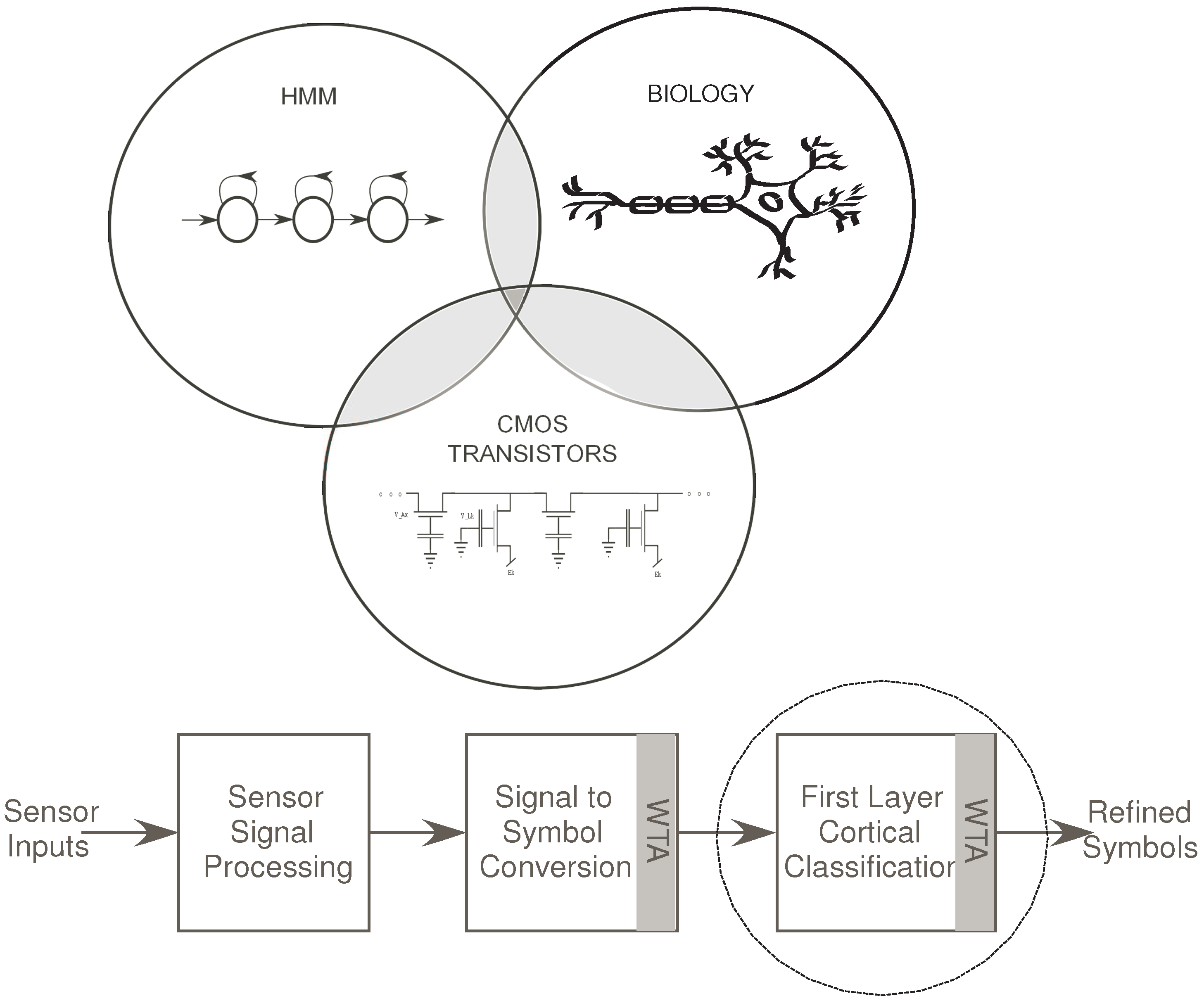
Figure 1.
(a) The Venn Diagram depicts the interlinks between the fields of neurobiology, HMM structures and CMOS transistors. We have demonstrated in the past how we can build reconfigurable dendrites using programmable analog techniques. We have also shown how such a dendritic network can be used to build an HMM classifier which is typically used for speech recognition systems; (b) Block Diagram for a Speech/Pattern Recognition system with respect to biology. In a typical speech recognition system, we have an auditory front-end processing block, a signal to symbol conversion block and a state decoding block for classification. We have implemented the state decoding block using dendritic branches, WTA and supporting circuitry for wordspotting. It is the classification stage before which symbols have been generated for a word.
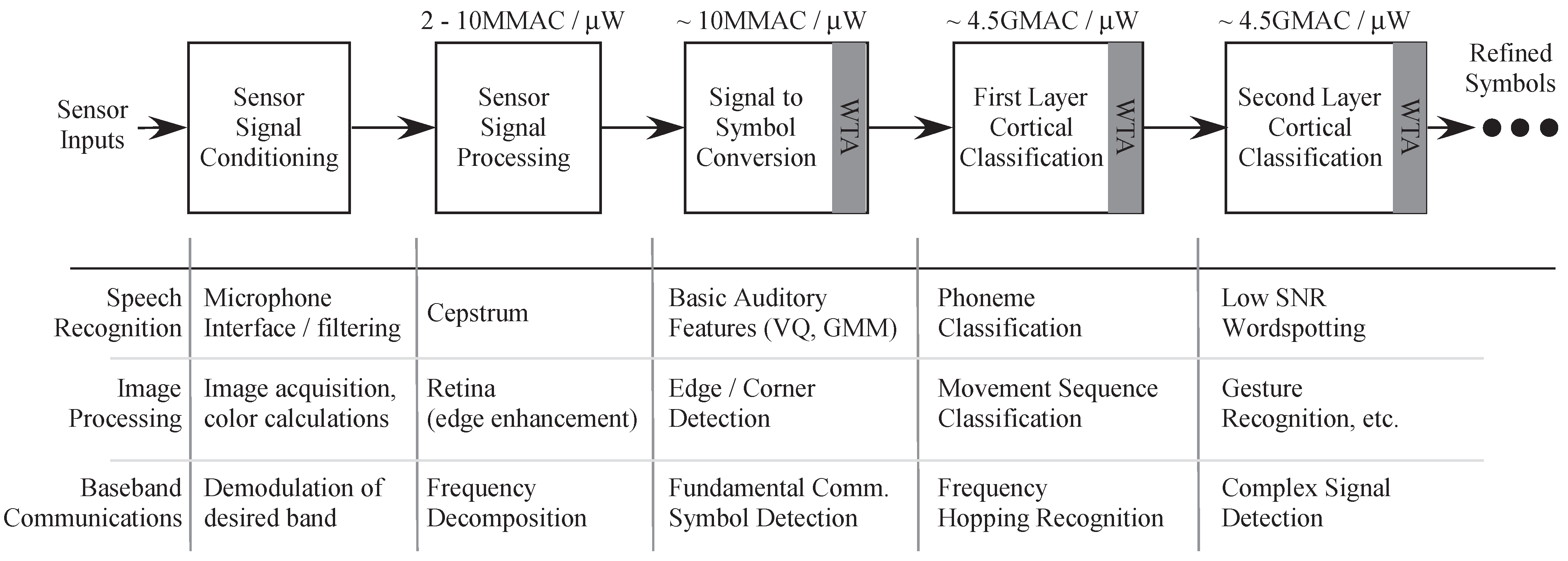
A typical Wordspotting system has at least three stages: Feature generation, Probability Generation (Signal to symbol conversion) and the State Decoding (classification) stage, which determines the word detected.
Figure 1b shows the general block diagram for a classification system. In the specific example of speech recognizer, the sensor would be a microphone stage. The first stage has interface circuitry to acquire the signal from the microphone as well as initial signal processing. This processing may include signal conditioning and filtering, frequency decomposition as well as signal enhancement.
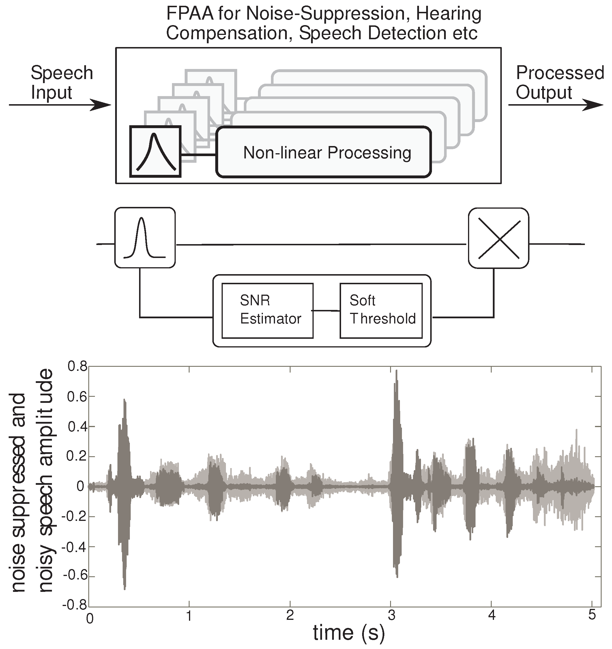
Figure 2 shows the FPAA as a prototyping device for audio signal processing applications. Our approach to audio processing includes a range of signal processing algorithms, that fit into the pathway between speech production (source) and perception (human ear). These algorithms are implemented by non-linear processing of sub-banded speech signals for applications such as noise suppression or hearing compensation, by proper choice of the non-linearity. In addition, the outputs of the non-linear processor can be taken at each sub-band, for speech detection instead of recombining to generate a perceptible signal for the human ear. Using this general framework, a variety of non-linear processing can result in applications in speech classifiers and hearing aid blocks. Here, we focus on the application of speech enhancement by noise-suppression, targeting word recognition in noisy environments. Detailed experimental results for a noise suppression application are discussed in [
9], where the speech-enhanced sub-band signals are recombined together. For a speech recognizer, we use the enhanced sub-band signals directly to extract basic auditory features.
Figure 2.
High level overview: The FPAA can be used for a variety of audio processing applications using the signal framework described. The first stage is a frequency decomposition stage followed by a non-linear processing block. The non-linear circuit can be used to implement the SNR estimator and a soft-threshold, which sets the gain in each sub-band. The gain control is implemented using a multiplier. Transient results from a MATLAB simulation of a 4 channel system is plotted. The noisy speech is gray, while the processed speech is in black.
The second stage of the speech classifier consists of the probability generation stage that detects basic auditory features and supplies input probabilities to the state decoding stage. These enhanced sub-band signals undergo first-level information refinement in the probability generation stage, resulting in a sparse “symbol” or “event” representation. This stage maybe implemented as an Artificial Neural network (ANN), Gaussian Mixture model (GMM) or a Vector Matrix Multiplier (VMM) + WTA classifier. A typical 2-layer NN has synaptic inputs represented by the VMM and the sigmoid modeling the soma of a point-neuron. Alternatively, we can have synaptic computation followed by a competitive network modeled by the WTA.
We show in [
10] that a single-stage VMM + WTA classifier can be used as a universal approximator, in contrast to an ANN implementation which requires two layers to implement a non-linear decision boundary.
Figure 3 shows the comparison in circuit complexity of a two-layer ANN and a VMM + WTA classifier. A 1-layer NN requires the computation of a Vector-Matrix Multiply (VMM) + neuron. The addition of various weighted inputs is achieved through Kirchhoff’s Current Law (KCL) at the soma node, adding all currents. The computation at the neuron is governed by the choice of complexity in the model. Usually, for moderate size of the network, the synaptic computation dominates the neuron computation. The sigmoidal threshold block for the soma nonlinearity in a NN can be implemented in voltage mode by converting the current output from the VMM into voltage and using a voltage-mode threshold block, or in current mode with an
block. Either of these implementations require more transistors per neuron compared to a WTA, which requires as few as 2 transistors per neuron.
Figure 3.
Basic auditory feature extraction and probability generation stage: The speech input undergoes frequency decomposition or enhancement resulting in sub-band signals. The probability generation block can be implemented using an ANN, GMM or the VMM + WTA classifier. The circuit complexity is halved by using a VMM + WTA classifier.
The VMM + WTA classifier topology has the advantage of being highly dense and low power. Each multiply is performed by one single transistor that stores the weight as well, and each WTA unit has only 2 transistors, providing very high circuit density. Custom analog VMMs have been shown to be 1000× more power efficient than commercial digital implementations [
11]. The non-volatile weights for the multiplier can be programmed allowing flexibility. The transistors performing multiplication are biased in deep sub-threshold regime of operation, resulting in high computing efficiency. We combine these advantages of VMMs with the reconfigurability offered by FPAA platforms to develop simple classifier structures.
In this paper, we demonstrate the state decoding stage of a simple YES/NO wordspotter. We have implemented an HMM classifier using bio-physically based CMOS dendrites for state decoding. For all experimental results in this paper, it is assumed that we have the outputs of the feature and probability generation stages.
We shall describe an HMM classifier model and its programmable IC implementation using CMOS dendrites. The first part of this paper describes the similarity between a single dendritic branch and HMM branch, in addition to exemplifying its usage to compute a metric for classification. An HMM classifier is modeled comprising of these dendritic branches, a Winner-Take-All (WTA) circuit and other supporting circuitry. Subsequently, the computational efficiency of this implementation in comparison to biological and digital systems is discussed. Intriguingly, this research substantiates the propensity of computational power that biological dendrites encompass, allowing speculation of several interesting possibilities and impacts on neuroscience. It is in some ways a virtual visit into the dendritic tree as was suggested by Segev
et al. [
12]. This paper further explores the interlinks between neurobiology, Hidden Markov Models and CMOS transistors based on which we can postulate that a large group of cortical cells function in a similar fashion as an HMM network [
4,
7]. Section II describes the similarities between a dendrite branch and an HMM branch. We discuss the similarities between a simulated HMM branch and experimental results using a CMOS dendrite branch. In Section III, we discuss the single CMOS dendrite in detail. We will present experimental results for the line for different parameters. We also discuss the simulation model that we have developed and the similar results seen. In section IV, we discuss the Analog HMM classifier implementation. We discuss the experimental results for a YES/NO wordspotter for different sequences. In section V, we discuss the tools that made the implementation of this classifier structure possible. In section VI, we will discuss the computational efficiency of the system as compared to digital and biological systems. In the final section we will summarize the results and discuss the future possibilities.
2. Dendritic Computation and the HMM Branch
For a typical HMM used for speech recognition, the update rule is given by:
The probability distribution
, represents the estimate of a symbol (short segment of speech/phoneme) produced by a state
i in frame
n.
represents the likelihood that a particular state, was the end-state in a path of states that models the input signals [
13] as shown in Equation (
1).
is the transition probability from one state to another. In a typical speech recognition model, the states would be phonemes/words and the output would represent the audio signal produced by the subject. The features of the audio signal tend to vary for different subjects. The goal of this classifier model is to correctly classify a sequence of symbols with some tolerance. For an HMM state machine for speech recognition using CMOS dendrites, the inputs
can be modeled as Gaussian inputs as shown in
Figure 4a, which is typical for
for speech signals with an exponential rise-time and fall-time. In
Figure 4b, the likelihood outputs for each state shows a very a sharp decay and has a very high dynamic range.
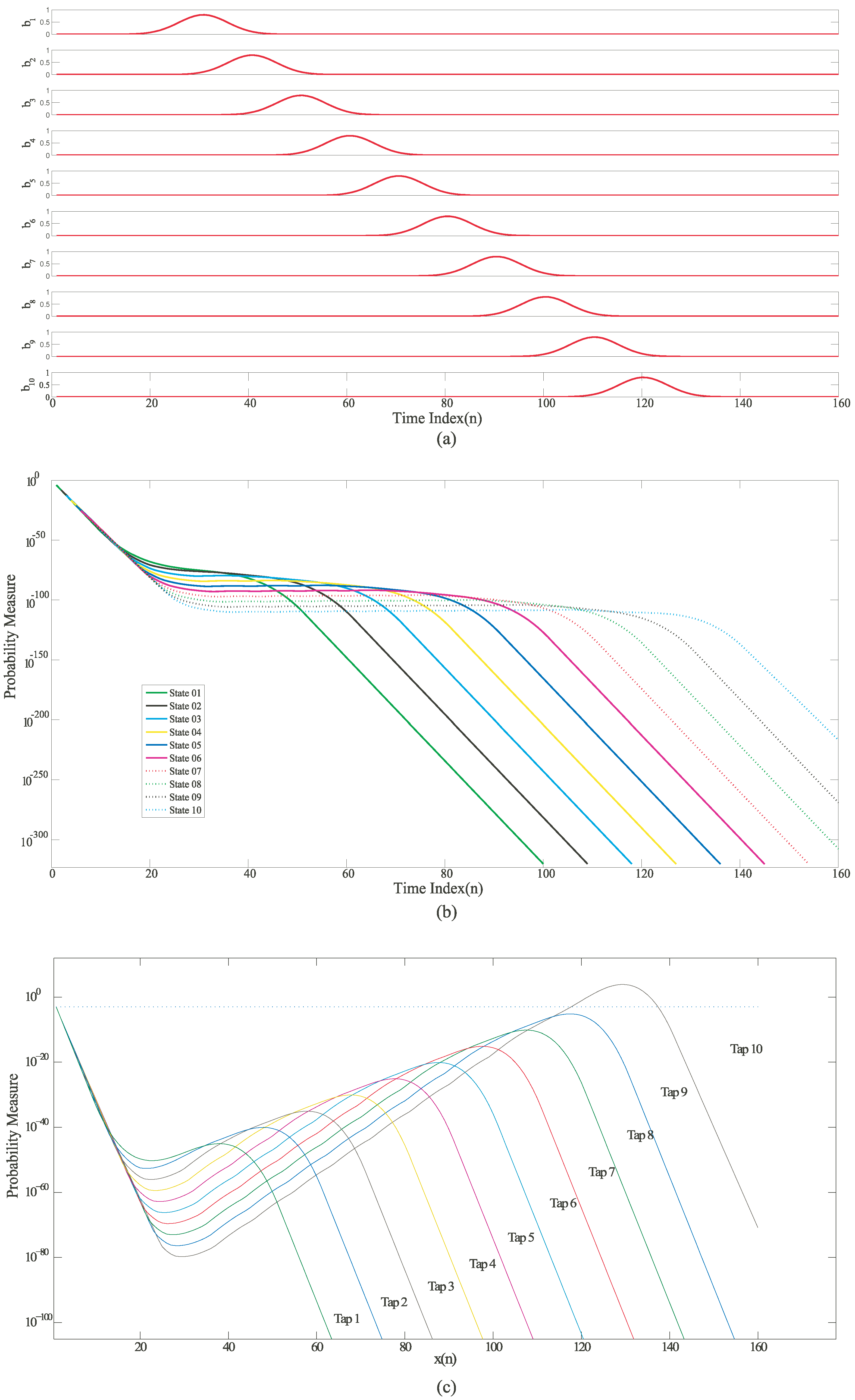
Figure 4.
Simulation results for an HMM state machine based on a Mathematical HMM model built using MATLAB (a) Input probability distribution of different symbols varying with time; (b) Likelihood outputs of all the states on a logarithmic scale; (c) Normalized likelihood outputs of all the states. The outputs were normalized by multiplying them with an exponential function of the form .
Figure 5.
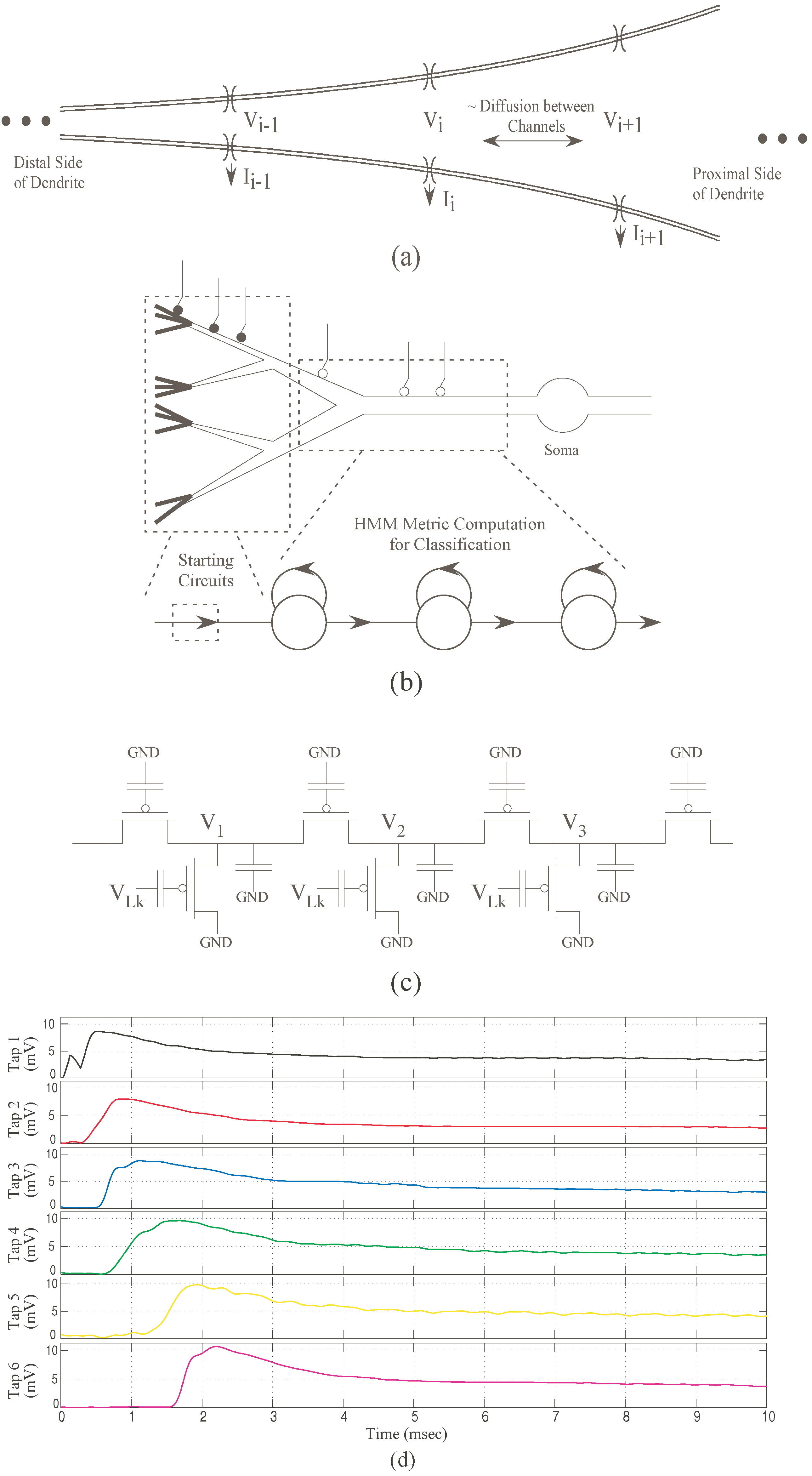
CMOS implementation for a dendritic branch and experimental results. (a) Dendrite with increasing diameter as typically seen in pyramidal cells. We refer this increasing diameter as “taper”; (b) Co-relation between basic left-to-right HMM branch and a CMOS dendrite branch with “taper”; (c) Resulting IC implementation using programmable analog floating-gate pFETs. For the CMOS dendrite the “taper” is modeled by increasing the axial conductance from left-to-right; (d) Experimental results showing the outputs from each tap of the CMOS dendrite. These outputs are equivalent to likelihood outputs from the HMM states. The output doesn’t decay completely but attains a new dc level. Note that we did not do normalization explicitly for the outputs of the dendrite as the decay is not as sharp as seen in HMMs. All taps are set initially to have the same membrane voltage .
Figure 5.
CMOS implementation for a dendritic branch and experimental results. (a) Dendrite with increasing diameter as typically seen in pyramidal cells. We refer this increasing diameter as “taper”; (b) Co-relation between basic left-to-right HMM branch and a CMOS dendrite branch with “taper”; (c) Resulting IC implementation using programmable analog floating-gate pFETs. For the CMOS dendrite the “taper” is modeled by increasing the axial conductance from left-to-right; (d) Experimental results showing the outputs from each tap of the CMOS dendrite. These outputs are equivalent to likelihood outputs from the HMM states. The output doesn’t decay completely but attains a new dc level. Note that we did not do normalization explicitly for the outputs of the dendrite as the decay is not as sharp as seen in HMMs. All taps are set initially to have the same membrane voltage .
To limit this range, we normalize this output with an exponential function. It can be observed that the normalized likelihood is similar to an EPSP signal with an asymmetric rise and fall time. For a single
n-stage dendritic line with “taper”, if we applied sequential EPSP inputs at subsequent nodes, the output observed at the end of the line is as shown in
Figure 5d. A “taper” signifies the changing diameter through the length of a dendrite. It represents the normalized likelihood outputs of an HMM classifier. The Gaussian inputs for the HMM model can be modeled using synaptic currents for a dendrite which is also typical for biological systems.
is thus represented as the synaptic current into each node. The output voltage of each tap of the dendrite represents the likelihood
of an HMM state. This can be linearly-encoded or log-encoded depending on the region of operation. For the dendritic system, no normalization is done as the decay is not as sharp as seen in the HMM branch for a wide dynamic range.
For a continuous-time version of Equation (
1), the update rule is given by,
where,
is the input probability of symbol in state
i; and
is the likelihood of a state
i at time
t;
τ is the time index between two consecutive time indexes and
is the transition probability between adjacent states. Even though the state sequence is implied, one cannot assume a definitive observation of transition between the states. This is the reason why it is called
Hidden Markov Model although the state sequence has a Markovian structure [
14]. Continuous-time HMMs can be represented as a continuous-time wave-propagating PDE as given in Equation (
3) [
15].
where, Δ is the distance between two state nodes. This can be compared to analog diffuser circuits. Also, an HMM branch and a dendrite branch have similar looking topologies and similar wave-propagating properties. The HMM state machine used, as shown in
Figure 4a, is a left-to-right model. Studies have shown that a biological dendrite also does not have a constant diameter [
16]. Its diameter at the distal end is smaller as compared to the proximal end as shown in
Figure 5a,b [
17]. Thus, for a similar CMOS dendritic line that is uni-directional, we would expect the axial conductances of the line to increase from left-to-right as shown in
Figure 5c. This is the case of a dendrite with “taper”. Such a topology ensures that the current flow is uni-directional. This also favors coincidence detection in the dendrite. We can compare the continuous-time HMM to an RC delay line with “taper”. For this let us analyze the behavior of an RC delay line with and without taper.
2.1. RC Delay Line without Taper
The classical RC delay line is reviewed in Mead’s text [
18].
Figure 6 shows the topology. Kirchhoff’s Current Law (KCL) can be used to derive a differential equation for this circuit, given by Equation (
4), where
G is conductance.
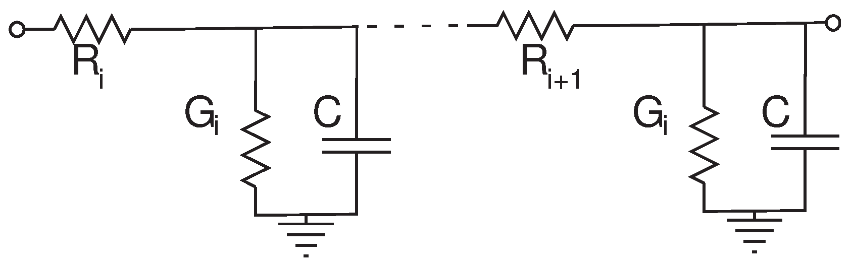
Figure 6.
RC delay line representing a dendrite. The Rs represent the axial resistances, the Gs represent the leakage conductances and C is the membrane capacitance.
Figure 6.
RC delay line representing a dendrite. The Rs represent the axial resistances, the Gs represent the leakage conductances and C is the membrane capacitance.
Assuming the horizontal resistances are equal as given in Equation (
5) allows one to simplify Equation (
4) to Equation (
6):
Assuming there are many nodes allows one to perform the following change of notation from discrete nodes to continuous nodes:
Assuming that
represents a “position delta” one may use the Taylor series to describe the continuous nodes in terms of
, Equations (10) and (11).
Substituting Equations (10) and (11) into Equation (
6) and simplifying, yields Equation (
12), the generalized PDE describing the RC delay line diffusor.
If one assumes no input current at the top of each node
, then one can put the diffusor circuit into a form similar to the continuous time HMM equation as given in Equation (
13).
The impulse response of such a system is a Gaussian decaying function over time. In this case, diffusion is the dominant behavior of the system.
2.2. RC Delay Line with Taper
Assuming that HMM will always propagate to the next state and there is no probability that it will remain in its current state leads to the assumption as given in Equation (
14) which can be substituted in Equation (
3):
For a dendrite circuit with taper, axial conductances are NOT equal and increase towards the right. Using this assumption, Equation (
4) simplifies to Equation (
15):
Substituting the Taylor series expansions of Equations (10) and (11) into the above we get:
Assuming that
we can neglect higher order terms of the Taylor series.
We can see in Equation (
16) that there is still some diffusion that can be seen in the line. It is however negligible as the wave propagation term is more dominant. Re-arranging terms and assuming no input current we get:
Table 1 closely examines the similarities between a RC delay line and an HMM PDE.
Table 1.
Comparing HMM PDE and RC Delay Line Terms w/Assumptions.
Table 1.
Comparing HMM PDE and RC Delay Line Terms w/Assumptions.
| Element description | HMM PDE | RC delay line |
|---|
| Recursion variable | | |
| State element coefficient | τ | |
| Decay term coefficient | | |
| Wave propagation/diffusion term | | |
3. Single Line CMOS Dendrite
Since dendrites have computational significance, it is interesting to explore computational models that can be built using dendrites or a network of dendrites. One such application is classification in speech recognition. We have already discussed the similarities between an HMM branch and a dendritic branch. To test this hypotheses, we implemented a single dendritic branch with spatially temporal synaptic inputs. We compared a single CMOS dendritic branch implemented on a reconfigurable analog platform and a MATLAB Simulink simulation model based on the device physics of CMOS transistors.
Figure 7 shows a complete overview of how CMOS dendrites are modeled and also the experimental results for a 6-compartment CMOS dendrite. The inputs to the dendrite are synaptic currents. In biological systems, synaptic inputs can be excitatory and inhibitory in nature. However, in this paper we assume that we have excitatory synapses as a majority of contacts on a pyramidal cell are excitatory in nature. As discussed before the dendrite does not have a constant diameter. This implies that for a CMOS dendrite, the conductance of the dendrite increases towards the soma
i.e., from left to right [
17]. The inputs will also decrease in amplitude as conductance increases. This ensures that an input closer to the soma does not have a larger effect than inputs farther away. This indicates decreasing synaptic strengths of inputs down the dendritic line. This has been observed previously in biological dendrites [
16]. Thus, we also varied the synaptic strengths of inputs in our experiments. We implemented the single dendritic line both as a CMOS circuit model and a MATLAB Simulink simulation model. We found that the comparison of our experimental and simulation results were fairly close. This is demonstrated in
Figure 8.
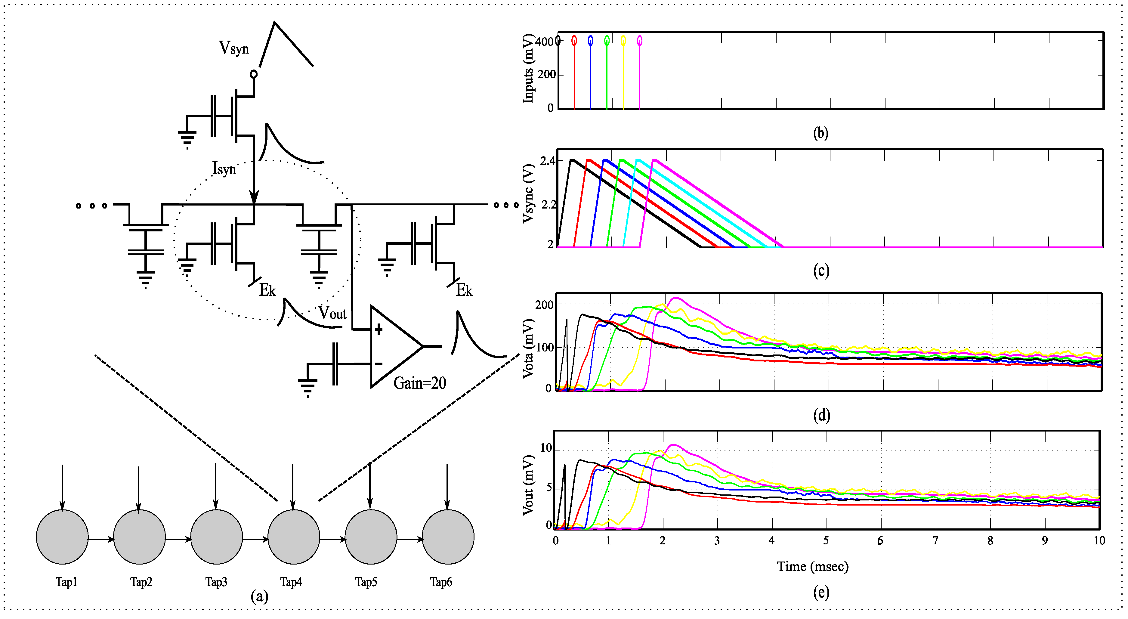
Figure 7.
System overview for a dendrite branch. (a) Detailed diagram for a single dendritic line which is equivalent to an HMM branch; (b) The representation of input voltage on the source of the transistor representing the input synapses; (c) The asymmetric triangular input voltages on the source of the transistor representing the input synapses. , the input synapse currents into each of the different nodes is proportional to ; (d) , the output of FG-OTA which has a gain of approximately 20; (e) , the output voltage at each node.
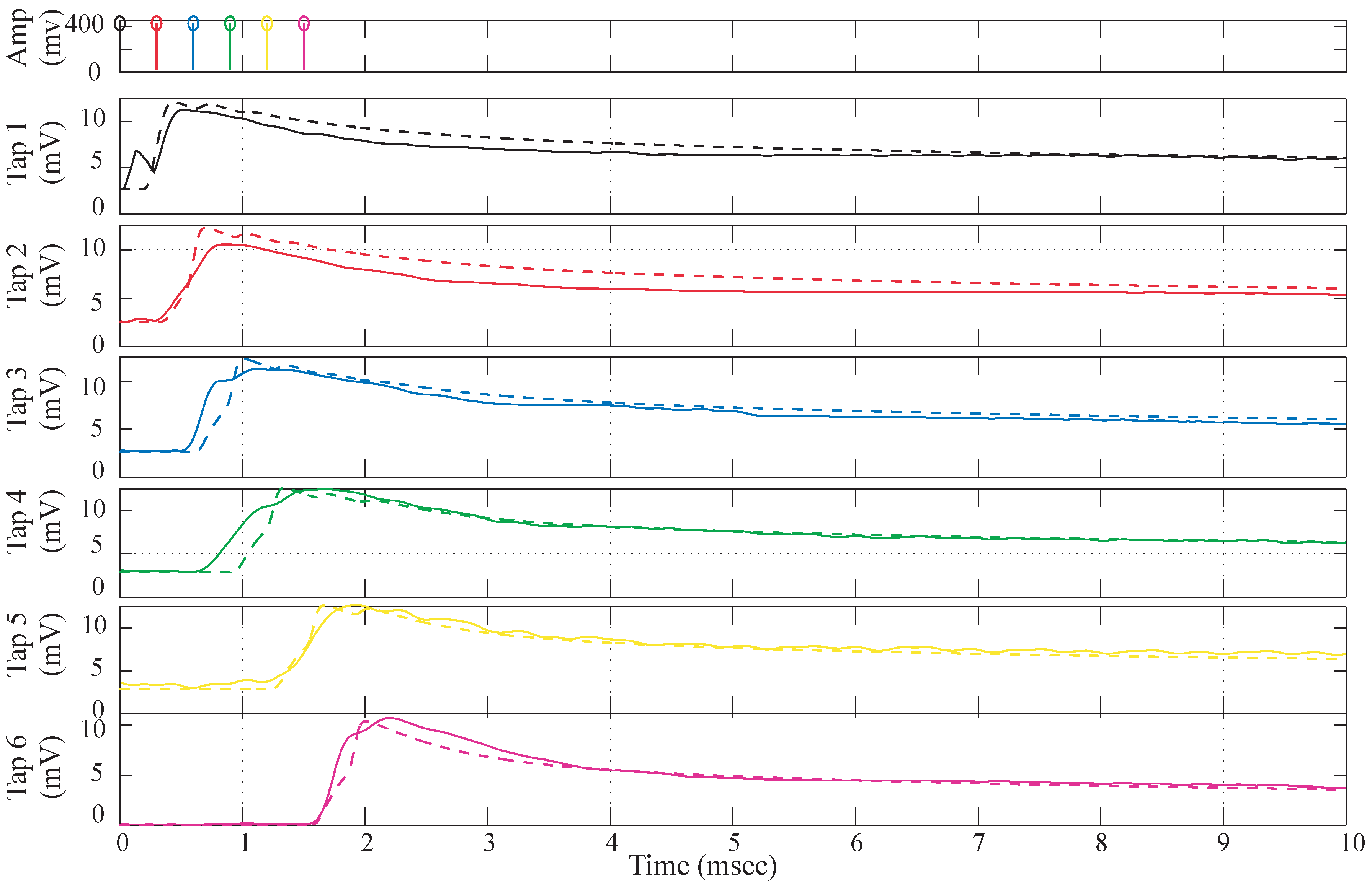
Figure 8.
Simulation Data vs. experimental data comparison. The dotted lines depict the simulation data and the solid lines are the experimental data. The parameters for simulation data are , , , , , , .
Figure 8.
Simulation Data vs. experimental data comparison. The dotted lines depict the simulation data and the solid lines are the experimental data. The parameters for simulation data are , , , , , , .
3.1. Inputs to the PFET Source
The input probabilities
are represented as log-compressed voltage signal at the dendrite node. To generate EPSP input currents into each of the dendritic nodes, we input an asymmetric triangular wave voltage at the source of the pFET FG-FETs. This generates typical EPSP signals, which have a faster rising time and a slower fall time. By varying the magnitude of the triangular waves we were able to control the input current into each of the nodes of the dendrite. This can be seen in
Figure 7c. The current of a transistor is exponentially proportional to its source voltage
.
where,
. This enables us to generate EPSP-like inputs for the CMOS dendrite. All input representations shown thus are voltage inputs on the source of the transistor, that acts as synapse at every node of the dendrite.
3.2. Single Line Dendrite Results
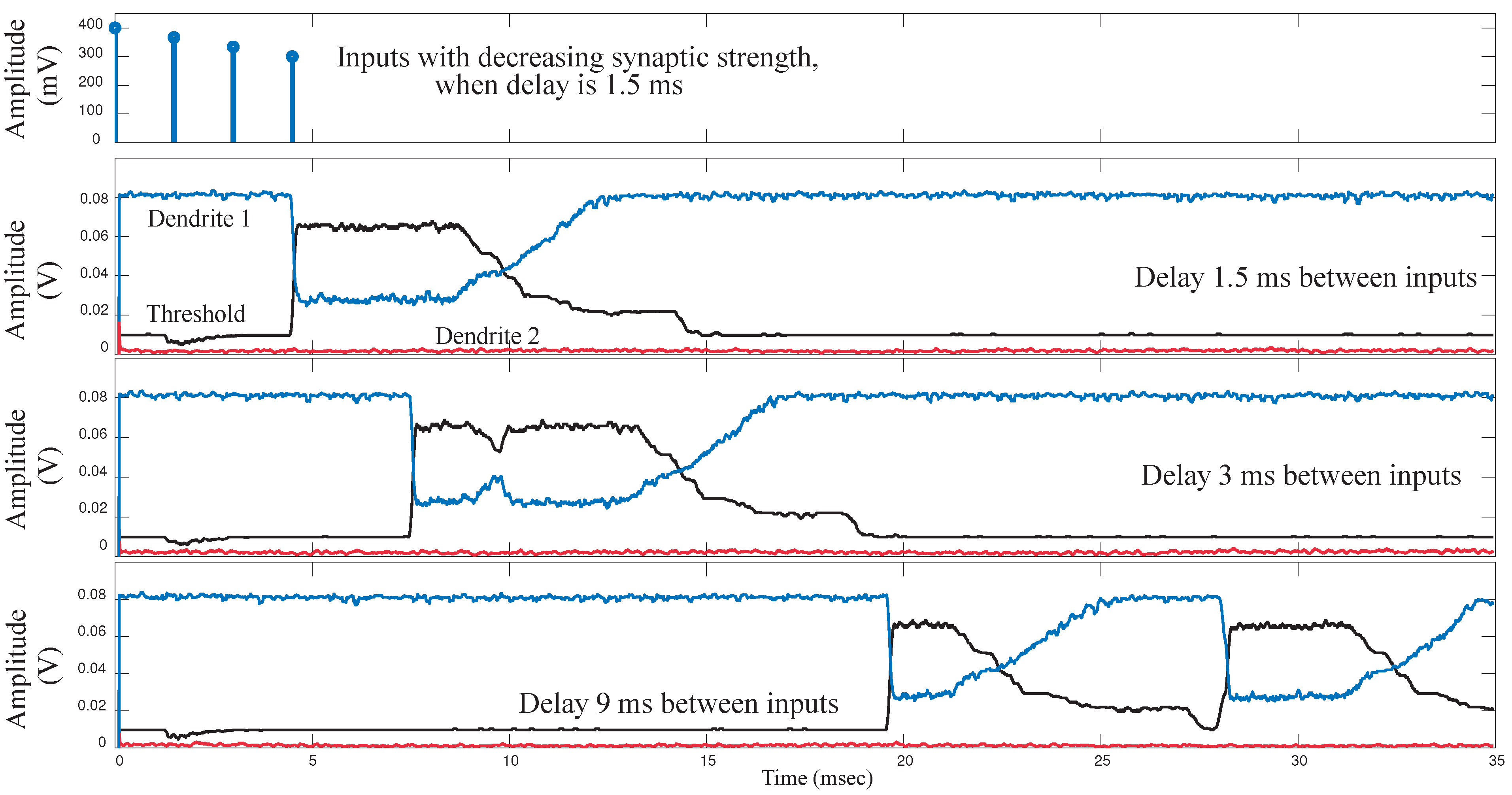
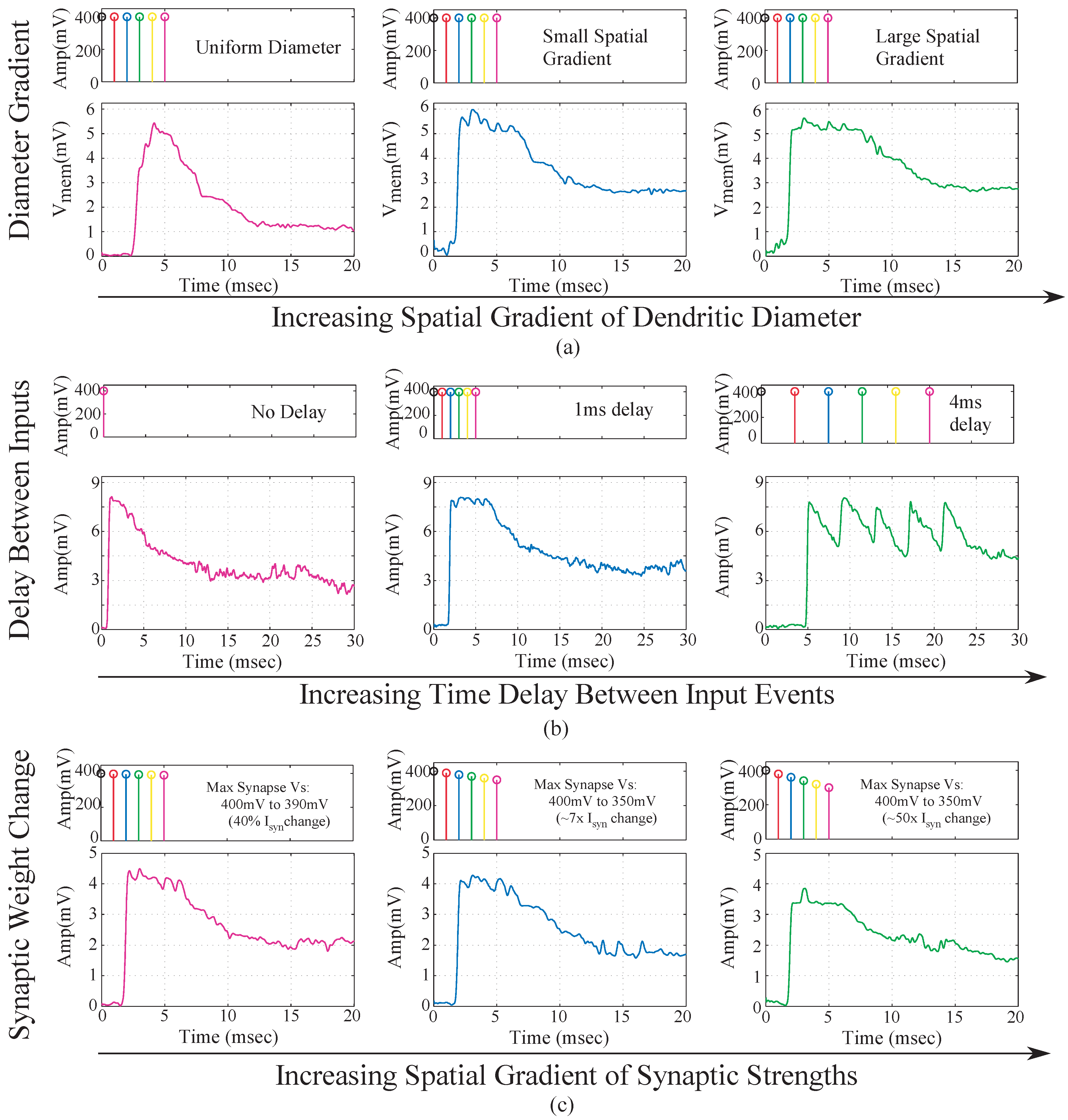
We implemented a single 6-compartment dendrite. Each compartment consisted of 3 FG pFETS for the axial conductance, the leakage conductance and the synaptic input respectively. We present experimental results for the same. To test the behavior of dendrites for a typical speech model, we varied three parameters namely: “taper”, delay between inputs and the EPSP strengths of the synaptic inputs. In terms of “taper”, two approaches were tested. One without “taper” and the second with increasing “taper”. Results are shown in
Figure 9a. We observed that by using “taper” we could ensure that the input current would transmit more in one direction of the dendritic cable. To achieve this we increased the axial conductance of the cable down the line, such that maximum current tends to flow to the end of the cable. At every node of the dendrites we input EPSP currents in a sequence. This is similar to a speech processing model, where all the phonemes/words are in a sequence and based on the sequence we classify the word/phoneme. We then varied the delay between the input EPSP signals as seen in
Figure 9b. It was observed that as the delay between the inputs increases, the amplitude of the output decreases. This implies that as outputs are spaced farther apart, there is less coincidence detection. The third parameter varied was the strength of the EPSP inputs, with the difference in EPSP strengths of the first node and the last node increasing for subsequent plots as seen in
Figure 9c. The EPSP strengths near the distal end are larger than the EPSP strengths near the proximal end. Evidence for the same has been shown in biology [
16]. It was observed that as the difference in amplitude was increased, the amplitude of the output reduced. The study of the variation of these parameters showed the robustness that such a system would demonstrate in terms of speech signals. The difference in delay, models the different time delays between voice signals when a word is spoken by different subjects. The difference in EPSP strengths ensures that the impact of all the phonemes on the output is similar for detection of a word and not dominated by just the last stage.
In
Figure 10, we have studied the trends that one would observe collectively for different parameters. The output metric here is the difference of amplitude of last node when all inputs are present and when only the last input is present. We observed that as we increased the timing difference between various inputs, the final metric of the line decreased as seen in
Figure 10b. We simulated the dendritic branch to observe the effects a wide range of time delays between inputs as shown in
Figure 10c. We observed that the output metric decreased as we increased the delay between the inputs for a line. And for the cases where we reversed the sequence, the amplitude was very close to zero. This clearly demonstrates that if the sequence of the inputs is not in succession, there will be no word detection. Also, the output metric decreases as the delay between the inputs increases.
Figure 9.
Experimental results for a single branch 6-tap dendrite for different parameters. The three main parameters that govern the output of a dendrite are, namely the taper of the line, the spatial-temporal characteristics of the synaptic inputs and the strength of the synaptic inputs. All results are from the last tap of the dendrite. (a) Metric changed is the taper of the dendrite. For subsequent figures, the taper is increased from no taper to a larger taper. The diameter of the dendrite increases down the line which is achieved by increasing the conductances of the axial transistors from left to right; (b) Metric changed is the delay between EPSP inputs into each of the taps of the dendrite. In the first case we have zero time unit delay, 10 time units delay for second and 20 time units delay for the third diagram in the sequence. One time unit = ; (c) Metric changes is the difference between the EPSP strengths of the input signals. In the first case, the difference is 10 mV, 50 mV for the second and 100 mV for the third case. As can be seen in the graph we can see decreasing amplitude as the difference in EPSP strengths increases
![Jlpea 03 00073 g009]()
Figure 10.
Experimental results, simulation results and trends observed for a single line dendrite. We varied the input sequence with respect to the time difference between signals. The output metric in this case is the difference between the output of the dendrite when all signals were present and output of the dendrite when only the last input was present. (a) Diagram depicting the decreasing EPSP inputs into a single CMOS dendrite line; (b) Experimental data showing change in peak to peak amplitude for a dendrite as the EPSP inputs into each of the nodes decrease down the line; (c) Change in amplitude of the output with respect to increasing difference in the EPSP amplitudes as we progress from left to right down the line. implies the time delay between inputs. As we increase the time delay the output metric reduces. Negative implies a reversed sequence of inputs, where the output metric is zero; (d) Change in amplitude of the output with respect to increasing difference in the taper of the dendrite. In this experiment, the diameter of the dendrite was increased as we progress from left to right down the line. implies the time delay between inputs. As we increase the time delay the output metric reduces. Negative implies a reversed sequence of inputs, where the output metric is zero. The study of these parameters showed the robustness that such a system would demonstrate in terms of speech signals. The difference in delay, models the different time delays between voice signals when a word is spoken by different people. The difference in EPSP strengths ensures that the impact of all the phonemes on the output is similar for detection of a word and not dominated by just the last stage.
![Jlpea 03 00073 g010]()
4. Analog Classifier for Word-Spotting
We will now discuss the complete classifier structure. We have built a simple YES/NO HMM classifier using dendrite branches, a Winner-Take-All (WTA) circuit and supporting circuitry. We will simplify the modeling of a group of neuron somas and the inhibitory inter-neurons as a basic WTA block, with one winning element. We can consider the winning WTA output, when it transitions to a winning response as an equivalent of an output event (or action potential). To build this network, we made a model of a dendrite, initially a single piece of cable with branch points, where the conductance of the line gets larger towards the soma end, and the inputs are excitatory synaptic inputs. For classification, we focus on the ability for dendritic trees to be able to compute useful metrics of confidence of a particular symbol occurring at a particular time. This confidence metric will not only be a metric of the strength of the inputs, but also will capture the coincidence of the timing of the inputs. We would expect to get a higher metric if the
,
, and
, inputs arrived in sequence, whereas we would expect a lower metric for the
,
, and
inputs arrived in sequence. This type of metric building is typical of HMM type networks. Simple example being if the word “Y” “E” “S” were detected in a sequence as opposed to “S” “E” “Y”. This is demonstrated by the simulation results as shown in
Figure 10, where when the input sequence is reversed the output metric is zero. The output metric is defined as the difference in output of last node when all inputs are present and when only the last input is present.
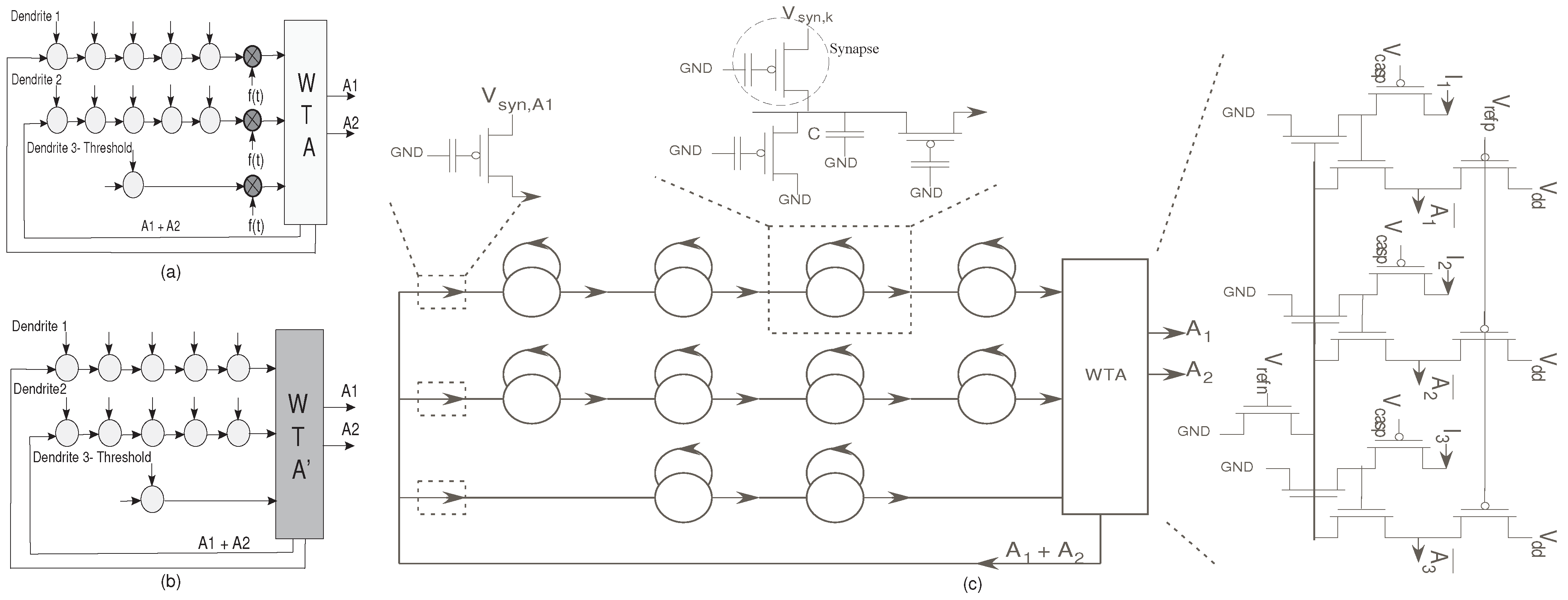
Figure 11.
(
a) The classifier structure with the normalization factor multiplied,
; (
b) The classifier structure after normalization. This figure demonstrates that the normalization is inherent in the system; (
c) Detailed structure of the HMM classifier using reconfigurable floating-gate devices. There are three main structures here : The dendrite branches, the Winner-Take-All circuit and the supporting circuitry. The dendrite branch consists of a 5-stage dendrite for both the branches representing the words YES and NO; and a single stage dendrite to set the the threshold current. The dendrites have synaptic inputs at each node, which represent the phonemes of the word to be detected. When the output of a dendrite exceeds the threshold limit
i.e., if a YES/NO is detected, the threshold loses. The supporting circuitry consists of a Vector-Matrix Multiplier (VMM) building block which acts as a reset after a word is spotted [
11].
The network we built has two desired winning symbols, “YES” and “NO”. Each symbol is represented by one or more states that indicate if a valid metric has been classified. Only the winning states would be seen as useful outputs. The useful outputs feed back to the input dendrite lines, and in effect reset the metric computations. This is implemented using a Vector-Matrix-Multiplier block [
11]. The system block diagram is as shown in
Figure 11. Each of the dendritic lines for the desired winning symbols has 5 states (dendritic compartments), where the inputs to the dendritic line represent typical excitatory synaptic inputs.
4.1. Synaptic Inputs Model Symbol Probability
In speech/pattern recognition, signal statistics/features are the inputs to the HMM state decoder. It generates the probability of the occurrence of any of the speech symbols. These signals when grouped, generate a larger set of symbols like phonemes or words [
13]. We assume we have these input probabilities to begin with, as inputs to the classifier structure. We have taken inspiration from Lazzaro’s Analog wordspotter for classification. However, we use a different normalization technique to eliminate the decay as shown in
Figure 4c. We can draw comparisons for such a system to a biological dendrite with synaptic inputs. We have modeled the input signals as excitatory synaptic currents. The synaptic current is given by :
Considering that
is the normalizing factor we have,
where,
is the system output before normalization. From Equations (21) and (24), we see that the input is similar to a synaptic current. Thus the inputs for the classifier using dendrites can be modeled as synaptic currents. This is represented in
Figure 11a and
Figure 11b. The derivation has two implications. First, we can use EPSP inputs to represent the input probabilities for phonemes. Second the system inherently normalizes the outputs. In
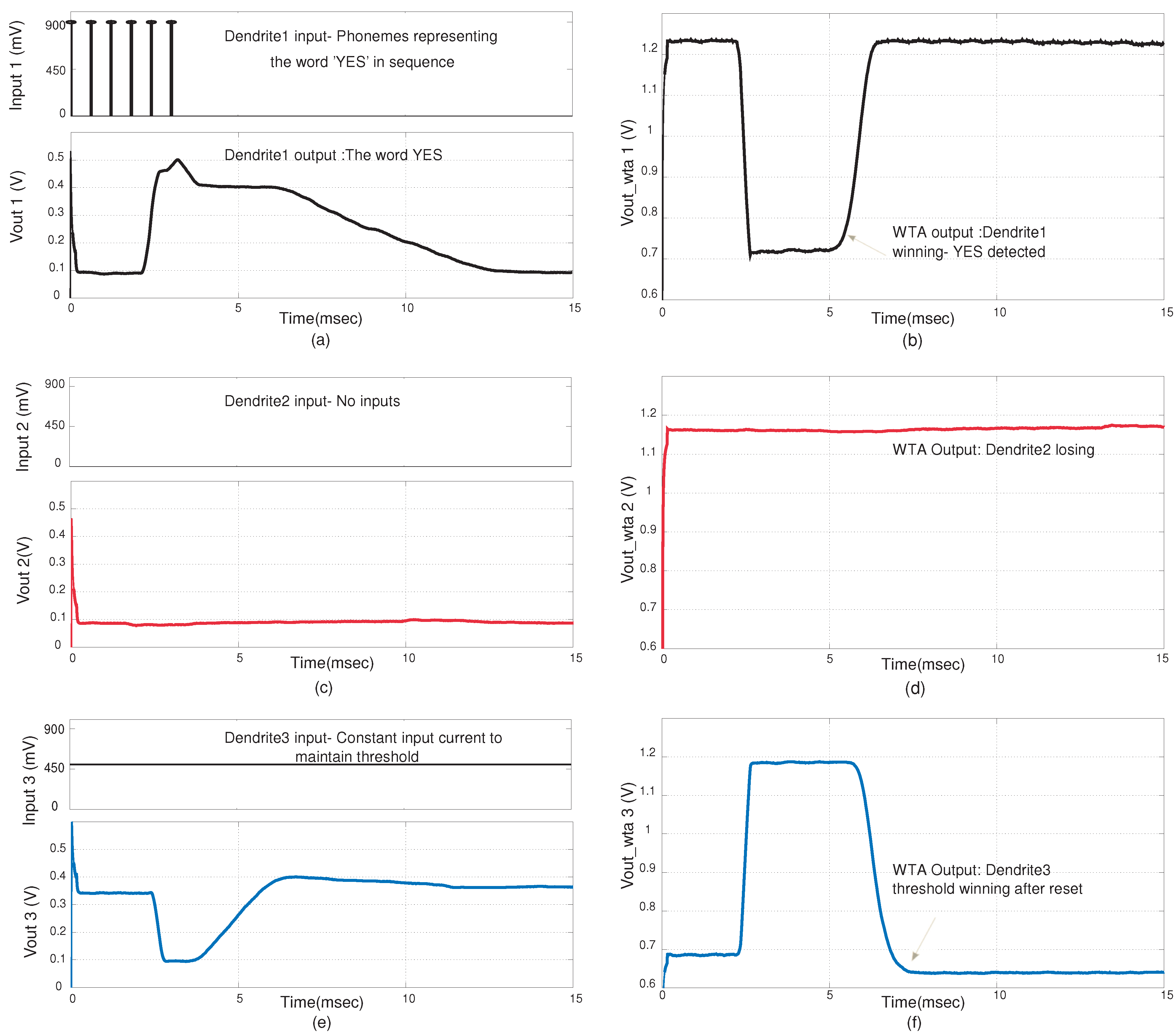
Figure 12, the input to dendrite-1 signifies the phonemes of the word “YES”. The inputs used were EPSP inputs that are similar to probability inputs
that in a typical HMM classification structure would be generated by a probability estimation block. There is no input into dendrite-2 which signifies that phonemes of “NO” were not detected. The threshold dendrite, dendrite-3 sets the threshold level. The WTA circuit determines the winner amongst the three dendritic lines. It is observed that when “YES” is detected, dendrite-1 wins. This happens when coincidence detection is observed at the output of dendrite-1. The winning line signifies the word that is classified. It is only when all the inputs are in sequence and cross the given threshold that the dendrite line wins. In
Figure 12 we demonstrate the classification of the word “YES”. The feedback from the WTA acts as a reset function for the dendrites, as after a word has been classified the threshold dendrite wins again. In
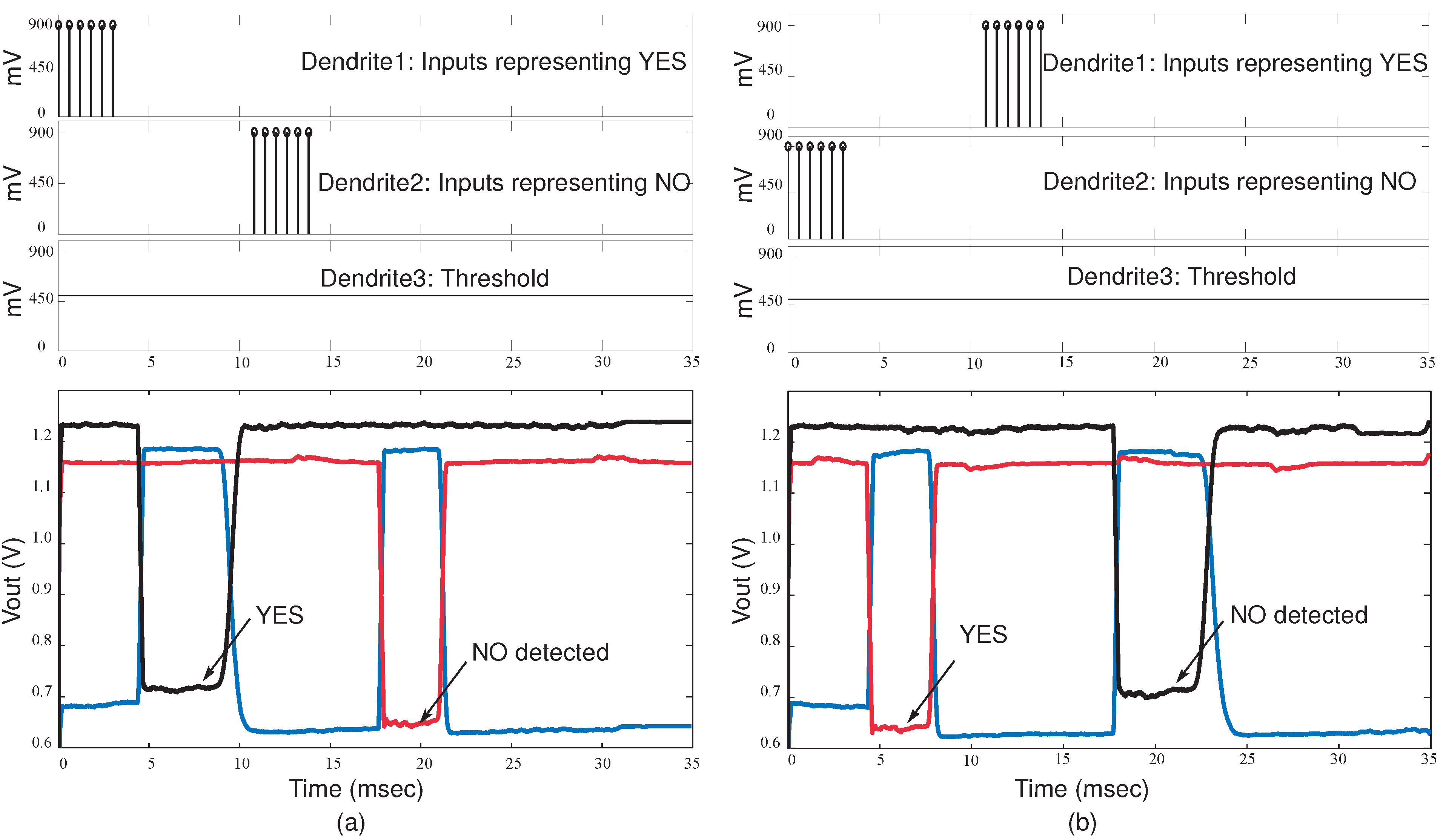
Figure 13, the classification of words “YES” and “NO” in a sequence is demonstrated. In
Figure 14 we show the effect of timing and variation of EPSP strengths for input sequences.
Figure 12.
Experimental results for the YES/NO classifier system. The results shown are for the case when a YES is detected by the system (a) Synaptic inputs at the nodes of the first dendrite and the line output for the first dendrite. Here we assume we have the input probability estimate for the phonemes (symbols) for the word YES; (b) Corresponding WTA output for first dendrite. A low value signifies that it is winning; (c) The synaptic input and output for the second dendrite; (d) Corresponding WTA output for the second dendrite; (e) The line output for the third dendrite; (f) Corresponding WTA output of the third dendrite. The third dendrite acts as a threshold parameter. The amplitude of the word detected on a particular line needs to be higher than the threshold to win.
Figure 13.
Experimental results for the classifier system when a sequence of words is detected. (a) First dendrite wins when the word YES is detected and the second dendrite wins when the word NO is detected. The WTA inputs and outputs are shown; (b) Second dendrite wins when the word NO is detected and first dendrite wins when YES in detected.
Figure 14.
Experimental results for the classifier system with different timing delays for inputs and varying synaptic strength. It demonstrates the effect of different timing in sequences. This implementation is for a classifier system with 4-tap dendrites, 3-input WTA and supporting circuitry. The WTA outputs for varying delays between inputs is shown. The delay between subsequent inputs is , and respectively. Also the inputs have different EPSP current strengths.
The winning output of the WTA is akin to an action potential. In terms of classification too, the WTA output signifies if a “word” has been detected. Our results have demonstrated that, such a system looks similar to an HMM state machine for a word/pattern. We can postulate from these experimental results that there are some similarities in computation done by HMM networks and a network of dendrites. The results are shown in
Figure 12 for a single word and for continuous detection of words in
Figure 13. We have demonstrated a biological model, built using circuits that is much closer than the implementation of any HMM network to date. Thus we have shown that an HMM classifier is possible using dendrites, and we have made a clearly neuromorphic connection to computation, a computation more rich than previously expected by dendritic structures.
6. Classifier: Computational Efficiency
Current approaches for Automatic Speech Recognition (ASR) use Hidden Markov Models as acoustic models for sub-word/word recognition and N-gram models for language models for words/word-class recognition. For HMMs, discriminative training methods have been found to perform better than other Maximum Likelihood methods like Baum-Welch estimation [
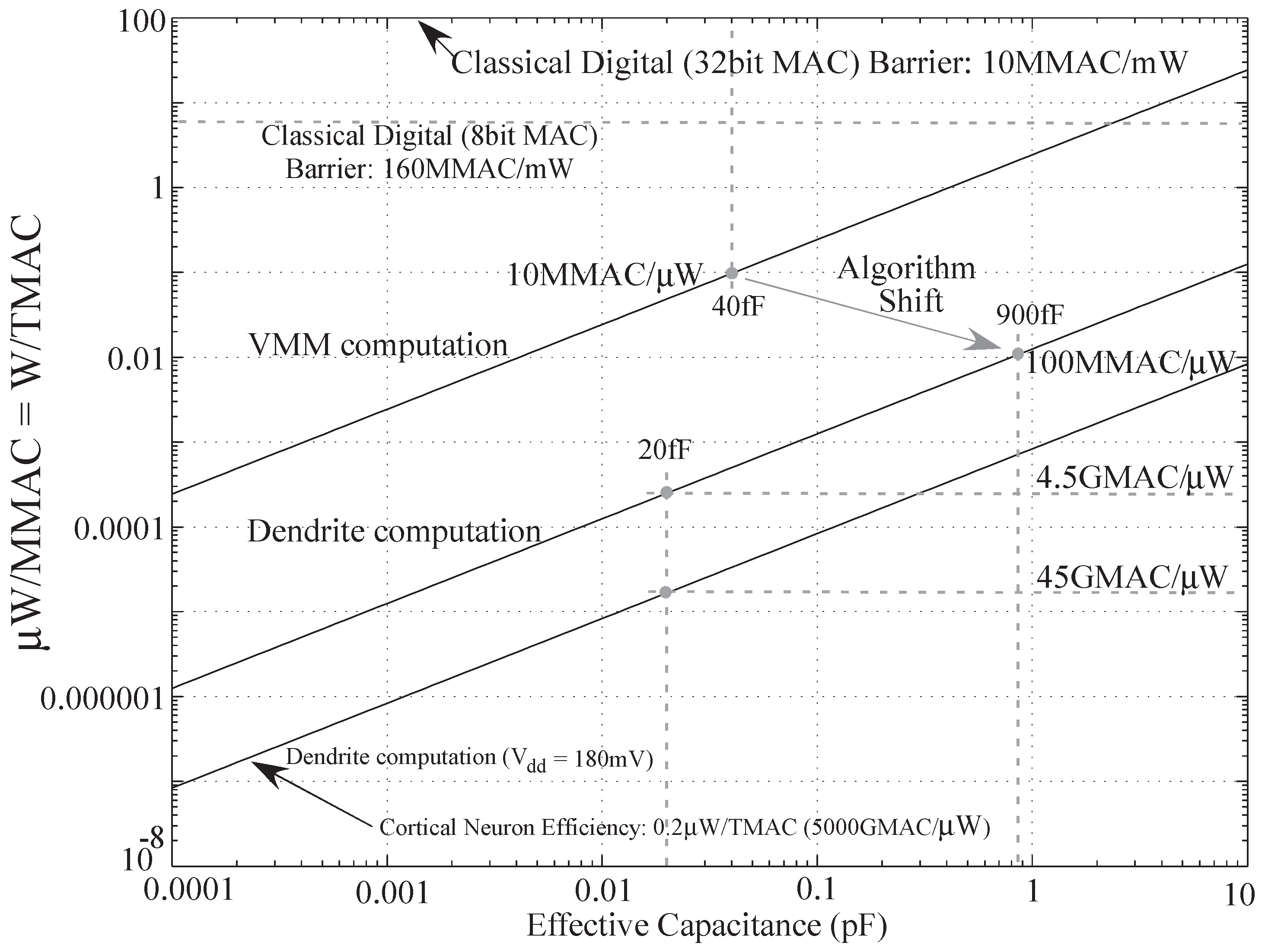
22] . Our dendritic model is similar to a continuous-time HMM model and can be used to classify sub-phoneme, phonemes or words. Typically, phoneme recognition models have a much higher error rate as they are much less constrained as compared to word recognition models. Based on our comparison studies for different features we hypothesize that our model would have higher tolerance levels and dynamic range. We have not used an audio-dataset to characterize our system, rather we have used symbolic representations to make a hypothesis. These are experiments we plan to do int he near future. However, we can compare the computational efficiency of these methods since we can model these systems mathematically. The unit used to compare computational efficiency is Multiply ACcumulates (MAC) per Watt. The energy efficiency at a given node of the system, depends on the bias currents, supply voltage and also the node capacitance.
We know that the node capacitance
C is the product of conductance and the time constant
τ. Now the bias current
for a dendrite node is given by,
where,
is the resting potential;
signifies the voltage of a potassium channel and G is the axial conductance. Also, power is the product of voltage across the node and current into the node. Now for a single node of an HMM classifier, we have 2 MAC/sample. Assuming
, which at a given node is approximately
. Thus,
We have compared the computational efficiency of digital, analog and biological systems as shown in
Table 2. Now for a wordspotting passive dendritic structure, we have 2 MAC/node. Typical dendrite would have over 1000 state variable equivalents in its continuous structure. For a particular neuron time constant
τ, we would want to have multiple samples for proper operation. For this discussion, let’s assume an effective discrete time sample rate 5 times more than
τ. Let us choose
for this discussion. Thus, we have each tree computing 10 MMAC for an HMM computation. For biological systems, say the brain has
neurons and total power consumption of about 20 W. Thus the power consumption is
pW/neuron. In a passive dendritic structure, the computational efficiency is 10 MMAC /neuron. Thus the computational efficiency of biological systems works out to be
MMAC/pW. Also from the equation it is evident that a major factor contributing to energy efficiency is node capacitance. Currently the node capacitance on the chip we used was
. If we further scale down the process used, this number will also reduce. This effectively means higher computational efficiency. A decrease to
itself will give us an improvement of 2 orders of magnitude. This is depicted in
Figure 15.
Table 2.
Comparing computational efficiency of Digital, Analog and Biological systems.
Table 2.
Comparing computational efficiency of Digital, Analog and Biological systems.
| Computing type | Computational efficiency |
|---|
| Digital (DSP) | MMAC/mW [23] |
| Analog SP (VMM) | 10MMAC/μW [11,24] |
| Analog (wordspotter) | MMAC/μW |
| Neural process | MMAC/pW |
Figure 15.
Computational efficiency
versus capacitance plot for VMM (analog) and dendritic computation algorithms for
[
25].
Figure 15.
Computational efficiency
versus capacitance plot for VMM (analog) and dendritic computation algorithms for
[
25].
7. Conclusions
We have demonstrated a low-power dendritic computational classifier model to implement the state decoding block of a YES/NO wordspotter. We have also found that this implementation is computationally efficient. We have demonstrated a single dendritic line with 6 compartments, with each compartment having a single synaptic input current. We have seen the behavior of a single dendrite line by varying three parameters, namely, the “taper”, the delay between inputs and the strength of the EPSP input currents. The effects of taper which enabled coincidence detection were studied. We have also seen the functioning of the WTA block with dendritic inputs and the how feedback helps initiate the reset after a word/phoneme is detected. We also build a Simulink dendritic model and simulated the output for time-varying inputs to compare with experimental data. This demonstrated how such a network would behave if inputs were in a sequence or if they were reversed.
The broader impact of such a system is two-fold. First, this system is an example of a computational model using bio-inspired circuits. Secondly the system proposes a computationally efficient solution for speech-recognition systems using analog VLSI systems. As we scale down the process, we can get more efficient and denser systems. We can also address how synaptic learning can be implemented and classification systems be trained. We can also model the input synapses as NMDA synapses to get a more multiplicative effect. In NMDA synapses, the synaptic strength is proportional to the membrane voltage. It couples the membrane potential to the cellular output. This could lead to a more robust system and is also closer to how biological systems are modeled. Also, we have modeled passive dendrites in this paper. It would be interesting to see how the system behaves when we add active channels. We currently have systems built that will enable us to further explore this discussion which is beyond the scope of this paper. There is a lot of scope for discussing how to build larger systems using this architecture. We can use spiking WTA networks for a larger dictionary of words. It is evident from the computational efficiency discussions, that clearly analog systems are a better choice for higher computational efficiency and lower costs. This calls for greater effort to build such systems. Reconfigurable/programmable analog systems open a wide range of possibilities in demonstrating biological processing and also for signal processing problems. As shown in
Figure 16 there is great potential in other areas as image processing and communication networks as well. These systems will not only enhance our understanding of biological processes but also will help us design more computationally efficient systems.
Figure 16.
Different applications using the Pattern Recognition system based on biology. It has application in speech and image processing and in communication systems. The state decoder in this paper is one block that is part of the whole system level design that we plan to build.
Figure 16.
Different applications using the Pattern Recognition system based on biology. It has application in speech and image processing and in communication systems. The state decoder in this paper is one block that is part of the whole system level design that we plan to build.


