Article

VLSI Architecture for 8-Point AI-based Arai DCT having Low Area-Time Complexity and Power at Improved Accuracy

by
Amila Edirisuriya
1,
Arjuna Madanayake
1,2,*,
Vassil S. Dimitrov
2,
Renato J. Cintra
3 and
Jithra Adikari
4
1
Department of Electrical and Computer Engineering, University of Akron, Akron, OH 44325, USA
2
Department of Electrical and Computer Engineering, University of Calgary, Calgary, AB T2N 1N4, Canada
3
Department of Statistics, Federal University of Pernambuco, Recife, PE 50740-540, Brazil
4
Department of Electrical and Computer Engineering, University of Waterloo, ON N2L 3G1, Canada
*
Author to whom correspondence should be addressed.
J. Low Power Electron. Appl. 2012, 2(2), 127-142; https://doi.org/10.3390/jlpea2020127
Submission received: 31 December 2011 / Revised: 22 March 2012 / Accepted: 26 March 2012 / Published: 29 March 2012
(This article belongs to the Special Issue Low Power Electronics - Recent Developments)

Abstract

:
A low complexity digital VLSI architecture for the computation of an algebraic integer (AI) based 8-point Arai DCT algorithm is proposed. AI encoding schemes for exact representation of the Arai DCT transform based on a particularly sparse 2-D AI representation is reviewed, leading to the proposed novel architecture based on a new final reconstruction step (FRS) having lower complexity and higher accuracy compared to the state-of-the-art. This FRS is based on an optimization derived from expansion factors that leads to small integer constant-coefficient multiplications, which are realized with common sub-expression elimination (CSE) and Booth encoding. The reference circuit [1] as well as the proposed architectures for two expansion factors α = 4.5958 and α = 167.2309 are implemented. The proposed circuits show 150 % and 300 % improvements in the number of DCT coefficients having error ≤ 0.1% compared to [1]. The three designs were realized using both 40 nm CMOS Xilinx Virtex-6 FPGAs and synthesized using 65 nm CMOS general purpose standard cells from TSMC. Post synthesis timing analysis of 65 nm CMOS realizations at 900 mV for all three designs of the 8-point DCT core for 8-bit inputs show potential real-time operation at 2.083 GHz clock frequency leading to a combined throughput of 2.083 billion 8-point Arai DCTs per second. The expansion-factor designs show a 43% reduction in area ( A ) and 29% reduction in dynamic power ( P D ) for FPGA realizations. An 11% reduction in area is observed for the ASIC design for α = 4.5958 for an 8% reduction in total power ( P T ) . Our second ASIC design having α = 167.2309 shows marginal improvements in area and power compared to our reference design but at significantly better accuracy.

1. Introduction

The 8-point discrete cosine transform (DCT) is widely used in video and image compression and is a core component in contemporary media standards like JPEG and MPEG. The main reason for the widespread adaptation of the DCT are favourable properties such as decorrelation, energy compaction, separability, symmetry, and orthogonality [2]. The energy compaction property of the DCT is very close to the Karhunen–Loève transform, which is of much higher computational complexity due to requirements for numerical optimization. However the computational complexity of the DCT operation imparts a heavy burden in VLSI circuits aimed for real time applications. Many algorithms have been proposed to reduce the hardware complexity of DCT computation circuits by exploiting properties of the transform. An obstacle in performing accurate DCT computations is the implementation of the irrational coefficients in the transform.
The error-free computation of the 8-point DCT using algebraic integer (AI) quantization has recently received much attention in the literature as it leads to both low-complexity, low-power consumption, and good noise performance. AIs are defined as roots of monic polynomials having integer coefficients. AI based algorithms allow error free computation by eliminating the need of rounding or truncation during the DCT computation. An AI-based exact architecture free of numerical error was first proposed by Dimitrov and Wahid in [1] for low-power multimedia video compression applications. Here, we reduce the computational complexity of [1] by proposing a low-complexity AI based DCT computation architecture based on a novel finite reconstruction step (FRS) algorithm that uses the number-theoretic method of expansion factors to allow efficient conversion of the AI-encoded DCT coefficients into fixed-point representation.

2. Review of 1-D DCT Computation Algorithms

There are several variants of the DCT depending on the type of boundary conditions used to define the finite length transform. Of these, the DCT-II is commonly used in image/video processing and is hereafter referred to as the DCT. The definition of the DCT is given by [3]
X [ k ] = 2 N α k n = 0 N 1 x [ n ] cos π k ( n + 1 2 ) N , k = 0 , 1 , , N 1
where x [ n ] R is a data sequence of length N and coefficients α k , k = 0 , 1 , , N 1 are expressed by
α k = 1 2 , if k = 0 1 , otherwise
There are a multitude of fast algorithms used for the computation of the DCT [3,4]. The direct-form realization in [5] provides a straightforward method for DCT computation but results in increased chip area. However, this scheme has a regular and modular structure which is of advantage in digital VLSI realization. Algorithms that use recursive calculations to compute the N-point DCT from two N / 2 -point DCTs have been proposed by Lee [6] and Hou [7] using a scheme similar to the Cooley–Tukey FFT algorithm. Vetterli [8] proposed an algorithm which computes an N-point DCT from an N / 4 -point DCT and an N / 2 -point DFT, thus involving three degrees of recursion. These recursive DCT algorithms require ( N / 2 ) log 2 N real multiplications [5]. Duhamel [9] showed that the theoretical lower bound for an 8-point DCT is 11 multiplications and a class of DCT algorithms achieving this lower bound is presented in [10].
Arai et al. [11] proposed a scheme where this computation can be efficiently achieved in cases where the explicit values of DCT coefficients are not required. Digital video compression is a well-known application for the Arai algorithm, which in turn is based on the findings of Tseng et al. [12] who showed that the 8-point DCT can be computed by the means of the real part of 16-point DFT. Only five multiplications and twenty-nine additions are needed for this method, hence superseding the other algorithms mentioned in terms of multiplier complexity. If the explicit values of the 8-point DCT are required, the output values computed from the Arai algorithm have to be multiplied by scalar constants. Fortunately, this step can be absorbed by the quantizer in a video compression engine without increasing the arithmetic complexity. The signal flow graph of the Arai algorithm is reviewed in Figure 1. The values of the fixed multipliers are given by below:
m 1 = cos 4 π 16 ; m 2 = cos 6 π 16
m 3 = cos 2 π 16 cos 6 π 16 ; m 4 = cos 2 π 16 + cos 6 π 16

3. AI Encoding of DCT Computation Algorithms

The DCT transform matrix representing Equation (1) consists of real numbers of the form cos ( π α β ) , where α and β are integers, which in general lead to irrational transform coefficients. Instead of applying the conventional procedure of approximating these multipliers using techniques such as Booth encoding, AI encoding processes them using exact representations in integer fields [14]. Architectures using both 1-D [13] and 2-D [15] AI encoding schemes have been presented with advantages in both accuracy and resource utilisation. The selection of a suitable DCT algorithm for AI encoding is paramount in achieving the desired gains. Algorithms that contain no more than one multiplier per signal path are considered suitable for AI encoding as they simplify the representation. Further, the hardware complexity of the original algorithm should also be considered [16].
An efficient architecture with a sparse representation has been proposed by Dimitrov et al. [1] by employing a 2-D AI encoding scheme to the Arai DCT algorithm.
In this architecture [1], AI encoding is applied to the outlined section in Figure 1 using a bivariate polynomial of the form f ( z 1 , z 2 ) = i = 0 K j = 0 L a i j z 1 i z 2 j , with a selection of K = 1 and L = 1 in order to guarantee error free encoding. The use of z 1 = 2 + 2 + 2 2 and z 2 = 2 + 2 2 2 provides the most efficient encoding [1]. Using this scheme, the four multipliers, m 1 , , m 4 , involved in the Arai DCT algorithm can be represented in the form a 0 , 0 a 1 , 0 a 0 , 1 a 1 , 1 , where superscripts (a), (b), (c) and (d) are related to elements 1, z 1 , z 2 and z 1 z 2 , respectively. Table 1 brings the encoding of these multipliers (multiplied by a factor of 4) [1]. As shown in the signal flow graph in Figure 2, the outlined area in Figure 1 is implemented using two adders and the final reconstruction step (FRS) [1]. The FRS performs the mapping of the computed transform coefficients from infinite precision AI encoding into fixed point representation at any desired precision [1].
The first fabricated algebraic-integer DCT design presented by Fu et al. [17] has demonstrated that the applicability of AI-encoding to DCT would be successful if and only if the FRS step is optimized with extreme care. To wit, more than 67% of the area and power in this design have been dedicated to the FRS. So, any improvement, even a modest one, on that particular step will have a major impact on the performance of the AI-DCT. Our present work improves on the AI-based 8-point 1-D Arai-DCT algorithm proposed by Dimitrov, Wahid, and Jullien by reducing the computational and circuit complexities of the FRS. The AI-encoding for the proposed algorithm remain the same as the case for the original version.

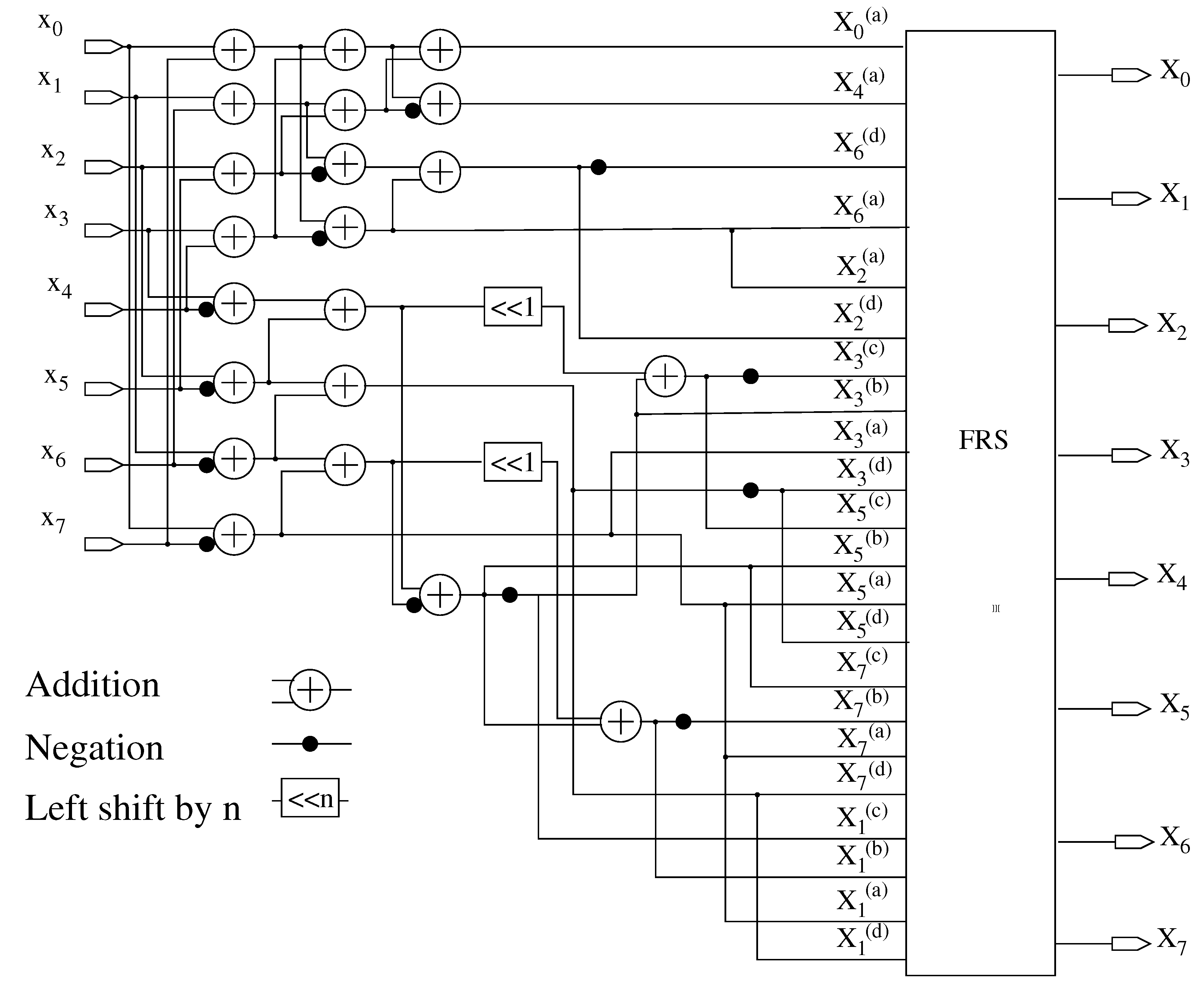
4. Final Reconstruction Step (FRS)

The final stage of the 1-D AI encoding based DCT architecture is the FRS which is used for converting the computed DCT coefficients from the infinite precision AI encoding into fixed-point representation. From [1], such conversions require the multiplication of each AI encoded output value with the finite precision approximation corresponding to each AI basis. Consider the set of 2-D AIs used in [1]. As shown in Figure 2, FRS receives at most four inputs pertaining to a single coefficient X m , each corresponding to the channels associated with AI basis values 1, z 1 , z 2 , and z 1 z 2 . Let X m ( a ) , X m ( b ) , X m ( c ) , X m ( d ) be the four encoded integers pertaining to the AI basis values 1, z 1 , z 2 , and z 1 z 2 , respectively, for a given coefficient X m . Thus X m is given by
X m = X m ( a ) · 1 + X m ( b ) · z 1 + X m ( c ) · z 2 + X m ( d ) · z 1 z 2
Here, the AI basis values z 1 , z 2 and z 1 z 2 are by definition irrational quantities. Approximating them using standard Booth Encoding [1] or Dempster–McCloud constant coefficient multipliers [18] lead to hardware intensive and highly complex FRS architectures. In this paper, we propose a novel scheme for realization of a low complexity high-accuracy FRS using number theoretical approximations based on expansion factors [19].
The main new idea here is to employ an expansion factor that could simultaneously scale the quantities z 1 , z 2 , and z 1 z 2 into integer values. That is, expansion factor α * leads to ( z 1 α * , z 2 α * , z 1 z 2 α * ) being very close to a 3-tuple of small integers. This would facilitate the usage of integer arithmetic in place of fixed-point. Such approach has been often employed by integer transform designers [19,20]. Let the quantities z 1 , z 2 , and z 1 z 2 form a vector ζ = z 1 z 2 z 1 z 2 T . An expansion factor [3] is the real number α * > 1 that satisfies the following minimization problem:
α * = arg min α > 1 α · ζ round ( α · ζ )
where · is a given error measure and round ( · ) is the rounding function. Here Euclidean norm is taken as the error measure. In the range α [ 1 , 256 ] with a precision of 10 4 , we could find the optimal value for α through computational search. Two such solutions found are α = 4.5958 and α = 167.2309 . Both these values comply with an error norm of 10 2 . Scaling of AI base z using these values can be denoted as,
α · z 1 z 2 z 1 z 2 = 12.01031370924931 4.97483482672658 12.99986988195626 12 5 13
α · z 1 z 2 z 1 z 2 = 436.995521744185 181.009471802748 473.00054429861 437 181 473
Using the above properties exhibited by the selected expansion factors, Equation (5) can be written in the following manner:
X k = 1 α α · X m ( a ) + m 1 · X m ( b ) + m 2 · X m ( c ) + m 3 · X m ( d )
where m 1 , m 2 , and m 3 are the integer constants implied by the expansion factor α such that,
{ m 1 , m 2 , m 3 } = { round ( α · z 1 ) , round ( α · z 2 ) , round ( α · z 1 z 2 ) }
For the values of α found above, these constants are { 12 , 5 , 13 } , for α = α , and { 437 , 181 , 473 } , for α = α . Here, the global multiplication by 1 / α can be easily embedded into subsequent signal processing stages. In a typical application this is absorbed by the quantizer. This approach is similar to what has been employed in several other DCT architectures [20,21,22]. Multiplication by α is a single step that is implemented as a constant multiplication. An efficient implementation of this multiplier is described next.

5. Proposed 1-D DCT Architecture

The overall architecture of the proposed 1-D DCT circuit consists of three main sub-sections: (i) a decimation block; (ii) the AI encoding based 8-point Arai DCT circuit; and (iii) the FRS. The complete system block diagram is shown in Figure 3.

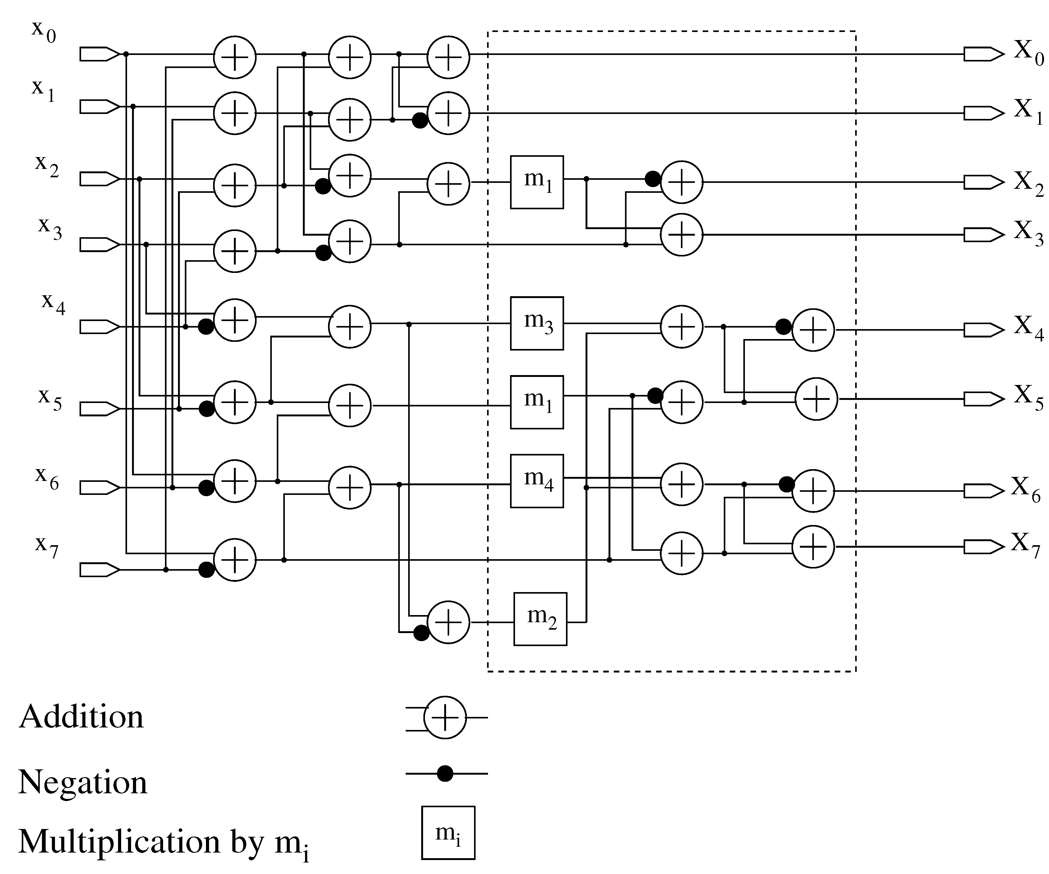
5.1. Decimation Block and 8-Point Arai-DCT Circuit

The input data stream is expected to be raster scanned with a streaming rate of F s . The decimation block converts the input sequence into 8-point columns via delay and downsample-by-8 operations. The 8 parallel channels generated pertaining to each point in the 8-point block operate at the rate F clock = F s / 8 . These 8 channels drive the 8 inputs of the 8-point Arai DCT circuit.
The 8 output channels from the decimation block drives the 8 inputs of the 8-point Arai DCT circuit. This block is a direct implementation of the signal flow graph of Figure 2. Therefore the computed result is AI encoded, resulting in a maximum of four parallel integer channels for each coefficient. As shown in Figure 3, 22 output channels are required to represent the 8-point 1-D DCT coefficients. These outputs are denoted X i ( q ) , where i = 0 , 1 , , 7 and q { a , b , c , d } representing the 4 channels 1, z 1 , z 2 , and z 1 z 2 , respectively.

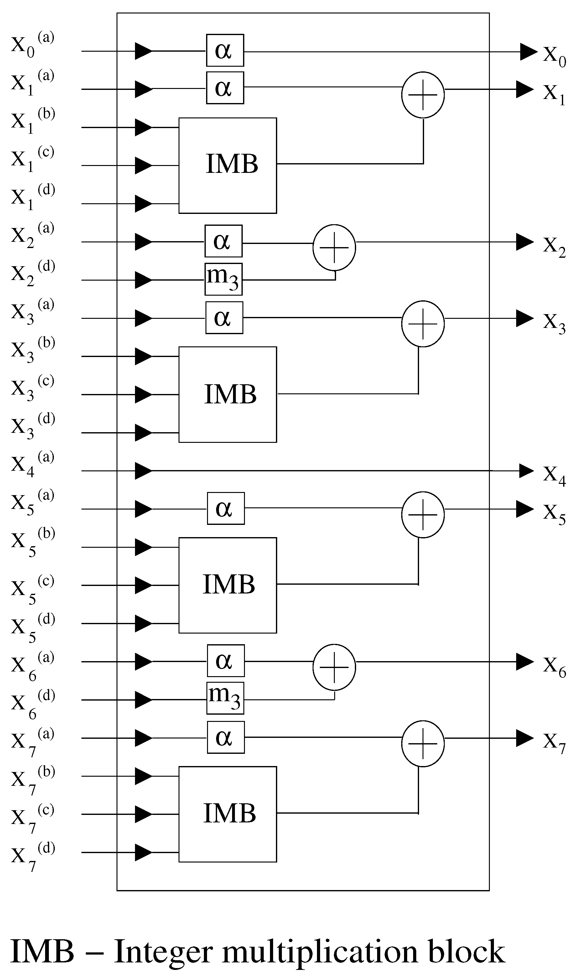
5.2. Low-Complexity Expansion-Factor FRS

The FRS is structured using the principle presented in Section 4. A block diagram of the circuit is given in Figure 4.

5.2.1. Integer Multiplication Block (IMB)

Because constants m 1 , m 2 , and m 3 in Equation (9) are integers, the associated constant coefficient multiplications can be efficiently implemented in digital VLSI hardware. Using common sub-expression elimination (CSE), these multiplications are reduced to only additions and shift operations, requiring minimal amount of hardware resources. For the set 437, 181, 473, CSE yields the following representation which requires only eight additions:
437 · X k ( b ) + 181 · X k ( c ) + 473 · X k ( d ) = 473 · X k ( b ) + X k ( c ) + X k ( d ) 36 · X k ( b ) + X k ( c ) 256 · X k ( c )
Analogously, for the set { 12 , 5 , 13 } , CSE yields the following representation which requires only five additions as shown below:
12 · X k ( b ) + 5 · X k ( c ) + 13 · X k ( d ) = 8 · X k ( b ) + X k ( d ) + 4 · X k ( b ) + X k ( c ) + X k ( d ) + X k ( d ) + X k ( c )
The above algorithms are realized using the proposed integer multiplication block (IMB) given in Figure 4.

5.2.2. Multiplication by α

A Booth encoding scheme is used to efficiently implement this constant integer multiplications using shifts and additions. Table 2 gives the Booth encoded representation for the two values of α corresponding to the two circuits described above.

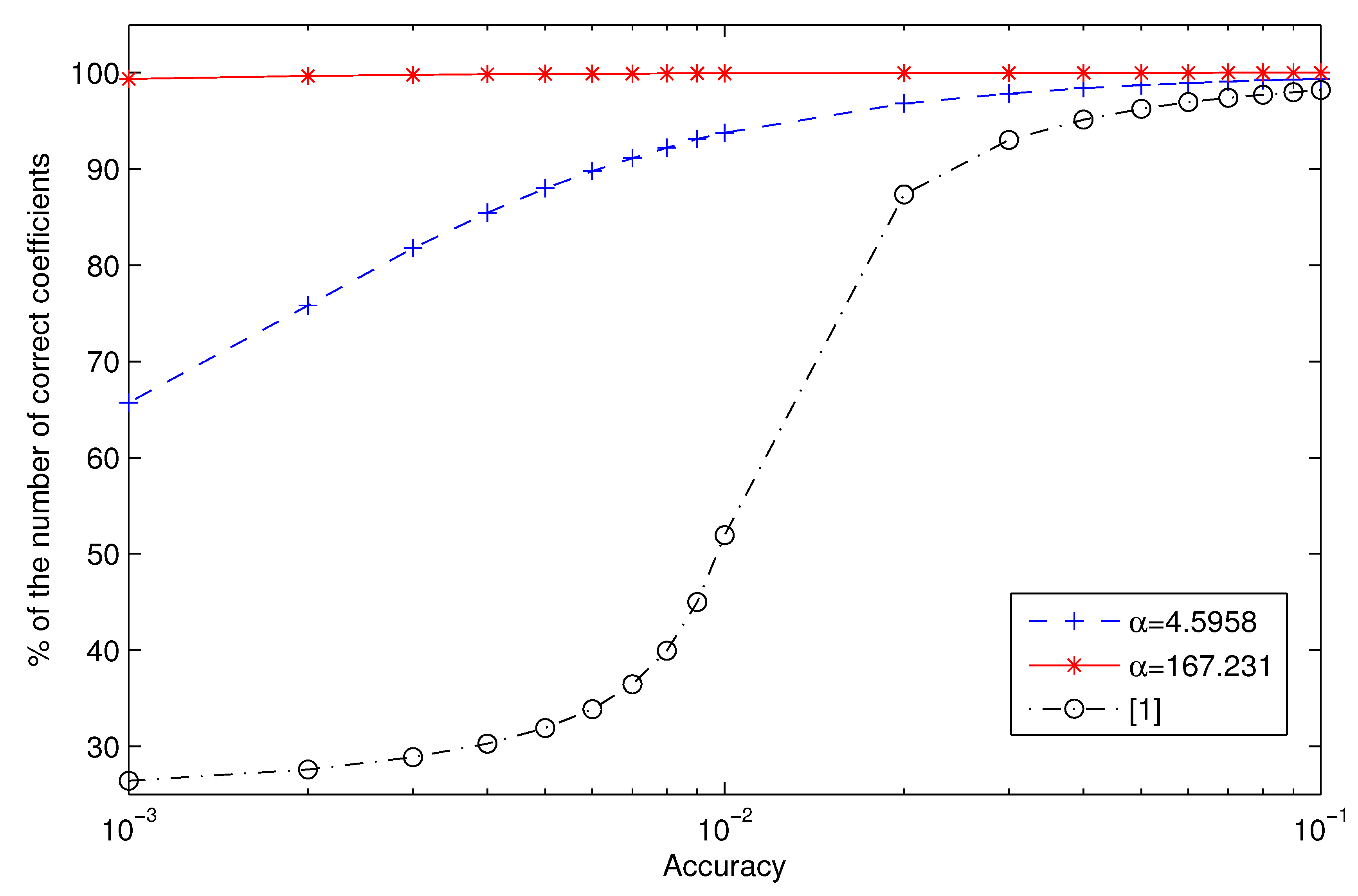
6. On-Chip Verification Using Success Rates

The proposed architecture for the expansion factor values of α = 4.5958 and α = 167.2309 , as well as the design proposed in [1], were physically implemented and tested on-chip using field programmable gate array (FPGA) technology. We used a Xilinx ML605 development kit which is populated with a 40 nm CMOS Xilinx Virtex-6 XC6VLX240T FPGA device. The JTAG interface was used to input the test vectors to the device from the Matlab workspace. Then the measured outputs from the FPGA were returned to the Matlab workspace via the same interface. Hardware computed coefficients were compared to the ideal numerical values evaluated at nearly machine precision (64-bits) on Matlab. The machine precision is high-enough for typical video and imaging applications to be considered close to infinite precision. First the experiment was conducted by sending test vectors of length 8 × 10 6 , 8- and 12-bit randomly generated values through 8- and 12-bit versions of the designs. The success-rate obtained as the percentage of coefficients having an error ratio less than a threshold value is plotted for varying thresholds on a log scale in Figure 5 and Figure 6 for signal input bit size W = 8 and W = 12 respectively. The AI component of the algorithm (that is, up to the FRS) is completely error-free. The test was also conducted on 512 × 512 pixel versions of standard test images Lena, Cameraman, and Livingroom, and the success rates are tabulated in Table 3.
The results show that the design corresponding to the expansion factor α = 167.2309 exhibit a far superior accuracy than the other two designs. We found that 99 % of coefficients could fulfill an error ceiling of 0.1% whereas the corresponding values for α = 4.5958 design and the design proposed in [1] are 65 % and 25 % , respectively. Comparing the latter two designs it can be seen that the α = 4.5958 expansion factor design shows much better accuracy compared with the design in [1].

7. Results

All three designs were implemented both in 65 nm CMOS process from TSMC up to synthesis level for application-specific integrated circuit (ASICs) and physically implemented using 40 nm CMOS Xilinx Virtex-6 XC6VLX240T FPGA for obtaining area ( A ) , critical path delay ( T ) and power consumption ( P D ) for comparison. The respective results are shown in Table 4 and Table 5 for our FPGA-based physical implementation and ASIC synthesis, respectively. The accuracy results in Figure 5 and Figure 6 are from measurements from the hardware physical implementations of the FPGA realizations as obtained from the Xilinx ML605 prototyping board.

7.1. 40 nm CMOS Virtex-6 FPGAs

The designs were implemented for an input size of 8 bits in Xilinx Virtex-6 XC6VLX240T FPGA using Xilinx ISE tools. The resulting area, critical path delay (inversely proportional to the maximum clock speed) and power consumptions are given in Table 4.

7.2. Area Utilization

FPGA resources are given in Table 4 in terms of slices, slice registers, and slice look-up-tables (LUTs). It is observed that both the designs using proposed expansion factor based FRS consume less resources than the current state-of-the-art in comparable designs in the literature [1]. Furthermore, the proposed expansion factor based designs provide significantly better accuracy at a much lower hardware cost. The design using α = 4.5958 expansion factor consumes the least FPGA resources although it exhibits less accuracy compared with the design using α = 167.2309 as the choice of expansion factor. The proposed designs for α = 4.5958 and α = 167.2309 show 43% and 14% reductions in area, respectively, compared to our reference design [1] when realized in Virtex-6 FPGA technology.

7.3. Operating Frequency

A similar pattern to the area consumption is seen with the design using α = 4.5958 expansion factor running at the highest frequency followed by α = 167.2309 expansion factor and the design proposed in [1] in respective order. The difference in the size of the designs as discussed under area utilization can be assumed to be the dominant factor in determining the critical path, resulting in the observed behaviour. The proposed designs for α = 4.5958 and α = 167.2309 show 48% and 27% reductions in area-time complexity metric ( A T ) , respectively, compared to the reference design [1] when realized in Virtex-6 FPGA technology.

7.4. Power Consumption

The dynamic power consumption of a FPGA design consists of components form clocks, logic and signals. A breakdown of these components for all three designs along with the total dynamic power consumption is given in Table 4. The proposed designs for α = 4.5958 and α = 167.2309 show 29% and 20% reductions in dynamic power consumption, respectively, compared to the reference design [1] when realized in 40 nm CMOS Xilinx Virtex-6 FPGA technology.

7.5. 65 nm CMOS for ASICs

The designs were implemented for an input size of 8 bits in 65 nm CMOS general purpose standard cells from TSMC at an operating voltage of 900 mV. The resulting VLSI area, critical path delay T cpd which is inversely proportional to the maximum clock speed such that F clock = 1 / T cpd and dynamic power P D , leakage power P L , as well as the total power consumption P T are given in Table 5.

7.6. Area Utilization

ASIC resources are given in Table 5 in terms of area in μ m 2 . It is observed that both designs using proposed expansion factor based FRS consume less resources than the current state-of-art in comparable designs in the literature [1]. The design using α = 4.5958 expansion factor consumes the least ASIC resources. The proposed designs for α = 4.5958 and α = 167.2309 show 11% and 3% reductions in area, respectively, compared to our reference design [1] when realized in 65 nm CMOS general purpose standard cells from TSMC.

7.7. Operating Frequency

The proposed designs for α = 4.5958 and α = 167.2309 show 11% and 3% reductions in area-time complexity metric, respectively, compared to the reference design [1]. All three designs were synthesized for a T cpd 0.48 ns clock period corresponding to a maximum speed of F clock = F s / 8 = 2.083 GHz . Because this clock frequency is for the slowest inner core of the architecture, the architecture potentially supports high-performance video processing having input word rates (pixels per second) at F s = 16.664 GHz, which in turn implies a serial data processing rate of 133.312 Gbps for an 8-bit system. In practice, it is unlikely that popular image sensors would be able to deliver such high levels of pixel read-out data unless used in a specialized scientific instrument. The synthesis results indicate potential suitability for 100 Gbps Ethernet video feeds. However, it is reasonable to assume that the core would in practice be clocked at much lower rates than 2.083 GHz, which would proportionately reduce the dynamic power consumption since P D F clock . Hence, power estimates assume 100 MHz clock, which implies a pixel rate of 800 MPixels/seconds, and a serial data rate for the system at 6.4 Gbps (for W = 8 bit precision) and 9.6 Gbps (for W = 12 bit precision), which is well within the range of current high-performance digital video processing systems. As an aside, we note that 9.6 Gbps serial-deserializers (SERDES) are available as hard silicon in many FPGA systems.

7.8. Power Consumption

All 65 nm designs assume a 900 mV supply at a clock frequency of F clock = 100 MHz for all three designs. The dynamic power consumption of an ASIC design consists of components form clocks, logic and signals. A breakdown of these components for all three designs is given in Table 5. The proposed designs for α = 4.5958 and α = 167.2309 show 8% and 1.5% reductions in dynamic power consumption, respectively, compared to the reference design [1]. The total power consumption was 9% and 1.5% down compared to the reference. Although the 65 nm CMOS design for α = 167.2309 shows only a marginal reduction in area and power consumption compared to [1] realized on the same technology, it should be noted that the proposed design has a significant improvement in computational accuracy. At the highest precision level of 0.1% , there is approximately a 300 % increase in the number of computed coefficients for α = 167.2309 compared to [1]. For α = 4.5958 , the improvement in accuracy is still significant at better than 150 % for the most accurate coefficients at 0.1% .
Because both circuits show accuracy of over 90% for a tolerance level of 1%, it might be possible to reduce the power supply voltage with a penalty in arithmetic errors leading to lower power at lower accuracy.

7.9. Overall Comparison With Existing Architectures

CMOS implementations of DCT architectures that are comparable to the proposed architecture are tabulated in Table 6 with a detailed comparison between their salient features and reported results. Results obtained from CMOS implementation using 8-bit input size for the proposed architectures for α = 4.5958 and α = 167.2309 along with the implementation for [1] was used in this comparison.

8. Conclusions

In this paper, we proposed a low complexity digital VLSI architecture for the computation of an algebraic integer (AI) based 8-point Arai-DCT. AI encoding is used on the Arai fast algorithm for DCT computation, and a novel FRS structure based on expansion factors is employed. By the use of CSE and Booth encoding the optimum circuits are synthesized for two different FRS structures corresponding to two suitable expansion factors. The designs are implemented in both 65 nm CMOS general purpose standard cells from TSMC and 40 nm CMOS Xilinx Virtex-6 XC6VLX240T FPGA technology.
The results show an improvement of 43 % in area and 29 % in power consumption for our FPGA implementation and 10 % in area and 8 % in power consumption for our CMOS standard cell implementation when α = 4.5958 is used. The expansion factor of α = 167.2309 yields an improvement of 300 % in the number of DCT coefficients having error ≤ 0.1% , with improvements of 13 % and 19 % in area and power consumption for the FPGA implementation and corresponding improvements of 2.5% and 1.5% for the ASIC implementation. We therefore conclude that the α = 4.5958 design is suitable in cases where lowest power, lowest area, and good accuracy is required, and the second expansion factor α = 167.2309 is suitable when accuracy is the most important requirement of the application. An example of such an application may be high-definition high-dynamic range imaging. Both proposed architectures excel as per metrics considered (area, power, area-time, throughput, accuracy) when compared to the reference design [1] for both 65 nm CMOS standard cells and 40 nm Virtex-6 FPGA technology.

Acknowledgements

The authors are grateful for support from the University of Akron College of Engineering; NSERC (Canada); CNPq and FACEPE (Brazil); University of Waterloo; and the Canadian Microelectronics Corporation (CMC).

References

  1. Dimitrov, V.; Wahid, K.; Jullien, G. Multiplication-free 8 × 8 2D DCT architecture using algebraic integer encoding. Electron. Lett. 2004, 40, 1310–1311. [Google Scholar] [CrossRef]
  2. Blinn, J. What’s that deal with the DCT? IEEE Comput. Graph. Appl. 1993, 13, 78–83. [Google Scholar] [CrossRef]
  3. Britanak, V.; Yip, P.; Rao, K.R. Discrete Cosine and Sine Transforms; Academic Press: Waltham, MA, USA, 2007; p. 274. [Google Scholar]
  4. Cintra, R.J. An integer approximation method for discrete sinusoidal transforms. J. Circuits Syst. Signal Process. 2011, 30, 1481–1501. [Google Scholar] [CrossRef]
  5. Tun, I.D.; Lee, S.U. On the fixed-point-error analysis of several fast DCT algorithms. IEEE Trans. Circuits Syst. Video Technol. 1993, 3, 27–41. [Google Scholar]
  6. Lee, B. A new algorithm to compute the discrete cosine transform. IEEE Trans. Acoust. Speech Signal Process. 1984, 32, 1243–1245. [Google Scholar]
  7. Hou, H. A fast recursive algorithm for computing the discrete cosine transform. IEEE Trans. Acoust. Speech Signal Process. 1987, 35, 1455–1461. [Google Scholar]
  8. Vitterli, M. Simple FFT and DCT algorithms with reduced number of operations. Signal Process. 1984, 6, 267–278. [Google Scholar] [CrossRef]
  9. Duhamel, P.; H’Mida, H. New 2nDCT Algorithms Suitable for VLSI Implementation. In >Proceedings of the IEEE International Conference on Acoustics, Speech, and Signal Processing (ICASSP ’87), Boston, MA, USA, 14–16 April 1987; Volume 12, pp. 1805–1808. [Google Scholar]
  10. Loeffler, C.; Ligtenberg, A.; Moschytz, G. Practical Fast 1-D DCT Algorithms with 11 Multiplications. In Proceedings of the 1989 International Conference on Acoustics, Speech, and Signal Processing (ICASSP ’89), Glasgow, Scotland, 23–26 May 1989; Volume 2, pp. 988–991. [Google Scholar]
  11. Arai, Y.; Agui, T.; Nakajima, M. A fast DCT-SQ scheme for images. Trans. IEICE 1988, e 71, 1095–1097. [Google Scholar]
  12. Tseng, B.; Miller, W. On computing the discrete cosine transform. IEEE Trans. Comput. 1978, C-27, 966–968. [Google Scholar] [CrossRef]
  13. Dimitrov, V.; Jullien, G.; Miller, W. A New DCT Algorithm Based on Encoding Algebraic Integers. In Proceedings of the IEEE International Conference on Acoustics, Speech and Signal Processing, Seattle, WA, USA, 12–15 May 1998; Volume 3, pp. 1377–1380. [Google Scholar]
  14. Baghaie, R.; Dimitrov, V. Systolic implementation of real-valued discrete transforms via algebraic integer quantization. Comput. Math. Appl. 2001, 41, 1403–1416. [Google Scholar] [CrossRef]
  15. Dimitrov, V.; Jullien, G. Multidimensional algebraic-integer encoding for high performance implementation of DCT and IDCT. Electron. Lett. 2003, 39, 602–603. [Google Scholar] [CrossRef]
  16. Fu, M.; Jullien, G.; Dimitrov, V.; Ahmadi, M.; Miller, W. The Application of 2D Algebraic Integer Encoding to a DCT IP Core. In Proceedings of the 3rd IEEE International Workshop on System-on-Chip for Real-Time Applications, Calgary, Canada, 30 June–2 July 2003; pp. 66–69. [Google Scholar]
  17. Fu, M.; Jullien, G.; Dimitrov, V.; Ahmadi, M. A Low-Power DCT IP Core Based on 2D Algebraic Integer Encoding. In Proceedings of the 2004 International Symposium onCircuits and Systems (ISCAS ’04), Vancouver, Canada, 23–26 May 2004; Volume 2, pp. 765–768. [Google Scholar]
  18. Madanayake, H.L.P.A.; Cintra, R.J.; Onen, D.; Dimitrov, V.S.; Bruton, L.T. Algebraic Integer Based 8 × 8 2-D DCT Architecture for Digital Video Processing. In Proceedings of the 2011 IEEE International Symposium on Circuits and Systems (ISCAS ’11), Rio de Janeiro, Brazil, 15–18 May 2011; pp. 1247–1250. [Google Scholar]
  19. Plonka, G. A global method for invertible integer DCT and integer wavelet algorithms. Appl. Comput. Harmon. Anal. 2004, 16, 79–110. [Google Scholar] [CrossRef]
  20. Cintra, R.J.; Bayer, F.M. A DCT approximation for image compression. IEEE Signal Process. Lett. 2011, 18, 579–583. [Google Scholar] [CrossRef]
  21. Bouguezel, S.; Ahmad, M.O.; Swamy, M.N.S. Low-complexity 8 × 8 transform for image compression. Electron. Lett. 2008, 44, 1249–1250. [Google Scholar] [CrossRef]
  22. Bouguezel, S.; Ahmad, M.O.; Swamy, M.N.S. A Low-Complexity Parametric Transform for Image Compression. In Proceedings of the 2011 IEEE International Symposium on Circuits and Systems, Rio de Janeiro, Brazil, 15–18 May 2011. [Google Scholar]
  23. Gong, D.; He, Y.; Cao, Z. New cost-effective VLSI implementation of a 2-D discrete cosine transform and its inverse. IEEE Trans. Circuits Syst. Video Technol. 2004, 14, 405–415. [Google Scholar] [CrossRef]
  24. Shams, A.; Bayoumi, M. A 108 Gbps, 1.5 GHz 1D-DCT Architecture. In Proceedings of the IEEE International Conference on Application-Specific Systems, Architectures, and Processors, Boston, MA, USA, 10–12 July 2000; pp. 163–172. [Google Scholar]
  25. Ghosh, S.; Venigalla, S.; Bayoumi, M. Design and Implementaion of a 2D-DCT Architecture Using Coefficient Distributed Arithmetic [Implementaion Read Implementation]. In Proceedings of the IEEE Computer Society Annual Symposium on VLSI, Tampa, FL, USA, 11–12 May 2005; pp. 162–166. [Google Scholar]
Figure 1. Block diagram of an 8-point Arai 1-D DCT architecture [13].
Jlpea 02 00127 g001
Figure 2. Block diagram of the AI encoding based 1-D DCT architecture [1].
Jlpea 02 00127 g002
Figure 3. Block diagram of the proposed AI encoding based 1-D DCT architecture showing multirate input Section [18], Arai AI-block and expansion-factor FRS.
Jlpea 02 00127 g003
Figure 4. Block diagram of the proposed FRS block.
Jlpea 02 00127 g004
Figure 5. Accuracy results for W = 8 .
Jlpea 02 00127 g005
Figure 6. Accuracy results for W = 12 .
Jlpea 02 00127 g006
Table 1. 2-D error free multiplier encoding.
m 1 0 0 0 1 m 3 0 0 2 0
m 2 0 1 1 0 m 4 0 2 0 0
Table 2. Booth encoding of the expansion factors α .
α Representation
4.5961 2 2 + 2 1 + 2 4 + 2 5 + 2 9
167.2309 2 7 + 2 5 + 2 3 2 0 + 2 2 2 6 2 8
Table 3. Success rates of DCT coefficient computation for standard test images.
Percentage tolerance
DesignLenaCameramanLivingroom
10%1%0.01%10%1%0.01%10%1%0.01%
α = 4.595899.4393.8650.6599.4494.0752.4899.3793.8650.81
α = 167.23199.9999.9493.4499.9999.9693.5399.9999.9393.41
[1]98.4452.3326.1098.7254.5226.4998.3952.8126.44
Table 4. Area-speed and power consumption for FPGA implementation.
DesignAreaSpeedATPower (mW)
LUTsRegistersSlices(MHz)Slices · μ sClocksLogicSignalsTotal
α = 4.59581,412602409268.71.52213121136
α = 167.2312,217696621288.12.15510171441
[1]2,656702721244.42.94910221951
Table 5. Area-speed and power consumption for CMOS 65 nm ASIC implementation.
DesignAreaSpeedATPower (mW)
( μ m 2 )(MHz)( μ m 2 · μ s)DynamicLeakageTotal
α = 4.595848,386.882,083.3323.234.360.3654.725
α = 167.23152,904.882,083.3325.4  4.670.4245.094
[1]54,299.522,083.3326.064.740.4275.167
Table 6. Comparison of the proposed implementation with published 1-D DCT implementations.
ParameterGong et al. [23]Shams et al. [24]Ghosh et al. [25]Dimitrov et al. [1]Proposed architectures
α = 4.5958 α = 167.231
Measured resultsNoNoNoYesYesYes
Structure Vector matrix DCT coreCoefficient arithmetic DCT core based DCTCoefficient arithmetic DCT core based DCTAI based DCT+ Booth encoded FRSAI based DCT+ expansion factor FRS
Multipliers800000
Operating frequency 125 MHz 1.5 GHz 50 MHz 2.08 GHz 2.08 GHz 2.08 GHz
Pixel rate125 Mpix/s108 Gb/s10.922 Mpix/s16.67 Gb/s16.67 Gb/s16.67 Gb/s
Power consumptionN/A210 mW12.45 mW5.167 mW4.725 mW5.094 mW
Technology 0.25  μ m CMOS0.35  μ m CMOS0.12  μ m CMOS   65 nm CMOS   65 nm CMOS   65 nm CMOS
Independently adjustable precision No No No Yes Yes Yes
Publisher’s Note: MDPI stays neutral with regard to jurisdictional claims in published maps and institutional affiliations.

