A Minimum Leakage Quasi-Static RAM Bitcell

Abstract
:1. Introduction
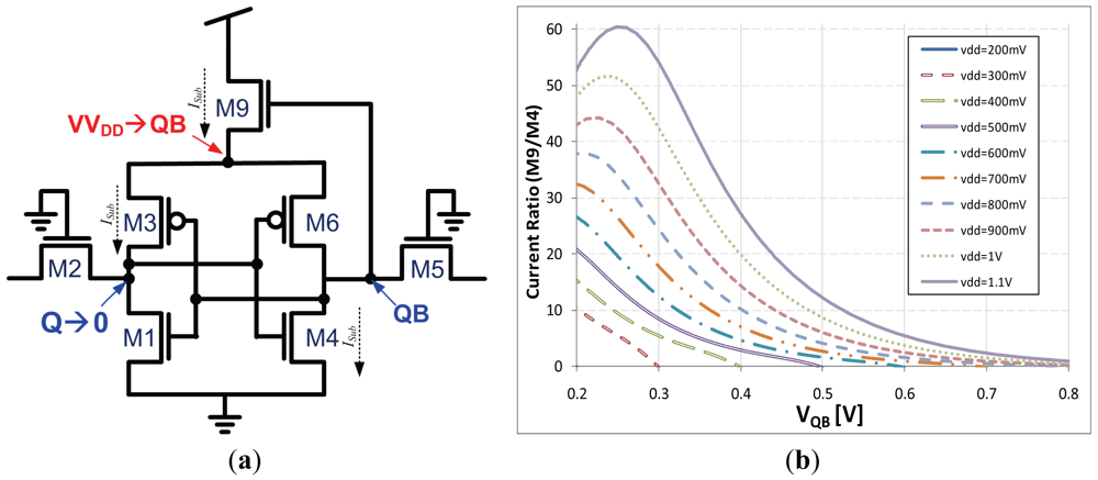
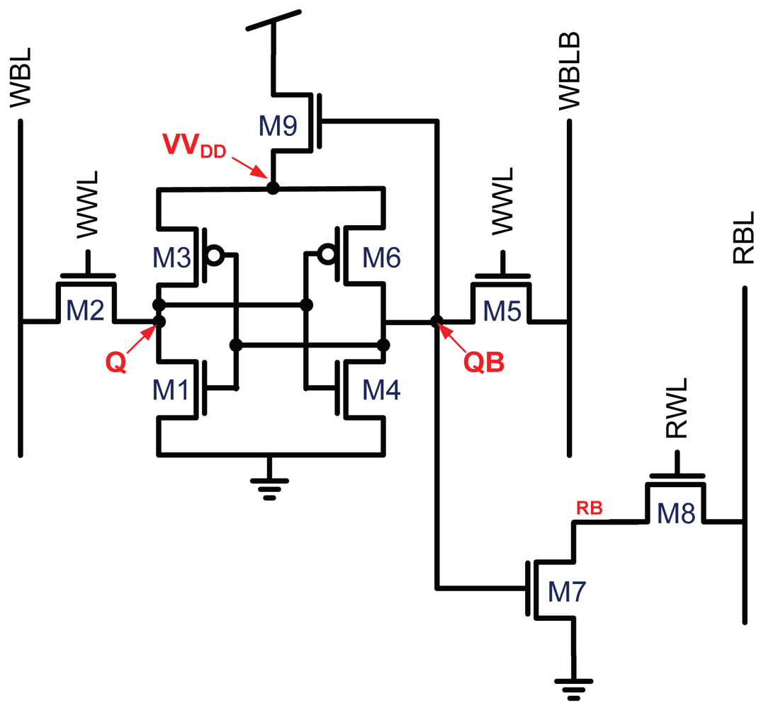
2. The Proposed 9T Bitcell Design
2.1. Description
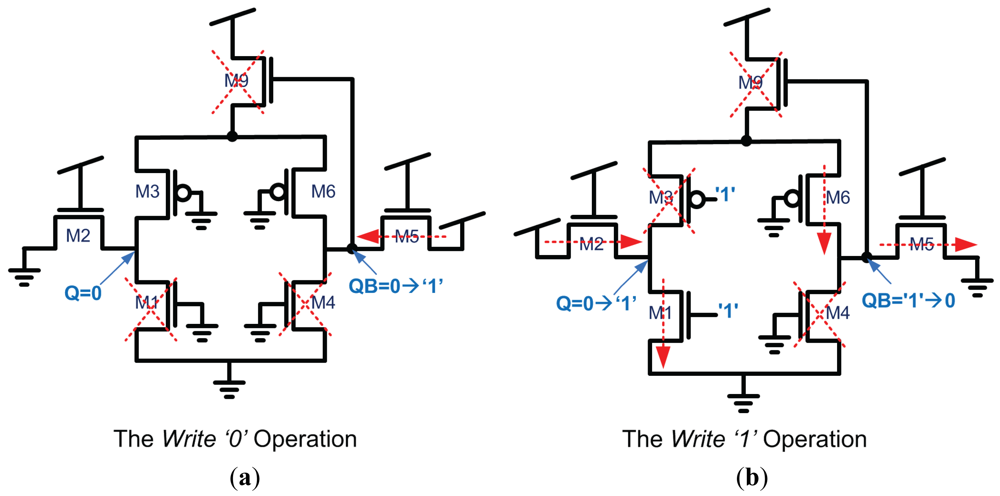
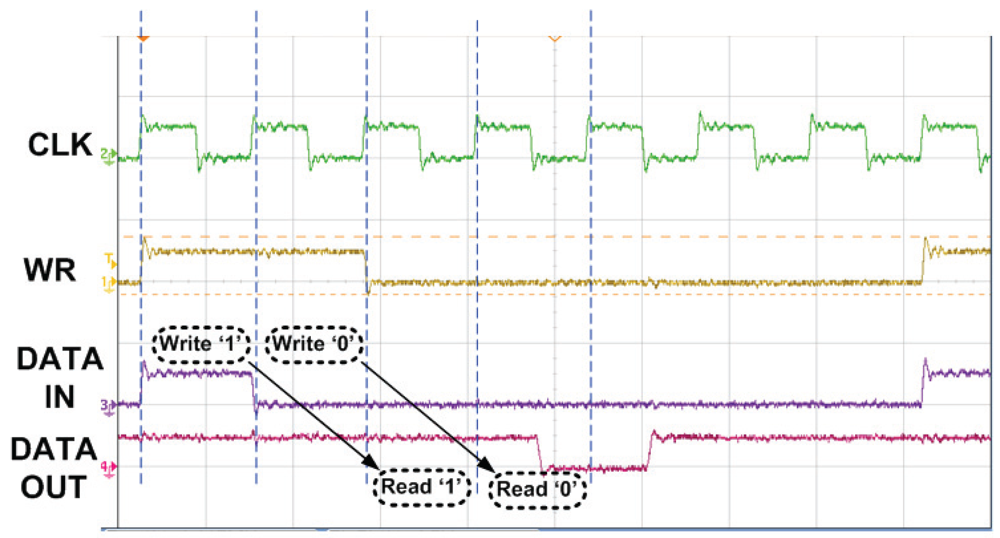
2.2. Write Operation
2.3. Read Operation
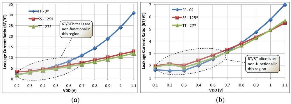
3. Cell Stability
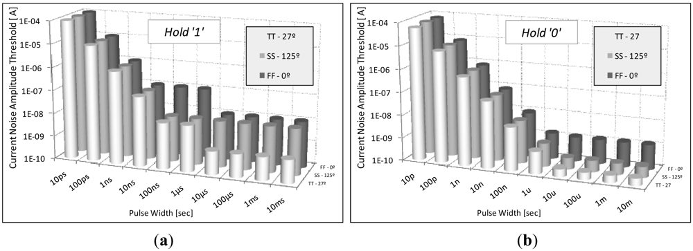
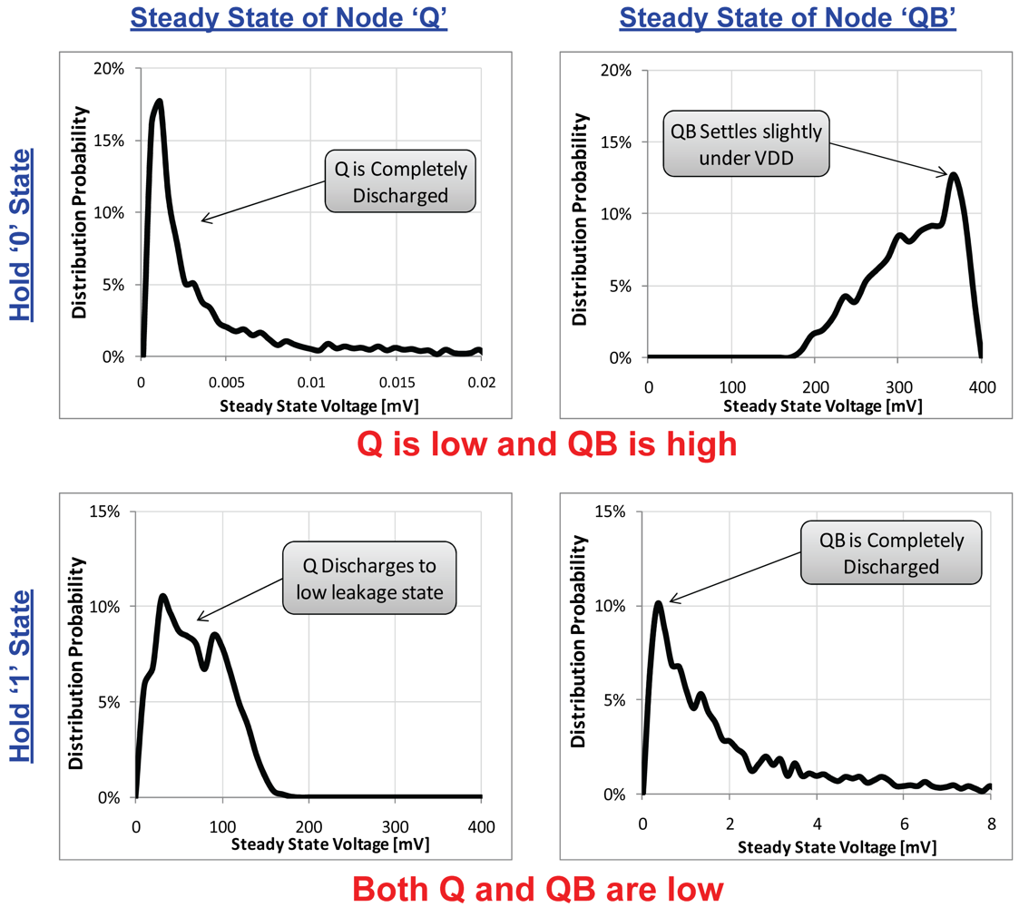
3.1. Hold Stability
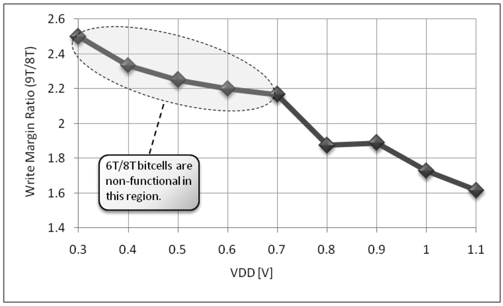
3.2. Read and Write Stability
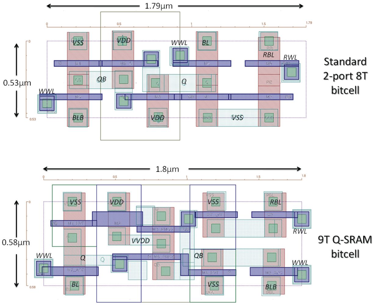
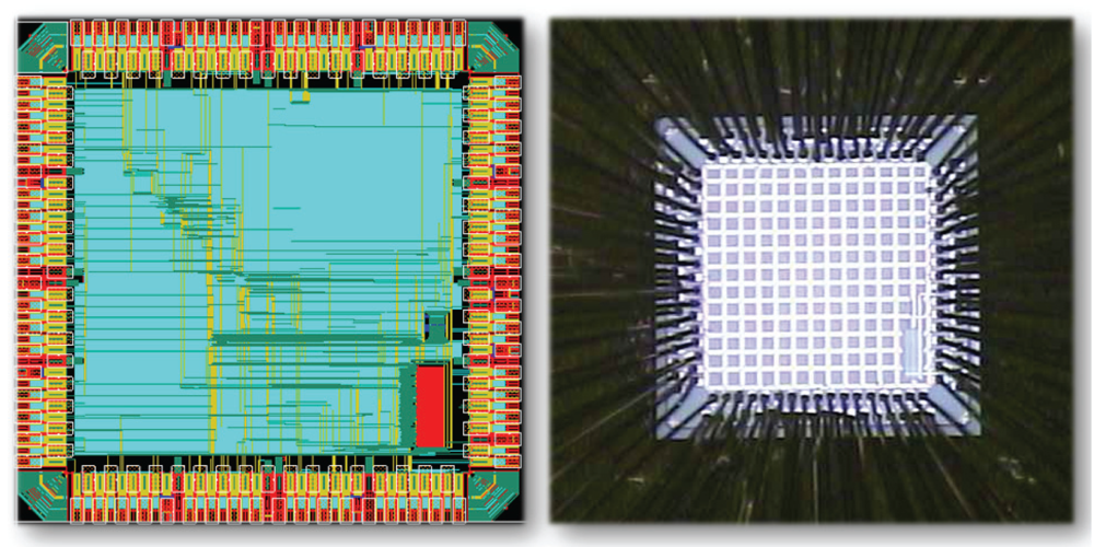
4. Implementation and Performance
5. Conclusions


| Process Technology | TSMC 40 nm LP | |
| Simulator | Cadence spectre | |
| # of Transistors | 9 | |
| Minimum VDD | 300mV | |
| Comparison with standard 8T bitcell | Hold ‘1’ State | Hold ‘0’ State |
| Static Power Reduction @700 mV | 7.9× | 3.5× |
| Static Power Reduction @1.1 V | 12× | 5.7× |
| Read Access Ratio @700 mV | 1× | 1.74× |
| Write Margin Ratio @700 mV | 2.2× | |
| Write Access Ratio @700 mV | 0.17× | |
Acknowledgments
References
- Kim, N.S.; Flautner, K.; Blaauw, D.; Mudge, T. Circuit and Microarchitectural Techniques for Reducing Cache Leakage Power. IEEE Trans. Very Large Scale Integr. Syst. 2004, 12, 167–184. [Google Scholar]
- Calhoun, B.H.; Chandrakasan, A.P. A 256-Kb 65-nm Sub-Threshold SRAM Design for Ultra-Low-Voltage Operation. IEEE J. Solid State Circuits 2007, 42, 680–688. [Google Scholar]
- Yang, B.D.; Kim, L.S. A Low-Power SRAM using Hierarchical Bit Line and Local Sense Amplifiers. IEEE J. Solid State Circuits 2005, 40, 1366–1376. [Google Scholar]
- Wang, C.C.; Lee, C.L.; Lin, W.J. A 4-Kb Low-Power SRAM Design with Negative Word-Line Scheme. IEEE Trans. Circuits Syst. I: Regul. Papers 2007, 54, 1069–1076. [Google Scholar]
- Razavipour, G.; Afzali-Kusha, A.; Pedram, M. Design and Analysis of Two Low-Power SRAM Cell Structures. IEEE Trans. Very Large Scale Integr. Syst. 2009, 17, 1551–1555. [Google Scholar]
- Liu, Z.; Kursun, V. Characterization of a Novel Nine-Transistor SRAM Cell. IEEE Trans. Very Large Scale Integr. Syst. 2008, 16, 488–492. [Google Scholar]
- Levacq, D.; Dessard, V.; Flandre, D. Low Leakage SOI CMOS Static Memory Cell with Ultra-Low Power Diode. IEEE J. Solid State Circuits 2007, 42, 689–702. [Google Scholar]
- Chandrakasan, A.P.; Daly, D.C.; Finchelstein, D.F.; Kwong, J.; Ramadass, Y.K.; Sinangil, M.E.; Sze, V.; Verma, N. Technologies for Ultradynamic Voltage Scaling. Proc. IEEE 2010, 98, 191–214. [Google Scholar]
- Verma, N.; Chandrakasan, A.P. A 256 Kb 65 Nm 8T Subthreshold SRAM Employing Sense-Amplifier Redundancy. IEEE J. Solid State Circuits 2008, 43, 141–149. [Google Scholar]
- Kim, T.H.; Liu, J.; Kim, C.H. An 8T Subthreshold SRAM Cell Utilizing Reverse Short Channel Effect for Write Margin and Read Performance Improvement. Proceedings of the IEEE Custom Integrated Circuits Conference (CICC '07), San Jose, CA, USA, 16–19 September 2007; pp. 241–244.
- Chang, I.J.; Kim, J.J.; Park, S.P.; Roy, K. A 32 Kb 10T Sub-Threshold SRAM Array with Bit-Interleaving and Differential Read Scheme in 90 Nm CMOS. IEEE J. Solid State Circuits 2009, 44, 650–658. [Google Scholar]
- Wang, A.; Calhoun, B.H.; Chandrakasan, A.P. Sub-Threshold Design for Ultra Low-Power Systems; Springer Verlag: Secaucus, NJ, USA, 2006. [Google Scholar]
- Wang, J.; Nalam, S.; Calhoun, B.H. Analyzing Static and Dynamic Write Margin for Nanometer SRAMs. Proceeding of the 13th International Symposium on Low Power Electronics and Design, Bangalore, India, 11–13 August 2008; pp. 129–134.
- Sharifkhani, M.; Sachdev, M. SRAM Cell Stability: A Dynamic Perspective. IEEE J. Solid State Circuits 2009, 44, 609–619. [Google Scholar]
- Frustaci, F.; Corsonello, P.; Perri, S.; Cocorullo, G. Techniques for Leakage Energy Reduction in Deep Submicrometer Cache Memories. IEEE Trans. Very Large Scale Integr. Syst. 2006, 14, 1238–1249. [Google Scholar]
- Seevinck, E.; List, F.J.; Lohstroh, J. Static-Noise Margin Analysis of MOS SRAM Cells. IEEE J. Solid State Circuits 1987, 22, 748–754. [Google Scholar]
- Lohstroh, J. Static and Dynamic Noise Margins of Logic Circuits. IEEE J. Solid State Circuits 1979, 14, 591–598. [Google Scholar]
- Ding, L.; Mazumder, P. Dynamic Noise Margin: Definitions and Model. Proceedings of the 17th International Conference on VLSI Design, Mumbai, India; 2004; pp. 1001–1006. [Google Scholar]
- Huang, G.M.; Dong, W.; Ho, Y.; Li, P. Tracing SRAM Separatrix for Dynamic Noise Margin Analysis Under Device Mismatch. Proceedings of the Behavioral Modeling and Simulation Workshop (BMAS 2007), San Jose, CA, USA, 20–21 September 2007; pp. 6–10.
- Zhang, Y.; Li, P.; Huang, G.M. Separatrices in High-Dimensional State Space: System-Theoretical Tangent Computation and Application to SRAM Dynamic Stability Analysis. Proceedings of the 47th ACM/IEEE Design Automation Conference (DAC), Anaheim, CA, USA; 2010; pp. 567–572. [Google Scholar]
- Wieckowski, M.; Sylvester, D.; Blaauw, D.; Chandra, V.; Idgunji, S.; Pietrzyk, C.; Aitken, R. A Black Box Method for Stability Analysis of Arbitrary SRAM Cell Structures. Proceedings of the Design, Automation & Test in Europe Conference & Exhibition (DATE), Dresden, Germany, 8–12 March 2010; pp. 795–800.
© 2011 by the authors; licensee MDPI, Basel, Switzerland. This article is an open access article distributed under the terms and conditions of the Creative Commons Attribution license (http://creativecommons.org/licenses/by/3.0/).
Share and Cite
Teman, A.; Pergament, L.; Cohen, O.; Fish, A. A Minimum Leakage Quasi-Static RAM Bitcell. J. Low Power Electron. Appl. 2011, 1, 204-218. https://doi.org/10.3390/jlpea1010204
Teman A, Pergament L, Cohen O, Fish A. A Minimum Leakage Quasi-Static RAM Bitcell. Journal of Low Power Electronics and Applications. 2011; 1(1):204-218. https://doi.org/10.3390/jlpea1010204
Chicago/Turabian StyleTeman, Adam, Lidor Pergament, Omer Cohen, and Alexander Fish. 2011. "A Minimum Leakage Quasi-Static RAM Bitcell" Journal of Low Power Electronics and Applications 1, no. 1: 204-218. https://doi.org/10.3390/jlpea1010204