<?xml version="1.0" encoding="UTF-8"?>
<!DOCTYPE article PUBLIC "-//NLM//DTD Journal Publishing DTD v2.3 20070202//EN" "journalpublishing.dtd">
<article xmlns:mml="http://www.w3.org/1998/Math/MathML" xmlns:xlink="http://www.w3.org/1999/xlink" xml:lang="en" article-type="research-article">
<front>
<journal-meta>
<journal-id journal-id-type="publisher-id">Journal of Low Power Electronics and Applications</journal-id>
<journal-title>Journal of Low Power Electronics and Applications</journal-title>
<issn pub-type="epub">2079-9268</issn>
<publisher>
<publisher-name>Molecular Diversity Preservation International (MDPI)</publisher-name></publisher></journal-meta>
<article-meta>
<article-id pub-id-type="doi">10.3390/jlpea1010131</article-id>
<article-id pub-id-type="publisher-id">jlpea-01-00131</article-id>
<article-categories>
<subj-group>
<subject>Article</subject></subj-group></article-categories>
<title-group>
<article-title>Path Specific Register Design to Reduce Standby Power Consumption</article-title></title-group>
<contrib-group>
<contrib contrib-type="author">
<name><surname>Salman</surname><given-names>Emre</given-names></name><xref ref-type="corresp" rid="c1-jlpea-01-00131"><sup>*</sup></xref></contrib>
<contrib contrib-type="author">
<name><surname>Qi</surname><given-names>Qi</given-names></name></contrib>
<aff id="af1-jlpea-01-00131">Department of Electrical and Computer Engineering, Stony Brook University, Stony Brook, NY 11794, USA; E-Mail: <email>qiqi@ece.sunysb.edu</email></aff></contrib-group>
<author-notes>
<corresp id="c1-jlpea-01-00131">
<label>*</label> Author to whom correspondence should be addressed; E-Mail: <email>emre@ece.sunysb.edu</email>; Tel.: +1-631-632-8419; Fax: +1-631-632-8494.</corresp></author-notes>
<pub-date pub-type="collection">
<year>2011</year></pub-date>
<pub-date pub-type="epub">
<day>15</day>
<month>04</month>
<year>2011</year></pub-date>
<volume>1</volume>
<issue>1</issue>
<fpage>131</fpage>
<lpage>149</lpage>
<history>
<date date-type="received">
<day>25</day>
<month>11</month>
<year>2010</year></date>
<date date-type="rev-recd">
<day>11</day>
<month>04</month>
<year>2011</year></date>
<date date-type="accepted">
<day>13</day>
<month>04</month>
<year>2011</year></date></history>
<permissions>
<copyright-statement>© 2011 by the authors; licensee MDPI, Basel, Switzerland.</copyright-statement>
<copyright-year>2011</copyright-year>
<license>
<p>This article is an open access article distributed under the terms and conditions of the Creative Commons Attribution license (http://creativecommons.org/licenses/by/3.0/).</p></license></permissions>
<abstract>
<p>A methodology is proposed to design low leakage registers by considering the type of timing path, <italic>i.e.</italic>, short or long, and type of register, <italic>i.e.,</italic> launching or capturing. Three different dual threshold voltage registers are developed where each register trades, depending upon the timing path, a different timing constraint for reducing the leakage current. For example, the first proposed register is used as a launching register in a noncritical path, trading clock-to-Q delay for leakage current. Other timing constraints such as setup and hold times are maintained the same not to introduce any timing violations. Alternatively, the second and third registers, trade, respectively, setup time and hold time for leakage current while maintaining clock-to-Q delay constant. The effect of the proposed methodology on leakage current is investigated for four technology nodes. The overall reduction in the leakage current of a register can exceed 90% while maintaining the clock frequency and other design parameters such as area and dynamic power the same. Three ISCAS 89 benchmark circuits are utilized to evaluate the methodology, demonstrating, on average, 23% reduction in the overall leakage current.</p></abstract>
<kwd-group>
<kwd>leakage current</kwd>
<kwd>low leakage register design</kwd>
<kwd>power consumption</kwd>
<kwd>static power</kwd>
<kwd>timing constraints</kwd>
<kwd>timing paths</kwd></kwd-group></article-meta></front>
<body>
<sec sec-type="intro">
<label>1.</label>
<title>Introduction</title>
<p>Power dissipation is a primary limitation to further expand the capabilities of modern CMOS integrated circuits. Miniaturization of the physical dimensions and advanced manufacturing technologies such as 3-D integration [<xref ref-type="bibr" rid="b1-jlpea-01-00131">1</xref>] and system-in-package [<xref ref-type="bibr" rid="b2-jlpea-01-00131">2</xref>] have tremendously increased the integration capability where power consumption has become the primary design barrier. A wide range of applications such as high performance microprocessors, ASICs, and systems-on-chip suffer from this limitation.</p>
<p>Multicore architectures have been proposed to maintain the clock frequency constant, thereby preventing the increase in power consumption [<xref ref-type="bibr" rid="b3-jlpea-01-00131">3</xref>,<xref ref-type="bibr" rid="b4-jlpea-01-00131">4</xref>]. Unfortunately, only the dynamic power is affected by the clock frequency whereas the overall static power continues to increase due to higher leakage current.</p>
<p>Traditionally, technology scaling has relied on enhancing the drive current capability by reducing the channel length and gate oxide thickness. Power supply voltage has also been reduced to satisfy reliability constraints. Decreasing the power supply voltage requires the threshold voltage to be also reduced to maintain high drive current capability. The reduction of the threshold voltage, however, exponentially increases the subthreshold leakage current [<xref ref-type="bibr" rid="b5-jlpea-01-00131">5</xref>]. Similarly, a reduction in the gate oxide thickness exponentially increases the mechanical tunneling of the carriers through the oxide, producing significant gate leakage current [<xref ref-type="bibr" rid="b6-jlpea-01-00131">6</xref>].</p>
<p>More than 40% of the total energy in the active mode can be dissipated due to idle transistors in modern systems-on-chip [<xref ref-type="bibr" rid="b7-jlpea-01-00131">7</xref>–<xref ref-type="bibr" rid="b9-jlpea-01-00131">9</xref>]. Furthermore, leakage current is the dominant source of energy consumption when the IC is in the idle mode, significantly degrading the battery life in portable devices.</p>
<p>
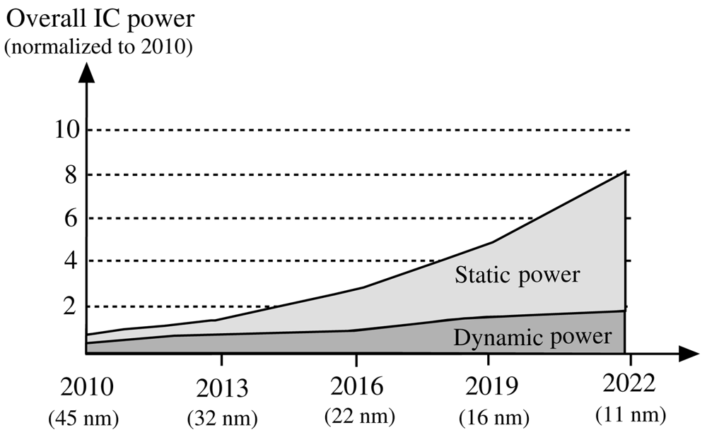
ITRS identifies leakage power consumption as “a clear long term threat and a focus topic for design technology in the next 15 years” [<xref ref-type="bibr" rid="b10-jlpea-01-00131">10</xref>]. Projections of the overall power dissipation within an IC are plotted in <xref ref-type="fig" rid="f1-jlpea-01-00131">Figure 1</xref> based on ITRS predictions.</p>
<p>The contribution of the static and dynamic power are separately highlighted, assuming a switching activity of 0.5 and constant clock frequency in each technology node. As illustrated in this figure, overall static power dominates dynamic power in deep submicrometer CMOS technologies. High variability of the leakage current due to process variations further exacerbates this issue [<xref ref-type="bibr" rid="b11-jlpea-01-00131">11</xref>].</p>
<p>The development of alternative gate dielectric materials with higher permittivity, <italic>i.e.</italic>, high-K dielectric, and metal gate transistors permit thicker dielectric layers, significantly reducing the gate leakage current [<xref ref-type="bibr" rid="b12-jlpea-01-00131">12</xref>,<xref ref-type="bibr" rid="b13-jlpea-01-00131">13</xref>]. The continuation of technology scaling below 45 nm have been possible partly due to this progress at the device level. As the gate leakage current has been significantly reduced, subthreshold leakage has become the dominant component for static power dissipation.</p>
<p>Various methodologies have been proposed to alleviate subthreshold leakage current consumption such as multi-threshold voltage CMOS (MTCMOS), also referred to as power gating [<xref ref-type="bibr" rid="b14-jlpea-01-00131">14</xref>], dynamic adjustment of the threshold voltage through body biasing [<xref ref-type="bibr" rid="b15-jlpea-01-00131">15</xref>], and multi-threshold voltage transistors, also referred to as dual threshold voltage (dual-<italic>V<sub>th</sub></italic>) partitioning [<xref ref-type="bibr" rid="b16-jlpea-01-00131">16</xref>]. These existing approaches have several limitations, particularly for low leakage register design, as further described in Section 3.</p>
<p>A comprehensive methodology is proposed in this paper to design path specific dual-<italic>V<sub>th</sub></italic>, low leakage registers while simultaneously considering clock-to-Q delay, setup time, hold time, type of timing path (short or long), and type of register (launching or capturing). Existing dual-<italic>V<sub>th</sub></italic> based registers reduce the leakage current only along the feedback path to not affect the timing constraints [<xref ref-type="bibr" rid="b17-jlpea-01-00131">17</xref>–<xref ref-type="bibr" rid="b19-jlpea-01-00131">19</xref>]. This traditional approach significantly limits the amount of leakage that can be reduced, particularly in sub 22 nm CMOS technologies. Furthermore, in conventional approaches, the hold time of the register may be affected which may produce a timing violation depending upon the type of timing path and register. These limitations of the existing approaches are overcome with the proposed design methodology while significantly increasing the amount of leakage current that is reduced.</p>
<p>The rest of the paper is organized as follows. Exiting multi-threshold voltage based leakage reduction techniques are summarized in Section 2. Background material reviewing different types of timing paths and timing constraints of a register are provided in Section 3. A methodology is described in Section 4 to design path specific registers with low leakage current. The results are discussed in Section 5. Finally, the paper is concluded in Section 6.</p></sec>
<sec>
<label>2.</label>
<title>Previous Work</title>
<p>Existing techniques to reduce leakage current are summarized in this section with an emphasis on multi-threshold voltage design. Related limitations of these techniques are also discussed.</p>
<p>
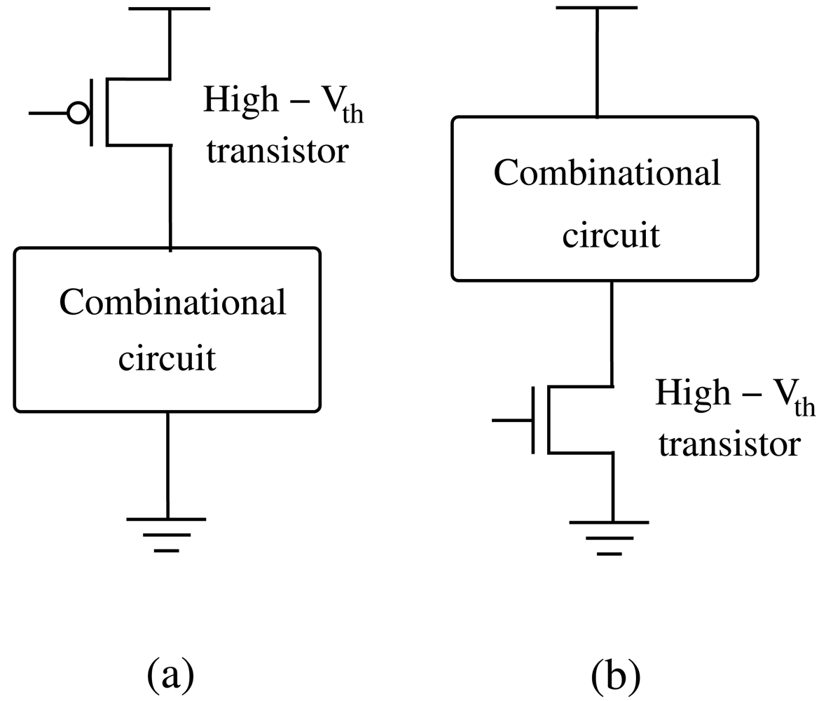
MTCMOS is a commonly used leakage reduction technique where a high threshold voltage (high-<italic>V<sub>th</sub></italic>) sleep transistor is placed between the circuit and power supply and/or ground node, as shown in <xref ref-type="fig" rid="f2-jlpea-01-00131">Figure 2</xref>.</p>
<p>When the circuit operates in the idle mode, high-<italic>V<sub>th</sub></italic> sleep transistor is cutoff, disconnecting the circuit from the power supply voltage and/or ground node. During the active mode, the sleep transistor is on and the combinational circuit consisting of low threshold voltage (low-<italic>V<sub>th</sub></italic>) transistors operates normally. The drain of the sleep transistor is referred to as virtual power (if the sleep transistor is placed between the circuit and power supply) and virtual ground (if the sleep transistor is placed between the circuit and ground node). Subthreshold leakage current is reduced during the idle mode since the sleep transistor behaves as a large resistance between the combinational circuit and power supply and/or ground node.</p>
<p>There are however several limitations of MTCMOS. When the mode of operation changes from idle to active, the circuit requires a specific amount of time to charge the virtual power node or discharge the virtual ground node. This required time is referred to as wake up latency [<xref ref-type="bibr" rid="b20-jlpea-01-00131">20</xref>]. Several clock cycles are typically required for the virtual ground or power to stabilize. Furthermore, the circuit may experience ground bounce during this time, affecting the reliable operation of nearby logic circuits.</p>
<p>Another limitation of MTCMOS that is more related to this paper is its application to memory elements such as a register. MTCMOS cannot be directly applied to a register since the state of the register should be preserved even when the register is in the idle mode. In conventional MTCMOS, however, the idle circuit is disconnected from the power supply voltage and the state of the circuit is lost. Several different versions of MTCMOS have been developed specifically for register design to alleviate this issue [<xref ref-type="bibr" rid="b8-jlpea-01-00131">8</xref>,<xref ref-type="bibr" rid="b14-jlpea-01-00131">14</xref>,<xref ref-type="bibr" rid="b21-jlpea-01-00131">21</xref>–<xref ref-type="bibr" rid="b23-jlpea-01-00131">23</xref>]. These techniques, however, require additional inverters and transmission gates, decreasing the amount of power that can be reduced while also increasing the overall area.</p>
<p>Exploiting the dependence of the threshold voltage on bulk potential has also been proposed to dynamically adjust the threshold voltage, referred to as adaptive body biasing [<xref ref-type="bibr" rid="b15-jlpea-01-00131">15</xref>]. During idle mode, the substrate of the circuit is reverse biased to increase the threshold voltage, thereby reducing the leakage current. The primary drawback of this methodology is to generate the bias voltage for the substrate in a power efficient way. A control circuitry is also required, further decreasing the power efficiency.</p>
<p>
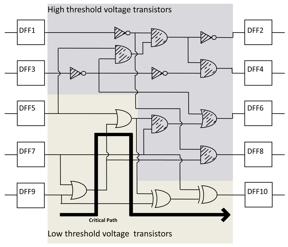
Another technique to reduce the leakage current is based on utilizing the multi-threshold voltage transistors that are provided by the manufacturing technology. This technique is also referred to as dual-<italic>V<sub>th</sub></italic> partitioning [<xref ref-type="bibr" rid="b24-jlpea-01-00131">24</xref>]. Those logic gates that are not part of the critical path are replaced with high-<italic>V<sub>th</sub></italic> transistors to reduce the leakage current by exploiting the excessive slack. Alternatively, those gates along the critical path are implemented with low-<italic>V<sub>th</sub></italic> transistors to satisfy the timing constraints, as depicted in <xref ref-type="fig" rid="f3-jlpea-01-00131">Figure 3</xref>.</p>
<p>A similar approach has been developed to design the registers. Those transistors that are not located along the clock-to-Q delay path have been replaced with high-<italic>V<sub>th</sub></italic> devices to reduce the leakage current within a register [<xref ref-type="bibr" rid="b17-jlpea-01-00131">17</xref>–<xref ref-type="bibr" rid="b19-jlpea-01-00131">19</xref>]. Unfortunately, in these existing approaches, the number of high-<italic>V<sub>th</sub></italic> transistors is sufficiently small, limiting the overall reduction in the leakage current. Furthermore, since these transistors are not located along the clock-to-Q delay path, the size of these transistors is typically small. Alternatively, those transistors that are located along the clock-to-Q delay path are typically sized larger, making leakage current more significant in these transistors. Another important limitation of the existing approaches is the inability to consider important timing constraints such as setup and hold times. The type of timing path, <italic>i.e.</italic>, short or long, and the type of register, <italic>i.e.,</italic> launching or capturing, significantly affect the design process of low leakage registers, as demonstrated in this paper. Ignoring these effects not only decreases the amount of leakage current that can be reduced, but may also affect reliable circuit operation since the timing constraints may be violated. Thus, application of dual-<italic>V<sub>th</sub></italic> partitioning to the design process of a register requires additional attention. A methodology is proposed in this paper to design dual-<italic>V<sub>th</sub></italic>, low leakage registers by simultaneously considering the clock-to-Q delay, setup time, hold time, and the type of register and timing path. The simultaneous consideration of these parameters is critical to exploit multi-threshold voltage transistors and to guarantee system functionality and timing in deep submicrometer CMOS technologies.</p></sec>
<sec>
<label>3.</label>
<title>Background</title>
<p>Timing characteristics of synchronous systems are briefly introduced in Section 3.1. The timing constraints of a register, <italic>i.e.</italic>, setup and hold times, are reviewed in Section 3.2.</p>
<sec>
<label>3.1.</label>
<title>Timing Characteristics of Synchronous Systems</title>
<p>A simple synchronous digital circuit consisting of two sequentially-adjacent registers with a combinational circuit between these registers is shown in <xref ref-type="fig" rid="f4-jlpea-01-00131">Figure 4</xref>.</p>
<p>The first register is referred to as <italic>launching register</italic> whereas the second register is called <italic>capturing register</italic>.</p>
<p>Two inequalities should be satisfied for this circuit to function properly [<xref ref-type="bibr" rid="b25-jlpea-01-00131">25</xref>]. Referring to <xref ref-type="fig" rid="f4-jlpea-01-00131">Figure 4</xref>, the first inequality is
<disp-formula id="FD1">
<label>(1)</label>
<mml:math id="mm1" display="block">
<mml:semantics id="sm1">
<mml:mrow>
<mml:msub>
<mml:mi>T</mml:mi>
<mml:mrow>
<mml:mi mathvariant="italic">Cf</mml:mi></mml:mrow></mml:msub>
<mml:mo>+</mml:mo>
<mml:msub>
<mml:mi>T</mml:mi>
<mml:mrow>
<mml:mi mathvariant="italic">CP</mml:mi></mml:mrow></mml:msub>
<mml:mo>≥</mml:mo>
<mml:msub>
<mml:mi>T</mml:mi>
<mml:mrow>
<mml:mi mathvariant="italic">Ci</mml:mi></mml:mrow></mml:msub>
<mml:mo>+</mml:mo>
<mml:msub>
<mml:mi>T</mml:mi>
<mml:mi mathvariant="italic">D</mml:mi></mml:msub>
<mml:mo>+</mml:mo>
<mml:msub>
<mml:mi>T</mml:mi>
<mml:mi mathvariant="italic">S</mml:mi></mml:msub>
<mml:mo> </mml:mo>
<mml:mrow/></mml:mrow></mml:semantics></mml:math></disp-formula>where <italic>T<sub>Ci</sub></italic> and <italic>T<sub>Cf</sub></italic> are the delay for the clock signals to arrive, respectively, at the launching and capturing registers. Note that <italic>T<sub>Ci</sub></italic> and <italic>T<sub>Cf</sub></italic> are also referred to as, respectively, the delay of the clock launch path and clock capture path. <italic>T<sub>CP</sub></italic> is the clock period. <italic>T<sub>D</sub></italic> is the data path delay consisting of the clock-to-Q delay of the launching register, logic delay of the combinational circuit, and the interconnect delay. <italic>T<sub>S</sub></italic> is the setup time of the capturing register. Note that (<xref ref-type="disp-formula" rid="FD1">1</xref>) determines the maximum speed of the circuit, making this inequality important for critical paths.</p>
<p>The second inequality that needs to be satisfied is
<disp-formula id="FD2">
<label>(2)</label>
<mml:math id="mm2" display="block">
<mml:semantics id="sm2">
<mml:mrow>
<mml:msub>
<mml:mi>T</mml:mi>
<mml:mrow>
<mml:mi mathvariant="italic">Ci</mml:mi></mml:mrow></mml:msub>
<mml:mo>+</mml:mo>
<mml:msub>
<mml:mi>T</mml:mi>
<mml:mi>D</mml:mi></mml:msub>
<mml:mo>≥</mml:mo>
<mml:msub>
<mml:mi>T</mml:mi>
<mml:mrow>
<mml:mi mathvariant="italic">Cf</mml:mi></mml:mrow></mml:msub>
<mml:mo>+</mml:mo>
<mml:msub>
<mml:mi>T</mml:mi>
<mml:mi>H</mml:mi></mml:msub></mml:mrow></mml:semantics></mml:math></disp-formula>where <italic>T<sub>H</sub></italic> is the hold time of the capturing register. This inequality guarantees that no race condition exists, <italic>i.e.</italic>, the data is not latched to the final register within the same clock edge. Note that (2) is relatively more important for those timing paths where the data path delay is small, <italic>i.e.</italic>, short paths, such as a shift register or counter.</p>
<p>These inequalities, the type of data path (short <italic>versus</italic> long), and the type of register (launching and capturing) play an important role in the design of low leakage, dual-<italic>V<sub>th</sub></italic> registers, as described in Section 4. The timing constraints of a register and related circuit level issues are described in the following section.</p></sec>
<sec>
<label>3.2.</label>
<title>Timing Constraints of a Register</title>
<p>Inequalities (<xref ref-type="disp-formula" rid="FD1">1</xref>) and (<xref ref-type="disp-formula" rid="FD2">2</xref>) require a difference called a <italic>skew</italic> to be larger than or equal to a <italic>timing constraint.</italic> These inequalities, therefore, can be rewritten as [<xref ref-type="bibr" rid="b25-jlpea-01-00131">25</xref>]
<disp-formula id="FD3">
<label>(3)</label>
<mml:math id="mm3" display="block">
<mml:semantics id="sm3">
<mml:mrow>
<mml:mtext>Setup skew</mml:mtext>
<mml:mo>≥</mml:mo>
<mml:msub>
<mml:mi>T</mml:mi>
<mml:mi>S</mml:mi></mml:msub></mml:mrow></mml:semantics></mml:math></disp-formula>
<disp-formula id="FD4">
<label>(4)</label>
<mml:math id="mm4" display="block">
<mml:semantics id="sm4">
<mml:mrow>
<mml:mtext>Hold skew</mml:mtext>
<mml:mo>≥</mml:mo>
<mml:msub>
<mml:mi>T</mml:mi>
<mml:mi>H</mml:mi></mml:msub></mml:mrow></mml:semantics></mml:math></disp-formula>where the setup skew and hold skew are, respectively
<disp-formula id="FD5">
<label>(5)</label>
<mml:math id="mm5" display="block">
<mml:semantics id="sm5">
<mml:mrow>
<mml:mtext>Setup skew</mml:mtext>
<mml:mo>=</mml:mo>
<mml:msub>
<mml:mi>T</mml:mi>
<mml:mrow>
<mml:mi mathvariant="italic">Cf</mml:mi></mml:mrow></mml:msub>
<mml:mo>+</mml:mo>
<mml:msub>
<mml:mi>T</mml:mi>
<mml:mrow>
<mml:mi mathvariant="italic">CP</mml:mi></mml:mrow></mml:msub>
<mml:mo>−</mml:mo>
<mml:mrow>
<mml:mo stretchy="false">(</mml:mo>
<mml:mrow>
<mml:msub>
<mml:mi>T</mml:mi>
<mml:mrow>
<mml:mi mathvariant="italic">Ci</mml:mi></mml:mrow></mml:msub>
<mml:mo>+</mml:mo>
<mml:msub>
<mml:mi>T</mml:mi>
<mml:mi>D</mml:mi></mml:msub></mml:mrow>
<mml:mo stretchy="false">)</mml:mo></mml:mrow></mml:mrow></mml:semantics></mml:math></disp-formula>
<disp-formula id="FD6">
<label>(6)</label>
<mml:math id="mm6" display="block">
<mml:semantics id="sm6">
<mml:mrow>
<mml:mi>Hold Skew</mml:mi>
<mml:mo>=</mml:mo>
<mml:msub>
<mml:mi>T</mml:mi>
<mml:mrow>
<mml:mi mathvariant="italic">Ci</mml:mi></mml:mrow></mml:msub>
<mml:mo>+</mml:mo>
<mml:msub>
<mml:mi>T</mml:mi>
<mml:mi>D</mml:mi></mml:msub>
<mml:mo>−</mml:mo>
<mml:msub>
<mml:mi>T</mml:mi>
<mml:mrow>
<mml:mi mathvariant="italic">Cf</mml:mi></mml:mrow></mml:msub></mml:mrow></mml:semantics></mml:math></disp-formula> Note the important difference between setup-hold skews and setup-hold times: Setup and hold skews refer to <italic>any</italic> time difference between the data and clock signals whereas the setup and hold times refer to the minimum required time difference to reliably capture and store the data.</p>
<p>
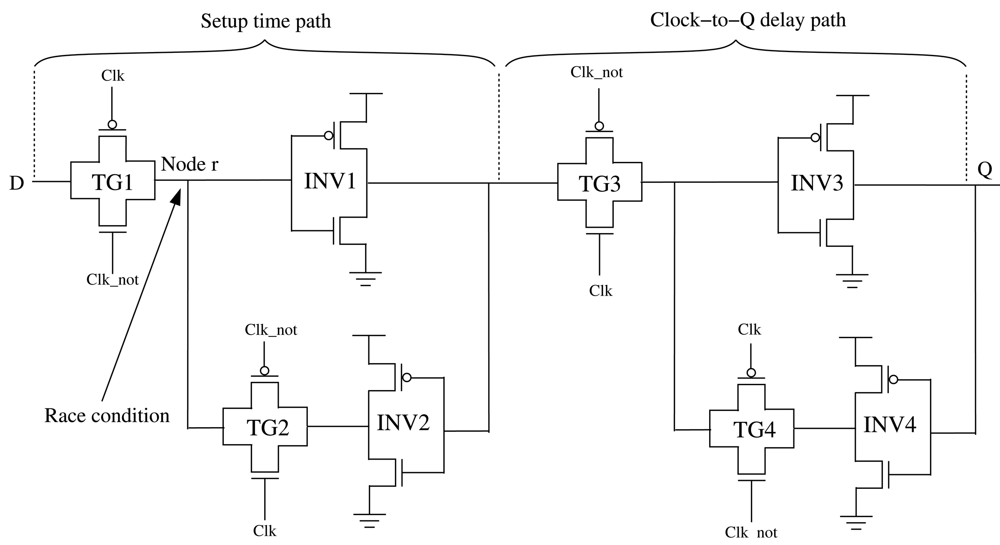
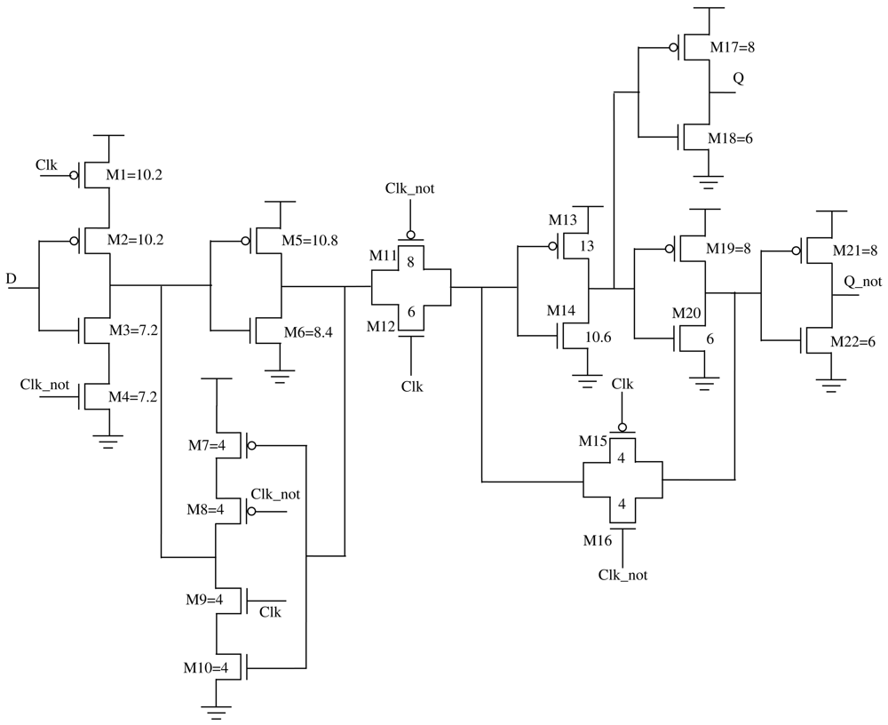
Transistor level realization of a widely used master slave type, edge triggered register is illustrated in <xref ref-type="fig" rid="f5-jlpea-01-00131">Figure 5</xref>.</p>
<p>According to the setup time constraint, the data signal should be stable at the input of a register for a sufficient amount of time before the active edge of the clock signal. In the example shown in <xref ref-type="fig" rid="f5-jlpea-01-00131">Figure 5</xref>, the active edge is a low-to-high transition of the clock signal since the data propagates to the output after this transition. Setup time guarantees that the data is reliably latched to the master before the rising edge of the clock signal arrives. Ideally, the data signal should propagate through TG1 and INV1, arriving at the output of INV1 before the rising edge of the clock signal. According to this condition, the path that determines the setup time consists of TG1 and INV1, as depicted in
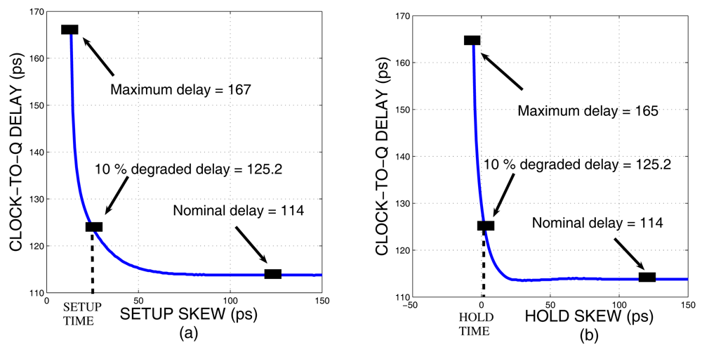
 <xref ref-type="fig" rid="f5-jlpea-01-00131">Figure 5</xref>. This condition, however, may require a relatively large setup time. A conventional technique to characterize the setup time constraint of a register is to examine the setup skew <italic>versus</italic> clock-to-Q delay relationship, as shown in <xref ref-type="fig" rid="f6-jlpea-01-00131">Figure 6(a)</xref> [<xref ref-type="bibr" rid="b25-jlpea-01-00131">25</xref>–<xref ref-type="bibr" rid="b27-jlpea-01-00131">27</xref>].</p>
<p>The smallest setup skew that corresponds to the nominal clock-to-Q delay is approximately equal to the summation of the two delays: TG1 and INV1. As the setup skew is further reduced, clock-to-Q delay gradually increases since for smaller setup skews, the data signal cannot reach to the output of INV1. After a specific point, the clock-to-Q delay starts to exponentially increase due to a race condition at node <italic>r</italic> since this node is simultaneously driven by two gates: TG1 and TG2. The race condition occurs between the new data driven by TG1 and old data driven by TG2. This region is referred to as metastable and therefore avoided during the characterization process. Typically, a 10% degradation in clock-to-Q delay is allowed while characterizing the setup time, as shown in <xref ref-type="fig" rid="f6-jlpea-01-00131">Figure 6(a)</xref>.</p>
<p>According to the hold time constraint, the data signal should be stable at the input of a register for a sufficient amount of time after the active edge of the clock signal. This constraint is due to non-ideal characteristics of TG1 as a switch. If the hold time constraint is not satisfied, the new data can be latched into the register and overwrite the previous valid data during the same clock cycle. Note that hold time can sometimes be smaller than zero. In this case, even if the new data propagates through TG1, a race condition exists at node <italic>r</italic> between the new and old data. If the old data succeeds over the new data, the register works correctly and the negative hold time is valid. The hold time constraint is therefore partly determined by the relative drive strengths of TG1 and TG2. Note that, if the hold time is further reduced, the clock-to-Q delay exponentially increases, as shown in <xref ref-type="fig" rid="f6-jlpea-01-00131">Figure 6(b)</xref>. Similar to setup time characterization, a 10% degradation in clock-to-Q delay is allowed while characterizing the hold time.</p>
<p>These timing constraints (setup and hold times) and clock-to-Q delay play an important role in the design process of low leakage, dual-<italic>V<sub>th</sub></italic> registers. When specific transistors within a register are replaced with high-<italic>V<sub>th</sub></italic> devices to reduce leakage current, the timing constraints may change. Ignoring this effect may produce timing violations, causing a degradation in clock frequency or functional failure. The proposed methodology overcomes this limitation, as described in the following section.</p></sec></sec>
<sec>
<label>4.</label>
<title>Proposed Methodology</title>
<p>As described in Section 2, existing work on dual-<italic>V<sub>th</sub></italic> based register design does not consider different types of data paths and registers. Referring to <xref ref-type="fig" rid="f5-jlpea-01-00131">Figure 5</xref>, a typical approach is to design TG1, INV1, TG3, and INV3 with low-<italic>V<sub>th</sub></italic> transistors to improve the setup time and clock-to-Q delay. The remaining inverters and transmission gates that are located along the feedback path are designed with high-<italic>V</italic><sub>th</sub> devices to minimize the leakage current. This approach, however, is not practical for all of the timing paths. For example, in a short path, reduced clock-to-Q delay may not be desirable according to the second inequality determined by (2). The amount leakage current that can be reduced is also limited since all of the transistors located along the forward signal path, <italic>i.e.</italic>, within TG1, INV1, TG3, and INV3, are low-<italic>V<sub>th</sub></italic> devices. Note that these transistors are typically sized larger to minimize clock-to-Q delay and setup time. The leakage current is therefore relatively more important for these transistors as compared to those that are located along the feedback paths.</p>
<p>The design process of a dual-<italic>V<sub>th</sub></italic>, low leakage register is therefore strongly dependent upon the type of data path, <italic>i.e.</italic>, long (critical), noncritical, and short; and type of register, <italic>i.e.</italic>, launching or capturing, as illustrated in <xref ref-type="fig" rid="f4-jlpea-01-00131">Figure 4</xref>. Three different types of dual-<italic>V<sub>th</sub></italic> registers that consider these dependencies are proposed in this paper, as described in Section 4.1. Assigning the proper threshold voltage to each transistor within these registers are discussed in Section 4.2. The amount of leakage that can be reduced by utilizing the proposed registers is evaluated in Section 4.3. Finally, simulation results based on three ISCAS 89 benchmark circuits are provided in Section 4.4.</p>
<sec>
<label>4.1.</label>
<title>Path Specific Dual-V<sub>th</sub> Register Design</title>
<p>The type of timing path and register should be considered during the design process of a dual-<italic>V<sub>th</sub></italic>, low leakage register. Consider, for example, a launching register in a noncritical or short path. In this case, clock-to-Q delay of the register is not critical and therefore can be traded to reduce leakage current. Similarly, for a a capturing register in a noncritical or short path, (<xref ref-type="disp-formula" rid="FD2">2</xref>) is the important inequality and the setup time of this register is not critical. Setup time therefore can be traded to achieve low leakage in a capturing register of a noncritical or short path. Existing techniques cannot utilize this opportunity since the transistors located along the clock-to-Q delay and setup path are realized with low-<italic>V<sub>th</sub></italic> devices. Finally, consider a capturing register in a critical path. In this case, the hold time is not critical since (<xref ref-type="disp-formula" rid="FD1">1</xref>) is the important constraint. Hold time therefore can be traded to achieve low leakage in a capturing register of a critical or long path. Additional constraints, however, exist for each of these three cases to guarantee that both (<xref ref-type="disp-formula" rid="FD1">1</xref>) and (<xref ref-type="disp-formula" rid="FD2">2</xref>) are satisfied after specific transistors are replaced with high-<italic>V<sub>th</sub></italic> devices.</p>
<p>Three different types of dual-<italic>V<sub>th</sub></italic> registers are proposed depending on the type of data path and register, as summarized in <xref ref-type="table" rid="t1-jlpea-01-00131">Table 1</xref> and described in the following:</p></sec>
<sec>
<title>Register 1</title>
<p>This register is designed to replace launching registers in noncritical or short paths. Since there is excessive setup slack in noncritical paths, the primary objective is to trade clock-to-Q delay for leakage current. Both setup and hold times of the register, however, should remain the same (or be reduced) since this register behaves as a capturing register for the previous data path, which may be a critical or short path. Thus, to guarantee that the timing characteristics of the previous path are not affected, the setup and hold times of the register should not increase.</p></sec>
<sec>
<title>Register 2</title>
<p>This register is designed to replace capturing registers in noncritical or short paths. Due to excessive setup slack, the primary objective is to trade setup time for leakage current. The clock-to-Q delay of the register, however, should remain the same (or be reduced) since this register behaves as a launching register for the following data path, which may be a critical path. Furthermore, the hold time should also remain the same (or be reduced) since for a short data path, (
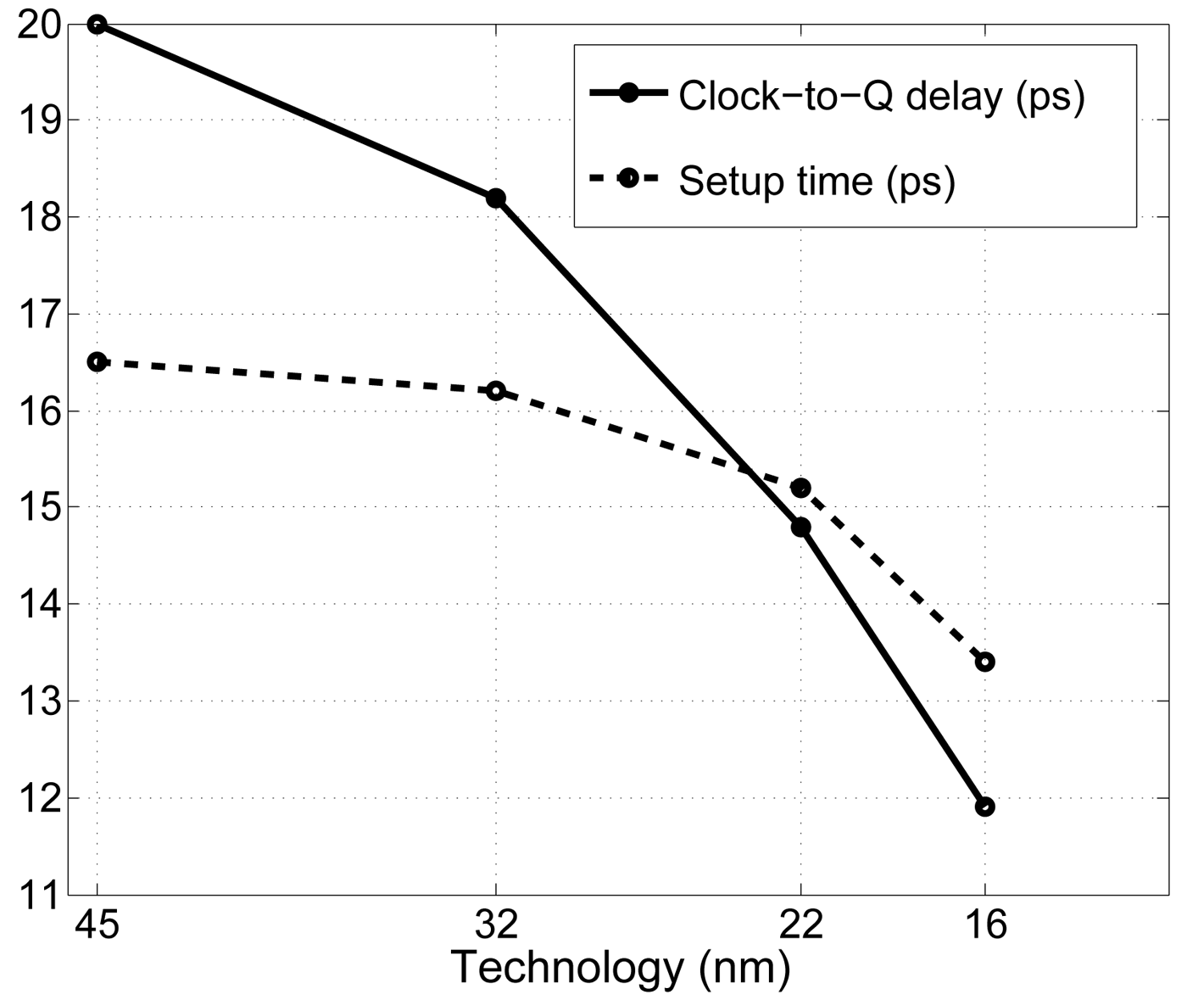
<xref ref-type="disp-formula" rid="FD2">2</xref>) is critical. Note that this second register is sufficiently effective to reduce leakage current since the setup time is relatively more important in advanced technologies, as shown in <xref ref-type="fig" rid="f7-jlpea-01-00131">Figure 7</xref>. According to this figure, starting 22 nm technology, setup time of the register is higher than the clock-to-Q delay. Thus, the opportunity to trade setup time for leakage current should not be overlooked. Note that the setup time has been characterized using the procedure described in Section 3.2.</p></sec>
<sec>
<title>Register 3</title>
<p>The third register is designed to replace capturing registers in critical paths. The primary objective is to trade hold time for leakage current since in a critical path, (<xref ref-type="disp-formula" rid="FD1">1</xref>) is important and hold slack is typically large. The clock-to-Q delay should remain the same (or be reduced) since the register behaves as a launching register for the following data path, which may also be a critical path. Furthermore, the setup time should also remain the same (or be reduced) since for a critical path, (<xref ref-type="disp-formula" rid="FD1">1</xref>) is important.</p></sec>
<sec>
<label>4.2.</label>
<title>Threshold Voltage Assignment</title>
<p>An edge triggered D type flip-flop with 2X drive capability is chosen from an industrial standard cell library. The transistor level schematic of the register is illustrated in <xref ref-type="fig" rid="f8-jlpea-01-00131">Figure 8</xref>, including the <italic>W/L</italic> ratios of each transistor.</p>
<p>Note that in the master latch, a tristate inverter is used that combines the TG1 and INV1 of <xref ref-type="fig" rid="f5-jlpea-01-00131">Figure 5</xref>. Similarly, the feedback of the master latch also utilizes a tristate inverter. This schematic and <italic>W/L</italic> ratios are used in the simulations without any modification.</p>
<p>In the original version, the register shown in <xref ref-type="fig" rid="f8-jlpea-01-00131">Figure 8</xref> is designed using only low-<italic>V<sub>th</sub></italic> transistors. To design <italic>Register 1</italic>, high-<italic>V<sub>th</sub></italic> devices are used for those transistors located along the clock-to-Q delay path, <italic>i.e.,</italic> M13, M14, M17, M18, M19, M20, M21, and M22. Clock-to-Q delay is therefore traded to reduce leakage current. Note that, the setup and hold times of the register remain the same since these transistor do not affect the timing constraints of the register.</p>
<p>To design <italic>Register 2</italic>, high-<italic>V<sub>th</sub></italic> transistors are used only for M2 and M3 to trade setup time for leakage current. Note that M5 and M6 are designed using low-<italic>V<sub>th</sub></italic> transistors even though this inverter is along the setup path, as illustrated in <xref ref-type="fig" rid="f5-jlpea-01-00131">Figure 5</xref>. However, as described in the previous section, clock-to-Q delay and hold time of the register should remain the same. Replacing M5 and M6 with high-<italic>V</italic><sub>th</sub> transistors affects the clock-to-Q delay since this inverter drives the input of the slave latch.</p>
<p>Finally, to design <italic>Register 3</italic>, high-<italic>V<sub>th</sub></italic> transistors are used for M7, M8, M9, and M10 to trade hold time for leakage current. Note that the feedback path becomes weaker due to high-<italic>V<sub>th</sub></italic> transistors. As such, hold time increases since it is more difficult for the old data to overwrite the new data at the output of the first gate, thereby requiring a larger hold time constraint. Low-<italic>V<sub>th</sub></italic> devices are used for the remaining transistors to guarantee that the clock-to-Q delay and setup time remain the same. For example, M1, M2, M3, and M4 directly affect the setup time constraint and therefore designed with low-<italic>V<sub>th</sub></italic> transistors. Threshold voltage assignment of all of the transistors are listed in <xref ref-type="table" rid="t2-jlpea-01-00131">Table 2</xref> for each register.</p></sec>
<sec>
<label>4.3.</label>
<title>Reduction in the Leakage Current</title>
<p>The amount of reduction in the leakage current achieved by utilizing the proposed three registers is evaluated in this section. Four CMOS technology generations, 45 nm, 32 nm, 22 nm, and 16 nm, are considered using a predictive technology model [<xref ref-type="bibr" rid="b28-jlpea-01-00131">28</xref>,<xref ref-type="bibr" rid="b29-jlpea-01-00131">29</xref>].</p>
<p>The register illustrated in <xref ref-type="fig" rid="f8-jlpea-01-00131">Figure 8</xref> is simulated for each technology node where the <italic>W/L</italic> ratios of the transistors are maintained constant. The leakage current drawn from the power supply is evaluated for the three registers and the results are compared with the leakage current of the original register where only low-<italic>V<sub>th</sub></italic> transistors are used.</p>
<p>
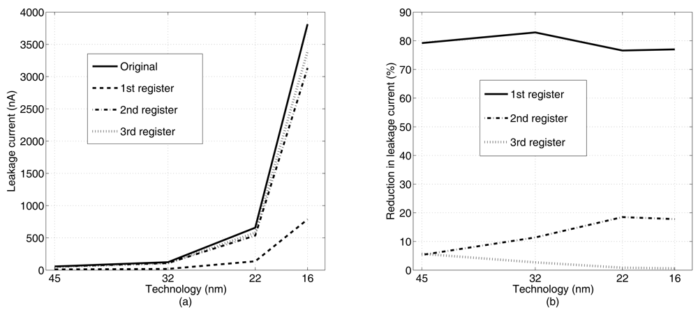
The results are illustrated in <xref ref-type="fig" rid="f9-jlpea-01-00131">Figure 9</xref>. Note that for the first register, the state of the clock signal does not change the results since all of the high-<italic>V<sub>th</sub></italic> transistors are within the slave latch. For the second and third registers, however, high-<italic>V<sub>th</sub></italic> transistors exist within the tristate inverters. The state of the clock signal is therefore important in evaluating the results. For example, for the second register, clock signal should be at <italic>V<sub>SS</sub></italic> to guarantee that the initial tristate inverter is not in the high impedance state. Similarly, for the third register, clock signal should be at <italic>V<sub>DD</sub></italic> so that the second tristate inverter located along the feedback path is not in the high impedance state. The leakage current of the original register is therefore compared with the first two registers and third register when the clock signal is, respectively, at <italic>V<sub>SS</sub></italic> and <italic>V<sub>DD</sub></italic>.</p>
<p>The leakage current increases with technology, exhibiting a large jump in the 16 nm node. A significant amount of reduction in the leakage current, 79% on average, is achieved by the first register since the number of high-<italic>V<sub>th</sub></italic> transistors is higher, as listed in <xref ref-type="table" rid="t2-jlpea-01-00131">Table 2</xref>. The second register also achieves a considerable amount of reduction in the leakage current, 13% on average and higher below 32 nm technology nodes, since the importance of setup time has been increasing with technology, as depicted in <xref ref-type="fig" rid="f7-jlpea-01-00131">Figure 7</xref>. The reduction in the leakage current obtained by the third register is relatively smaller, as further discussed in Section 5. All of the results are listed in <xref ref-type="table" rid="t3-jlpea-01-00131">Table 3</xref> where the absolute reduction in the leakage current is also provided for each case.</p>
<p>The timing constraints (setup and hold times) and clock-to-Q delay of the three registers are characterized as described in Section 3.2. As listed in <xref ref-type="table" rid="t4-jlpea-01-00131">Table 4</xref>, all of the three registers satisfy the required timing constraints listed previously in <xref ref-type="table" rid="t1-jlpea-01-00131">Table 1</xref>.</p>
<p>Specifically, for the first register, setup and hold times are slightly reduced as compared to the original register whereas clock-to-Q delay increases, on average, by 24.6 ps to improve the leakage current. The required condition is therefore satisfied since the setup and hold times do not increase. For the second register, setup time increases, on average, by 13.3 ps to reduce the leakage current. Alternatively, clock-to-Q delay remains the same whereas hold time is reduced, thereby satisfying the required condition. Note that the hold time is reduced since M2 and M3 are high-<italic>V<sub>th</sub></italic> transistors in this register. It is therefore more difficult for the input data to propagate to the output of the first tristate inverter, requiring a shorter hold time. For the third register, setup time and clock-to-Q delay remain approximately the same whereas hold time increases, on average, by 1.7 ps to reduce the leakage current. The last register therefore also satisfies the required timing constraints.</p></sec>
<sec sec-type="results">
<label>4.4.</label>
<title>Simulation Results</title>
<p>Three ISCAS 89 benchmark circuits, s27, s526, and s1423, are utilized in this section to better evaluate the efficacy of the proposed methodology on functional circuits rather than only on a register [<xref ref-type="bibr" rid="b30-jlpea-01-00131">30</xref>]. The total number of gates in these sequential circuits is, respectively, 8, 141, and 490 whereas the total number of registers is, respectively, 3, 21, and 74.</p>
<p>First, the leakage current of the circuits is analyzed when the registers are designed only with low-<italic>V<sub>th</sub></italic> transistors. In the second step, registers within each sequential circuit is replaced with the proposed registers based on the type of timing path. Since the critical paths are typically a small percentage of the overall circuit, <italic>Register 1</italic> and <italic>Register 2</italic> can be effectively utilized to trade, respectively, clock-to-Q delay and setup time for leakage power. In the last step, the methodology proposed in [<xref ref-type="bibr" rid="b17-jlpea-01-00131">17</xref>–<xref ref-type="bibr" rid="b19-jlpea-01-00131">19</xref>] is evaluated by replacing the low-<italic>V<sub>th</sub></italic> transistors along the feedback path of a register (M7 to M10, M15, and M16 in <xref ref-type="fig" rid="f5-jlpea-01-00131">Figure 5</xref>) with high-<italic>V<sub>th</sub></italic> transistors. The overall reduction in leakage current is compared for each case in four different technologies. Note that the register illustrated in <xref ref-type="fig" rid="f5-jlpea-01-00131">Figure 5</xref> is used for all of the circuits. Predictive device models are used for each technology [<xref ref-type="bibr" rid="b28-jlpea-01-00131">28</xref>,<xref ref-type="bibr" rid="b29-jlpea-01-00131">29</xref>]. The analysis is performed using H-SPICE [<xref ref-type="bibr" rid="b31-jlpea-01-00131">31</xref>].</p>
<p>The results of the analysis are listed in <xref ref-type="table" rid="t5-jlpea-01-00131">Table 5</xref>.</p>
<p>As summarized in this table, the proposed methodology achieves a significant reduction in the overall leakage current. Average reduction over three circuits and four technologies is approximately 23%. Note that the overall reduction in the leakage current increases as the size of the circuit grows and the ratio of the number of registers to the overall number of gates increases. Also note that according to these results, the reduction achieved by the methodology described in [<xref ref-type="bibr" rid="b17-jlpea-01-00131">17</xref>] is negligible due to two reasons: (1) As illustrated in <xref ref-type="fig" rid="f5-jlpea-01-00131">Figure 5</xref>, the feedback path of the master latch consists of a tristate inverter. Leakage current in a tristate inverter is significantly less than a regular inverter due to increased impedance between the power supply and ground; (2) The feedback path of the slave latch consists of only a transmission gate. The results provided in [<xref ref-type="bibr" rid="b17-jlpea-01-00131">17</xref>] assume a different register architecture, as shown in <xref ref-type="fig" rid="f8-jlpea-01-00131">Figure 8</xref>. For this architecture, there is an inverter along the feedback path of both master and slave latches, thereby increasing the overall reduction in leakage. In this work, the register is chosen from an industrial cell library without any modification. Note that the proposed methodology achieves a higher reduction in leakage current as compared to [<xref ref-type="bibr" rid="b17-jlpea-01-00131">17</xref>] even for the register shown in <xref ref-type="fig" rid="f8-jlpea-01-00131">Figure 8</xref> since the number of high-<italic>V<sub>th</sub></italic> transistors is higher in the proposed dual-<italic>V<sub>th</sub></italic> registers. Also note that the effect of high-<italic>V<sub>th</sub></italic> transistors on setup and hold times is not considered in [<xref ref-type="bibr" rid="b17-jlpea-01-00131">17</xref>]. This effect can be significant since an unexpected increase in the setup or hold times can produce a timing violation, as described in Section 4.2.</p></sec></sec>
<sec>
<label>5.</label>
<title>Discussion and Future Study</title>
<p>According to the results presented in the previous section, the first register achieves the highest amount of reduction due to two reasons: (1) greatest number of high-<italic>V<sub>th</sub></italic> transistors are used in this register and (2) the width of these transistors is relatively high to reduce the clock-to-Q delay. The second register also achieves a reasonable amount of reduction whereas the reduction achieved by the third register is small (2.5% on average) due to two reasons: (1) the stack effect within the tristate inverter increases the standby impedance between the power supply voltage and ground node and (2) since this tristate inverter is located along the feedback path, the width of the transistors is smaller, decreasing the leakage current. Note however that this leakage reduction is achieved without degrading the clock frequency. Area and dynamic power also remain the same. Furthermore, the absolute leakage reduction achieved by the third register is 20 nA in the 16 nm technology node. Even though the percent reduction is small, when a large number of registers is considered, the absolute reduction can become in the range of milliamperes. When the first two registers are also considered, the overall savings in the standby power consumption of a register significantly increase.</p>
<p>Also note that, three dual-<italic>V<sub>th</sub></italic> registers have been proposed, each for a specific type of timing path (critical or noncritical) and register (launching or capturing), as listed in <xref ref-type="table" rid="t1-jlpea-01-00131">Table 1</xref>. Two additional registers that achieve enhanced reduction in the leakage current can be designed based on the proposed registers. Consider, for example, the first proposed register (launching in a critical path) which behaves as a capturing register for the previous path. If the previous path is also noncritical, as depicted in <xref ref-type="fig" rid="f10-jlpea-01-00131">Figure 10</xref>, not only clock-to-Q delay, but also setup time can be traded to reduce the leakage current within this register.</p>
<p>In this case, the number of high-<italic>V<sub>th</sub></italic> transistors becomes higher, increasing the overall reduction in the leakage current. According to <xref ref-type="table" rid="t3-jlpea-01-00131">Table 3</xref>, the overall reduction, which corresponds to the summation of the reduction achieved by the first and second registers, exceeds 90% for sub 45 nm technology nodes. Alternatively, if the previous path is a critical path, not only clock-to-Q delay, but also hold time can be traded to reduce the leakage current. The overall reduction in this case is approximately equal to the summation of the reduction achieved by the first and third registers.</p>
<p>The primary disadvantage of the proposed methodology is the degradation in the robustness of a circuit. For example, the clock-to-Q delay of a launching register in a noncritical path is traded for the leakage current. Thus, the available timing slack of this data path is reduced. A reduced timing slack typically corresponds to a higher sensitivity to variations. The overall robustness is therefore degraded. Note however that this disadvantage is a common limitation in a large number of low power design techniques that rely on exploiting excessive slack.</p>
<p>Finally, also note that the results presented in this paper are based on a specific type of register. A similar methodology can be applied to other types of registers where clock-to-Q delay, setup, and hold times are traded to reduce the leakage current without affecting the clock frequency. The numerical results may change depending upon the transistor level design of a register. Effect of different register architectures on leakage reduction can therefore be investigated as future work. Application of the proposed methodology to pulsed latches also remains as a future study.</p></sec>
<sec>
<label>6.</label>
<title>Conclusions</title>
<p>A methodology has been proposed to design low leakage registers, minimizing standby power dissipation. Traditional dual-<italic>V<sub>th</sub></italic> registers utilize high-<italic>V<sub>th</sub></italic> transistors only along the feedback path of the master and slave latches where the overall reduction in leakage current is limited. As opposed to existing techniques, a register design methodology that considers the type of timing path (short or long) and register (launching and capturing) is developed. Three different dual-<italic>V<sub>th</sub></italic> registers are introduced where the first register trades clock-to-Q delay for leakage current, achieving, on average, 79% reduction in leakage current. The second and third registers trade, respectively, setup time and hold time to further reduce the leakage current. Depending on the type of timing paths, the overall reduction in the leakage current of a register can exceed 90%. Furthermore, an average reduction of 23% in leakage current is demonstrated for three ISCAS 89 benchmark circuits. Clock frequency and other design parameters such as area and dynamic power remain the same.</p></sec></body>
<back>
<sec sec-type="display-objects">
<title>Figures and Tables</title>
<fig id="f1-jlpea-01-00131" position="float">
<label>Figure 1.</label>
<caption>
<p>Projections of the IC overall power dissipation normalized to 45 nm technology node, highlighting the dominance of static power over dynamic power.</p></caption>
<graphic xlink:href="jlpea-01-00131f1.gif"/></fig>
<fig id="f2-jlpea-01-00131" position="float">
<label>Figure 2.</label>
<caption>
<p>Multi-threshold voltage CMOS (MTCMOS) design to reduce leakage current: (<bold>a</bold>) sleep transistor is placed between the circuit and power supply; (<bold>b</bold>) sleep transistor is placed between the circuit and ground node.</p></caption>
<graphic xlink:href="jlpea-01-00131f2.gif"/></fig>
<fig id="f3-jlpea-01-00131" position="float">
<label>Figure 3.</label>
<caption>
<p>Dual threshold voltage partitioning to reduce leakage current while maintaining clock frequency the same.</p></caption>
<graphic xlink:href="jlpea-01-00131f3.gif"/></fig>
<fig id="f4-jlpea-01-00131" position="float">
<label>Figure 4.</label>
<caption>
<p>Simple synchronous circuit consisting of a combinational logic and two types of registers: Launching and capturing.</p></caption>
<graphic xlink:href="jlpea-01-00131f4.gif"/></fig>
<fig id="f5-jlpea-01-00131" position="float">
<label>Figure 5.</label>
<caption>
<p>Transistor level schematic of a widely used master slave type edge triggered register, illustrating the paths for clock-to-Q delay and setup time.</p></caption>
<graphic xlink:href="jlpea-01-00131f5.gif"/></fig>
<fig id="f6-jlpea-01-00131" position="float">
<label>Figure 6.</label>
<caption>
<p>Timing constraint characterization for sequential cells: (<bold>a</bold>) setup skew <italic>versus</italic> clock-to-Q delay for setup time characterization, (<bold>b</bold>) hold skew <italic>versus</italic> clock-to-Q delay for hold time characterization.</p></caption>
<graphic xlink:href="jlpea-01-00131f6.gif"/></fig>
<fig id="f7-jlpea-01-00131" position="float">
<label>Figure 7.</label>
<caption>
<p>Dependence of clock-to-Q delay and setup time of a register on technology.</p></caption>
<graphic xlink:href="jlpea-01-00131f7.gif"/></fig>
<fig id="f8-jlpea-01-00131" position="float">
<label>Figure 8.</label>
<caption>
<p>Transistor level schematic of a master slave type, edge triggered register where the numbers represent the <italic>W/L</italic> ratio for each transistor. Three different dual-<italic>V<sub>th</sub></italic>, low leakage registers are designed based on this schematic.</p></caption>
<graphic xlink:href="jlpea-01-00131f8.gif"/></fig>
<fig id="f9-jlpea-01-00131" position="float">
<label>Figure 9.</label>
<caption>
<p>Comparison of leakage current obtained from the original and proposed registers for four technology nodes: (<bold>a</bold>) absolute leakage current; (<bold>b</bold>) percent reduction in the leakage current.</p></caption>
<graphic xlink:href="jlpea-01-00131f9.gif"/></fig>
<fig id="f10-jlpea-01-00131" position="float">
<label>Figure 10.</label>
<caption>
<p>Illustration of a register (R<sub>2</sub>) that simultaneously behaves as a launching register of a noncritical path and a capturing register of the previous noncritical path.</p></caption>
<graphic xlink:href="jlpea-01-00131f10.gif"/></fig>
<table-wrap id="t1-jlpea-01-00131" position="float">
<label>Table 1.</label>
<caption>
<p>Timing characteristics of the proposed dual-<italic>V<sub>th</sub></italic> registers.</p></caption>
<table frame="hsides" rules="groups">
<thead>
<tr>
<th align="left" valign="top"/>
<th align="left" valign="top"><bold>Timing Path</bold></th>
<th align="left" valign="top"><bold>Register Type</bold></th>
<th align="left" valign="top"><bold>Clock-to-Q Delay</bold></th>
<th align="left" valign="top"><bold>Setup Time</bold></th>
<th align="left" valign="top"><bold>Hold Time</bold></th></tr></thead>
<tbody>
<tr>
<td align="left" valign="top"><italic>Register 1</italic></td>
<td align="left" valign="top">Noncritical</td>
<td align="left" valign="top">Launching</td>
<td align="left" valign="top">Larger</td>
<td align="left" valign="top">Same or less</td>
<td align="left" valign="top">Same or less</td></tr>
<tr>
<td align="left" valign="top"><italic>Register 2</italic></td>
<td align="left" valign="top">Noncritical</td>
<td align="left" valign="top">Capturing</td>
<td align="left" valign="top">Same or less</td>
<td align="left" valign="top">Larger</td>
<td align="left" valign="top">Same or less</td></tr>
<tr>
<td align="left" valign="top"><italic>Register 3</italic></td>
<td align="left" valign="top">Critical</td>
<td align="left" valign="top">Capturing</td>
<td align="left" valign="top">Same or less</td>
<td align="left" valign="top">Larger</td></tr></tbody></table></table-wrap>
<table-wrap id="t2-jlpea-01-00131" position="float">
<label>Table 2.</label>
<caption>
<p>Threshold voltage assignment of the three proposed registers.</p></caption>
<table frame="hsides" rules="groups">
<thead>
<tr>
<th align="left" valign="top"/>
<th align="left" valign="top"><italic><bold>Register 1</bold></italic></th>
<th align="left" valign="top"><italic><bold>Register 2</bold></italic></th>
<th align="left" valign="top"><italic><bold>Register 3</bold></italic></th></tr></thead>
<tbody>
<tr>
<td align="left" valign="top">M1</td>
<td align="left" valign="top">low-<italic>V<sub>th</sub></italic></td>
<td align="left" valign="top">low-<italic>V<sub>th</sub></italic></td></tr>
<tr>
<td align="left" valign="top">M2</td>
<td align="left" valign="top">low-<italic>V<sub>th</sub></italic></td>
<td align="left" valign="top">high-<italic>V<sub>th</sub></italic></td>
<td align="left" valign="top">low-<italic>V<sub>th</sub></italic></td></tr>
<tr>
<td align="left" valign="top">M3</td>
<td align="left" valign="top">low-<italic>V<sub>th</sub></italic></td>
<td align="left" valign="top">high-<italic>V<sub>th</sub></italic></td>
<td align="left" valign="top">low-<italic>V<sub>th</sub></italic></td></tr>
<tr>
<td align="left" valign="top">M4</td>
<td align="left" valign="top">low-<italic>V<sub>th</sub></italic></td>
<td align="left" valign="top">low-<italic>V<sub>th</sub></italic></td></tr>
<tr>
<td align="left" valign="top">M7</td>
<td align="left" valign="top">low-<italic>V<sub>th</sub></italic></td>
<td align="left" valign="top">high-<italic>V<sub>th</sub></italic></td></tr>
<tr>
<td align="left" valign="top">M8</td>
<td align="left" valign="top">low-<italic>V<sub>th</sub></italic></td>
<td align="left" valign="top">high-<italic>V<sub>th</sub></italic></td></tr>
<tr>
<td align="left" valign="top">M9</td>
<td align="left" valign="top">low-<italic>V<sub>th</sub></italic></td>
<td align="left" valign="top">high-<italic>V<sub>th</sub></italic></td></tr>
<tr>
<td align="left" valign="top">M10</td>
<td align="left" valign="top">low-<italic>V<sub>th</sub></italic></td>
<td align="left" valign="top">high-<italic>V<sub>th</sub></italic></td></tr>
<tr>
<td align="left" valign="top">M13</td>
<td align="left" valign="top">high-<italic>V<sub>th</sub></italic></td>
<td align="left" valign="top">low-<italic>V<sub>th</sub></italic></td>
<td align="left" valign="top">low-<italic>V<sub>th</sub></italic></td></tr>
<tr>
<td align="left" valign="top">M14</td>
<td align="left" valign="top">high-<italic>V<sub>th</sub></italic></td>
<td align="left" valign="top">low-<italic>V<sub>th</sub></italic></td>
<td align="left" valign="top">low-<italic>V<sub>th</sub></italic></td></tr>
<tr>
<td align="left" valign="top">M17</td>
<td align="left" valign="top">high-<italic>V<sub>th</sub></italic></td>
<td align="left" valign="top">low-<italic>V<sub>th</sub></italic></td>
<td align="left" valign="top">low-<italic>V<sub>th</sub></italic></td></tr>
<tr>
<td align="left" valign="top">M18</td>
<td align="left" valign="top">high-<italic>V<sub>th</sub></italic></td>
<td align="left" valign="top">low-<italic>V<sub>th</sub></italic></td>
<td align="left" valign="top">low-<italic>V<sub>th</sub></italic></td></tr>
<tr>
<td align="left" valign="top">M19</td>
<td align="left" valign="top">high-<italic>V<sub>th</sub></italic></td>
<td align="left" valign="top">low-<italic>V<sub>th</sub></italic></td>
<td align="left" valign="top">low-<italic>V<sub>th</sub></italic></td></tr>
<tr>
<td align="left" valign="top">M20</td>
<td align="left" valign="top">high-<italic>V<sub>th</sub></italic></td>
<td align="left" valign="top">low-<italic>V<sub>th</sub></italic></td>
<td align="left" valign="top">low-<italic>V<sub>th</sub></italic></td></tr>
<tr>
<td align="left" valign="top">M21</td>
<td align="left" valign="top">high-<italic>V<sub>th</sub></italic></td>
<td align="left" valign="top">low-<italic>V<sub>th</sub></italic></td>
<td align="left" valign="top">low-<italic>V<sub>th</sub></italic></td></tr>
<tr>
<td align="left" valign="top">M22</td>
<td align="left" valign="top">high-<italic>V<sub>th</sub></italic></td>
<td align="left" valign="top">low-<italic>V<sub>th</sub></italic></td>
<td align="left" valign="top">low-<italic>V<sub>th</sub></italic></td></tr></tbody></table></table-wrap>
<table-wrap id="t3-jlpea-01-00131" position="float">
<label>Table 3.</label>
<caption>
<p>Leakage current of the original and proposed registers for four technology nodes.</p></caption>
<table frame="hsides" rules="groups">
<thead>
<tr>
<th align="left" valign="top" rowspan="6"/>
<th colspan="4" align="center" valign="top"><bold>Technology (nm)</bold></th></tr>
<tr>
<th valign="bottom" colspan="5">
<hr/></th></tr>
<tr>
<th align="center" valign="top"><bold>45</bold></th>
<th align="center" valign="top"><bold>32</bold></th>
<th align="center" valign="top"><bold>22</bold></th>
<th align="center" valign="top"><bold>16</bold></th></tr></thead>
<tbody>
<tr>
<td align="left" valign="top">Original register (CLK = <italic>V<sub>SS</sub></italic>)</td>
<td align="left" valign="top">57 nA</td>
<td align="left" valign="top">123 nA</td>
<td align="left" valign="top">658 nA</td>
<td align="left" valign="top">3813 nA</td></tr>
<tr>
<td align="left" valign="top">Original register (CLK = <italic>V<sub>DD</sub></italic>)</td>
<td align="left" valign="top">53 nA</td>
<td align="left" valign="top">111 nA</td>
<td align="left" valign="top">585 nA</td>
<td align="left" valign="top">3413 nA</td></tr>
<tr>
<td align="left" valign="top">1st register</td>
<td align="left" valign="top">11 nA</td>
<td align="left" valign="top">19 nA</td>
<td align="left" valign="top">137 nA</td>
<td align="left" valign="top">786 nA</td></tr>
<tr>
<td align="left" valign="top">Reduction (%)</td>
<td align="left" valign="top">79.2</td>
<td align="left" valign="top">82.9</td>
<td align="left" valign="top">76.6</td>
<td align="left" valign="top">77</td></tr>
<tr>
<td align="left" valign="top">Reduction (abs)</td>
<td align="left" valign="top">42 nA</td>
<td align="left" valign="top">92 nA</td>
<td align="left" valign="top">448 nA</td>
<td align="left" valign="top">2627 nA</td></tr>
<tr>
<td valign="bottom" colspan="5">
<hr/></td></tr>
<tr>
<td align="left" valign="top">2nd register</td>
<td align="left" valign="top">54 nA</td>
<td align="left" valign="top">109 nA</td>
<td align="left" valign="top">536 nA</td>
<td align="left" valign="top">3133 nA</td></tr>
<tr>
<td align="left" valign="top">Reduction (%)</td>
<td align="left" valign="top">5.3</td>
<td align="left" valign="top">11.4</td>
<td align="left" valign="top">18.5</td>
<td align="left" valign="top">17.8</td></tr>
<tr>
<td align="left" valign="top">Reduction (abs)</td>
<td align="left" valign="top">3 nA</td>
<td align="left" valign="top">14 nA</td>
<td align="left" valign="top">122 nA</td>
<td align="left" valign="top">680 nA</td></tr>
<tr>
<td valign="bottom" colspan="5">
<hr/></td></tr>
<tr>
<td align="left" valign="top">3rd register</td>
<td align="left" valign="top">50 nA</td>
<td align="left" valign="top">108 nA</td>
<td align="left" valign="top">580 nA</td>
<td align="left" valign="top">3393 nA</td></tr>
<tr>
<td align="left" valign="top">Reduction (%)</td>
<td align="left" valign="top">5.7</td>
<td align="left" valign="top">2.7</td>
<td align="left" valign="top">0.85</td>
<td align="left" valign="top">0.6</td></tr>
<tr>
<td align="left" valign="top">Reduction (abs)</td>
<td align="left" valign="top">3 nA</td>
<td align="left" valign="top">5 nA</td>
<td align="left" valign="top">20 nA</td></tr></tbody></table></table-wrap>
<table-wrap id="t4-jlpea-01-00131" position="float">
<label>Table 4.</label>
<caption>
<p>Clock-to-Q delay, and setup and hold times of the original and proposed registers for four technologies.</p></caption>
<table frame="hsides" rules="groups">
<thead>
<tr>
<th colspan="2" align="left" valign="top" rowspan="6"/>
<th colspan="4" align="center" valign="top"><bold>Technology(nm)</bold></th></tr>
<tr>
<th valign="bottom" colspan="5">
<hr/></th></tr>
<tr>
<th align="right" valign="top"><bold>45</bold></th>
<th align="right" valign="top"><bold>32</bold></th>
<th align="right" valign="top"><bold>22</bold></th>
<th align="right" valign="top"><bold>16</bold></th></tr></thead>
<tbody>
<tr>
<td align="left" valign="middle" rowspan="3">Original register</td>
<td align="left" valign="top">Clk to Q Delay (ps)</td>
<td align="right" valign="top">20</td>
<td align="right" valign="top">18.2</td>
<td align="right" valign="top">14.8</td>
<td align="right" valign="top">11.9</td></tr>
<tr>
<td align="left" valign="top">Setup time (ps)</td>
<td align="right" valign="top">16.5</td>
<td align="right" valign="top">16.2</td>
<td align="right" valign="top">15.2</td>
<td align="right" valign="top">13.4</td></tr>
<tr>
<td align="left" valign="top">Hold time (ps)</td>
<td align="right" valign="top">−10</td>
<td align="right" valign="top">−8.8</td>
<td align="right" valign="top">−6.3</td>
<td align="right" valign="top">−4.8</td></tr>
<tr>
<td valign="bottom" colspan="6">
<hr/></td></tr>
<tr>
<td align="left" valign="middle" rowspan="3">1st register</td>
<td align="left" valign="top">Clk to Q Delay (ps)</td>
<td align="right" valign="top">45</td>
<td align="right" valign="top">41</td>
<td align="right" valign="top">41.2</td>
<td align="right" valign="top">36</td></tr>
<tr>
<td align="left" valign="top">Setup time (ps)</td>
<td align="right" valign="top">15</td>
<td align="right" valign="top">14.7</td>
<td align="right" valign="top">13</td>
<td align="right" valign="top">11.3</td></tr>
<tr>
<td align="left" valign="top">Hold time (ps)</td>
<td align="right" valign="top">−11</td>
<td align="right" valign="top">−10.2</td>
<td align="right" valign="top">−8</td>
<td align="right" valign="top">−5.8</td></tr>
<tr>
<td valign="bottom" colspan="6">
<hr/></td></tr>
<tr>
<td align="left" valign="middle" rowspan="3">2nd register</td>
<td align="left" valign="top">Clk to Q Delay (ps)</td>
<td align="right" valign="top">20</td>
<td align="right" valign="top">18</td>
<td align="right" valign="top">14.8</td>
<td align="right" valign="top">11.9</td></tr>
<tr>
<td align="left" valign="top">Setup time (ps)</td>
<td align="right" valign="top">29</td>
<td align="right" valign="top">28</td>
<td align="right" valign="top">29</td>
<td align="right" valign="top">28.6</td></tr>
<tr>
<td align="left" valign="top">Hold time (ps)</td>
<td align="right" valign="top">−18</td>
<td align="right" valign="top">−16.6</td>
<td align="right" valign="top">−14.7</td></tr>
<tr>
<td valign="bottom" colspan="6">
<hr/></td></tr>
<tr>
<td align="left" valign="middle" rowspan="3">3rd register</td>
<td align="left" valign="top">Clk to Q Delay (ps)</td>
<td align="right" valign="top">20</td>
<td align="right" valign="top">18.2</td>
<td align="right" valign="top">14.8</td>
<td align="right" valign="top">11.9</td></tr>
<tr>
<td align="left" valign="top">Setup time (ps)</td>
<td align="right" valign="top">17</td>
<td align="right" valign="top">15</td>
<td align="right" valign="top">13.6</td></tr>
<tr>
<td align="left" valign="top">Hold time (ps)</td>
<td align="right" valign="top">−7.8</td>
<td align="right" valign="top">−8</td>
<td align="right" valign="top">−4.7</td>
<td align="right" valign="top">−2.5</td></tr></tbody></table></table-wrap>
<table-wrap id="t5-jlpea-01-00131" position="float">
<label>Table 5.</label>
<caption>
<p>Analysis and comparison of leakage current in three ISCAS 89 benchmark circuits.</p></caption>
<table frame="hsides" rules="groups">
<thead>
<tr>
<th align="center" valign="top"><bold>Circuit</bold></th>
<th align="center" valign="top"><bold>Technology (nm)</bold></th>
<th align="right" valign="top"><bold>Original</bold></th>
<th align="right" valign="top"><bold>This Work</bold></th>
<th align="center" valign="top"><bold>[<xref ref-type="bibr" rid="b17-jlpea-01-00131">17</xref>]</bold></th></tr></thead>
<tbody>
<tr>
<td align="center" valign="middle" rowspan="4">s27</td>
<td align="center" valign="top">45</td>
<td align="right" valign="top">270.6 nA</td>
<td align="right" valign="top">224.2 nA</td>
<td align="right" valign="top">262.3 nA</td></tr>
<tr>
<td align="center" valign="top">32</td>
<td align="right" valign="top">585.3 nA</td>
<td align="right" valign="top">488.1 nA</td>
<td align="right" valign="top">576.9 nA</td></tr>
<tr>
<td align="center" valign="top">22</td>
<td align="right" valign="top">3 <italic>μ</italic>A</td>
<td align="right" valign="top">2.6 <italic>μ</italic>A</td>
<td align="right" valign="top">2.9 <italic>μ</italic>A</td></tr>
<tr>
<td align="center" valign="top">16</td>
<td align="right" valign="top">17.5 <italic>μ</italic>A</td>
<td align="right" valign="top">14.8 <italic>μ</italic>A</td>
<td align="right" valign="top">17.4 <italic>μ</italic>A</td></tr>
<tr>
<td valign="bottom" colspan="5">
<hr/></td></tr>
<tr>
<td align="center" valign="middle" rowspan="4">s526</td>
<td align="center" valign="top">45</td>
<td align="right" valign="top">2.4 <italic>μ</italic>A</td>
<td align="right" valign="top">1.8 <italic>μ</italic>A</td>
<td align="right" valign="top">2.3<italic>μ</italic>A</td></tr>
<tr>
<td align="center" valign="top">32</td>
<td align="right" valign="top">5.1 <italic>μ</italic>A</td>
<td align="right" valign="top">3.7 <italic>μ</italic>A</td>
<td align="right" valign="top">5 <italic>μ</italic>A</td></tr>
<tr>
<td align="center" valign="top">22</td>
<td align="right" valign="top">26.3 <italic>μ</italic>A</td>
<td align="right" valign="top">19.6 <italic>μ</italic>A</td>
<td align="right" valign="top">26.2 <italic>μ</italic>A</td></tr>
<tr>
<td align="center" valign="top">16</td>
<td align="right" valign="top">151 <italic>μ</italic>A</td>
<td align="right" valign="top">111.1 <italic>μ</italic>A</td>
<td align="right" valign="top">150.6 <italic>μ</italic>A</td></tr>
<tr>
<td valign="bottom" colspan="5">
<hr/></td></tr>
<tr>
<td align="center" valign="middle" rowspan="4">s1423</td>
<td align="center" valign="top">45</td>
<td align="right" valign="top">8.5 <italic>μ</italic>A</td>
<td align="right" valign="top">6.2 <italic>μ</italic>A</td>
<td align="right" valign="top">8.3 <italic>μ</italic>A</td></tr>
<tr>
<td align="center" valign="top">32</td>
<td align="right" valign="top">18.2 <italic>μ</italic>A</td>
<td align="right" valign="top">13.2 <italic>μ</italic>A</td>
<td align="right" valign="top">17.9 <italic>μ</italic>A</td></tr>
<tr>
<td align="center" valign="top">22</td>
<td align="right" valign="top">93.1 <italic>μ</italic>A</td>
<td align="right" valign="top">68.8 <italic>μ</italic>A</td>
<td align="right" valign="top">92.7 <italic>μ</italic>A</td></tr>
<tr>
<td align="center" valign="top">16</td>
<td align="right" valign="top">535.1 <italic>μ</italic>A</td>
<td align="right" valign="top">391.8 <italic>μ</italic>A</td>
<td align="right" valign="top">534 <italic>μ</italic>A</td></tr></tbody></table></table-wrap></sec>
<ref-list>
<title>References</title>
<ref id="b1-jlpea-01-00131"><label>1.</label><citation citation-type="book"><person-group person-group-type="author"><name><surname>Pavlidis</surname><given-names>V.F.</given-names></name><name><surname>Friedman</surname><given-names>E.G.</given-names></name></person-group><source>Three-Dimensional Integrated Circuit Design</source><publisher-name>Morgan Kaufmann</publisher-name><publisher-loc>Boston, MA, USA</publisher-loc><year>2009</year></citation></ref>
<ref id="b2-jlpea-01-00131"><label>2.</label><citation citation-type="confproc"><person-group person-group-type="author"><name><surname>Tai</surname><given-names>K.L.</given-names></name></person-group><article-title>System-in-Package (SIP): Challenges and Opportunities</article-title><conf-name>Proceedings of the ASP-DAC 2000, Asia and South Pacific</conf-name><conf-loc>Yokohama, Japan</conf-loc><conf-date>25–28 January 2000</conf-date><fpage>191</fpage><lpage>196</lpage></citation></ref>
<ref id="b3-jlpea-01-00131"><label>3.</label><citation citation-type="confproc"><person-group person-group-type="author"><name><surname>Konstadinidis</surname><given-names>G.K.</given-names></name><name><surname>Tremblay</surname><given-names>M.</given-names></name><name><surname>Chaudhry</surname><given-names>S.</given-names></name><name><surname>Rashid</surname><given-names>M.</given-names></name><name><surname>Lai</surname><given-names>P.F.</given-names></name><name><surname>Otaguro</surname><given-names>Y.</given-names></name><name><surname>Orginos</surname><given-names>Y.</given-names></name><name><surname>Parampalli</surname><given-names>S.</given-names></name><name><surname>Steigerwald</surname><given-names>M.</given-names></name><name><surname>Gundala</surname><given-names>S.</given-names></name><etal/></person-group><article-title>Implementation of a Third-Generation 16-Core 32-Thread Chip-Multithreading SPARC Processor</article-title><conf-name>Proceedings of the IEEE International Solid-State Circuits Conference</conf-name><conf-loc>Lille, France</conf-loc><conf-date>30 December 2008</conf-date><fpage>84</fpage><lpage>85</lpage></citation></ref>
<ref id="b4-jlpea-01-00131"><label>4.</label><citation citation-type="confproc"><person-group person-group-type="author"><name><surname>Rusu</surname><given-names>S.</given-names></name><name><surname>Tam</surname><given-names>S.</given-names></name><name><surname>Muljono</surname><given-names>H.</given-names></name><name><surname>Stinson</surname><given-names>J.</given-names></name><name><surname>Ayers</surname><given-names>D.</given-names></name><name><surname>Chang</surname><given-names>J.</given-names></name><name><surname>Varada</surname><given-names>R.</given-names></name><name><surname>Ratta</surname><given-names>M.</given-names></name><name><surname>Kottapalli</surname><given-names>S.</given-names></name><name><surname>Vora</surname><given-names>S.</given-names></name></person-group><article-title>A 45 nm 8-Core Enterprise Xeon Processor</article-title><conf-name>Proceedings of the IEEE International Solid-State Circuits Conference</conf-name><conf-loc>Taipei, Taiwan</conf-loc><conf-date>22 December 2009</conf-date><fpage>56</fpage><lpage>57</lpage></citation></ref>
<ref id="b5-jlpea-01-00131"><label>5.</label><citation citation-type="confproc"><person-group person-group-type="author"><name><surname>Ferre</surname><given-names>A.</given-names></name><name><surname>Figueras</surname><given-names>J.</given-names></name></person-group><article-title>Characterization of Leakage Power in CMOS Technologies</article-title><conf-name>Proceedings of the Electronics, Circuits and Systems 1998 IEEE International Conference</conf-name><conf-loc>Lisboa, Portugal</conf-loc><conf-date>7–10 September 1998</conf-date><fpage>185</fpage><lpage>188</lpage></citation></ref>
<ref id="b6-jlpea-01-00131"><label>6.</label><citation citation-type="confproc"><person-group person-group-type="author"><name><surname>Taur</surname><given-names>Y.</given-names></name><name><surname>Wann</surname><given-names>C.H.</given-names></name><name><surname>Frank</surname><given-names>D.J.</given-names></name></person-group><article-title>25 nm CMOS Design Considerations</article-title><conf-name>Proceedings of the Electron Devices Meeting, 1998, IEDM '98 Technical Digest., International</conf-name><conf-loc>San Francisco, CA, USA</conf-loc><conf-date>6–9 December 1998</conf-date><fpage>789</fpage><lpage>792</lpage></citation></ref>
<ref id="b7-jlpea-01-00131"><label>7.</label><citation citation-type="book"><person-group person-group-type="author"><name><surname>Kursun</surname><given-names>V.</given-names></name><name><surname>Friedman</surname><given-names>E.G.</given-names></name></person-group><source>Multi-Voltage CMOS Circuit Design</source><publisher-name>John Wiley &amp; Sons</publisher-name><publisher-loc>Hoboken, NJ, USA</publisher-loc><year>2006</year></citation></ref>
<ref id="b8-jlpea-01-00131"><label>8.</label><citation citation-type="journal"><person-group person-group-type="author"><name><surname>Jiao</surname><given-names>H.</given-names></name><name><surname>Kursun</surname><given-names>V.</given-names></name></person-group><article-title>Low-leakage and compact registers with easy-sleep mode</article-title><source>J. Low Power Electron.</source><year>2010</year><volume>6</volume><fpage>1</fpage><lpage>17</lpage><pub-id pub-id-type="doi">10.1166/jolpe.2010.1051</pub-id></citation></ref>
<ref id="b9-jlpea-01-00131"><label>9.</label><citation citation-type="confproc"><person-group person-group-type="author"><name><surname>Sery</surname><given-names>G.</given-names></name><name><surname>Borkar</surname><given-names>S.</given-names></name><name><surname>De</surname><given-names>V.</given-names></name></person-group><article-title>Life is CMOS: Why Chase the Lifer After</article-title><conf-name>Proceedings of the 39th Design Automation Conference</conf-name><conf-loc>New Orleans, LA, USA</conf-loc><conf-date>2002</conf-date><fpage>78</fpage><lpage>83</lpage></citation></ref>
<ref id="b10-jlpea-01-00131"><label>10.</label><citation citation-type="web"><person-group person-group-type="author"><collab>The ITRS Technology Working Groups</collab></person-group><article-title>Homepage of International Technology Roadmap for Semiconductors (ITRS)</article-title><year>2009</year><comment>Avaiable online: <ext-link xlink:href="http://www.itrs.net/" ext-link-type="uri">http://www.itrs.net/</ext-link> (accessed on 15 April 2011)</comment></citation></ref>
<ref id="b11-jlpea-01-00131"><label>11.</label><citation citation-type="journal"><person-group person-group-type="author"><name><surname>Chang</surname><given-names>H.</given-names></name><name><surname>Sapatnekar</surname><given-names>S.S.</given-names></name></person-group><article-title>Prediction of leakage power under process uncertainties</article-title><source>ACM Trans. Design Autom. Electron. Syst.</source><year>2007</year><volume>12</volume><fpage>1</fpage><lpage>27</lpage></citation></ref>
<ref id="b12-jlpea-01-00131"><label>12.</label><citation citation-type="book"><person-group person-group-type="author"><name><surname>Chandrakasan</surname><given-names>A.</given-names></name><name><surname>Bowhill</surname><given-names>W.J.</given-names></name><name><surname>Fox</surname><given-names>F.</given-names></name></person-group><source>Design of High-Performance Microprocessor Circuits</source><publisher-name>Wiley-IEEE Press</publisher-name><publisher-loc>Hoboken, NJ, USA</publisher-loc><year>2000</year></citation></ref>
<ref id="b13-jlpea-01-00131"><label>13.</label><citation citation-type="journal"><person-group person-group-type="author"><name><surname>Plummer</surname><given-names>J.D.</given-names></name><name><surname>Griffin</surname><given-names>P.B.</given-names></name></person-group><article-title>Material and process limits in silicon vlsi technology</article-title><source>Proc. IEEE</source><year>2001</year><volume>89</volume><fpage>240</fpage><lpage>258</lpage><pub-id pub-id-type="doi">10.1109/5.915373</pub-id></citation></ref>
<ref id="b14-jlpea-01-00131"><label>14.</label><citation citation-type="confproc"><person-group person-group-type="author"><name><surname>Kao</surname><given-names>J.</given-names></name><name><surname>Chandrakasan</surname><given-names>A.</given-names></name></person-group><article-title>MTCMOS Sequential Circuits</article-title><conf-name>Proceedings of the 27th European Solid State Circuits Conference</conf-name><conf-loc>Villach, Austria</conf-loc><conf-date>2001</conf-date><fpage>317</fpage><lpage>320</lpage></citation></ref>
<ref id="b15-jlpea-01-00131"><label>15.</label><citation citation-type="journal"><person-group person-group-type="author"><name><surname>Tschanz</surname><given-names>J.W.</given-names></name><name><surname>Kao</surname><given-names>J.T.</given-names></name><name><surname>Narendra</surname><given-names>S.G.</given-names></name><name><surname>Nair</surname><given-names>R.</given-names></name><name><surname>Antoniadis</surname><given-names>D.A.</given-names></name><name><surname>Chandrakasan</surname><given-names>A.P.</given-names></name><name><surname>Member</surname><given-names>S.</given-names></name><name><surname>De</surname><given-names>V.</given-names></name></person-group><article-title>Adaptive body bias for reducing impacts of die-to-die and within die parameter variations on microprocessor frequency and leakage</article-title><source>IEEE J. Solid-State Circuits</source><year>2002</year><volume>37</volume><fpage>1396</fpage><lpage>1402</lpage><pub-id pub-id-type="doi">10.1109/JSSC.2002.803949</pub-id></citation></ref>
<ref id="b16-jlpea-01-00131"><label>16.</label><citation citation-type="confproc"><person-group person-group-type="author"><name><surname>Srivastava</surname><given-names>A.</given-names></name><name><surname>Sylvester</surname><given-names>D.</given-names></name><name><surname>Blaauw</surname><given-names>D.</given-names></name></person-group><article-title>Statistical Optimization of Leakage Power Considering Process Variations Using Dual-Vth and Sizing</article-title><conf-name>Proceedings of the 41st IEEE/ACM Design Automation Conference</conf-name><conf-loc>San Diego, CA, USA</conf-loc><year>2004</year><fpage>773</fpage><lpage>778</lpage></citation></ref>
<ref id="b17-jlpea-01-00131"><label>17.</label><citation citation-type="confproc"><person-group person-group-type="author"><name><surname>Ko</surname><given-names>U.</given-names></name><name><surname>Pua</surname><given-names>A.</given-names></name><name><surname>Hill</surname><given-names>A.</given-names></name><name><surname>Sivastava</surname><given-names>P.</given-names></name></person-group><article-title>Hybrid Dual-Threshold Design Techniques for High-Performance Processors with Low-Power Features</article-title><conf-name>Proceedings of International Symposium on Low Power Electronics and Design</conf-name><conf-loc>Monterey, CA, USA</conf-loc><year>1997</year><fpage>307</fpage><lpage>311</lpage></citation></ref>
<ref id="b18-jlpea-01-00131"><label>18.</label><citation citation-type="confproc"><person-group person-group-type="editor"><name><surname>Umimg Ko Hill</surname><given-names>A.</given-names></name><name><surname>Balsara</surname><given-names>P.T.</given-names></name></person-group><article-title>Design Techniques for High-Performance, Energy-Efficient Control Logic</article-title><conf-name>Proceedings of International Symposium on Low Power Electronics and Design</conf-name><conf-loc>Monterey, CA, USA</conf-loc><conf-date>12–14 August 1996</conf-date><fpage>307</fpage><lpage>311</lpage></citation></ref>
<ref id="b19-jlpea-01-00131"><label>19.</label><citation citation-type="confproc"><person-group person-group-type="author"><name><surname>Uming Ko Balsara</surname><given-names>P.T.</given-names></name></person-group><article-title>High performance, Energy Efficient Master-Slave Flip-Flop circuits</article-title><conf-name>Proceedings of International Symposium on Low Power Electronics and Design</conf-name><conf-loc>San Jose, CA</conf-loc><conf-date>9–11 October 1995</conf-date><fpage>16</fpage><lpage>17</lpage></citation></ref>
<ref id="b20-jlpea-01-00131"><label>20.</label><citation citation-type="journal"><person-group person-group-type="author"><name><surname>Singh</surname><given-names>H.</given-names></name><name><surname>Agarwal</surname><given-names>K.</given-names></name><name><surname>Sylvester</surname><given-names>D.</given-names></name><name><surname>Nowka</surname><given-names>K.J.</given-names></name></person-group><article-title>Enhanced leakage reduction techniques using intermediate strength power gating</article-title><source>IEEE Trans. Very Large Scale Integr.</source><year>2007</year><volume>15</volume><fpage>1215</fpage><lpage>1224</lpage><pub-id pub-id-type="doi">10.1109/TVLSI.2007.904101</pub-id></citation></ref>
<ref id="b21-jlpea-01-00131"><label>21.</label><citation citation-type="journal"><person-group person-group-type="author"><name><surname>Mutoh</surname><given-names>S.</given-names></name><name><surname>Douseki</surname><given-names>T.</given-names></name><name><surname>Matsuya</surname><given-names>Y.</given-names></name><name><surname>Aoki</surname><given-names>T.</given-names></name><name><surname>Shigematsu</surname><given-names>S.</given-names></name><name><surname>Yamada</surname><given-names>J.</given-names></name></person-group><article-title>1-V power supply high-speed digital circuit technology with multithreshold-voltage CMOS</article-title><source>IEEE J. Solid-State Circuits</source><year>1995</year><volume>30</volume><fpage>847</fpage><lpage>854</lpage><pub-id pub-id-type="doi">10.1109/4.400426</pub-id></citation></ref>
<ref id="b22-jlpea-01-00131"><label>22.</label><citation citation-type="confproc"><person-group person-group-type="author"><name><surname>Shigematsu</surname><given-names>S.</given-names></name><name><surname>Mutoh</surname><given-names>S.</given-names></name><name><surname>Matsuya</surname><given-names>Y.</given-names></name><name><surname>Yamada</surname><given-names>J.</given-names></name></person-group><article-title>A 1 V High-Speed MTCMOS Circuit Scheme for Power-Down Applications</article-title><conf-name>Proceedings of the IEEE International Symposium on VLSI Circuits</conf-name><conf-loc>Kyoto, Japan</conf-loc><conf-date>8–10 Junuary 1995</conf-date><fpage>125</fpage><lpage>126</lpage></citation></ref>
<ref id="b23-jlpea-01-00131"><label>23.</label><citation citation-type="journal"><person-group person-group-type="author"><name><surname>Shigematsu</surname><given-names>S.</given-names></name><name><surname>Mutoh</surname><given-names>S.</given-names></name><name><surname>Matsuya</surname><given-names>Y.</given-names></name><name><surname>Tanabe</surname><given-names>Y.</given-names></name><name><surname>Yamada</surname><given-names>J.</given-names></name></person-group><article-title>A 1V High-Speed MTCMOS Circuit Scheme for Power-Down Application Circuits</article-title><source>IEEE J. Solid-State Circuits</source><year>1997</year><volume>32</volume><fpage>861</fpage><lpage>869</lpage><pub-id pub-id-type="doi">10.1109/4.585288</pub-id></citation></ref>
<ref id="b24-jlpea-01-00131"><label>24.</label><citation citation-type="confproc"><person-group person-group-type="author"><name><surname>Kao</surname><given-names>J.</given-names></name><name><surname>Narendra</surname><given-names>S.</given-names></name><name><surname>Chandrakasan</surname><given-names>A.</given-names></name></person-group><article-title>Subthreshold Leakage Modeling and Reduction Techniques</article-title><conf-name>Proceedings of the IEEE/ACM International Conference on Computer-Aided Design</conf-name><conf-loc>San Jose, CA, USA</conf-loc><year>2002</year><fpage>141</fpage><lpage>148</lpage></citation></ref>
<ref id="b25-jlpea-01-00131"><label>25.</label><citation citation-type="journal"><person-group person-group-type="author"><name><surname>Salman</surname><given-names>E.</given-names></name><name><surname>Dasdan</surname><given-names>A.</given-names></name><name><surname>Taraporevala</surname><given-names>F.</given-names></name><name><surname>Kucukcakar</surname><given-names>K.</given-names></name><name><surname>Friedman</surname><given-names>E.G.</given-names></name></person-group><article-title>Exploiting setup-hold time interdependence in static timing analysis</article-title><source>IEEE Trans. Comput.-Aid. Des. Integr. Circuits Syst.</source><year>2007</year><volume>26</volume><fpage>1114</fpage><lpage>1125</lpage><pub-id pub-id-type="doi">10.1109/TCAD.2006.885834</pub-id></citation></ref>
<ref id="b26-jlpea-01-00131"><label>26.</label><citation citation-type="journal"><person-group person-group-type="author"><name><surname>Stojanovic</surname><given-names>V.</given-names></name><name><surname>Oklobdzija</surname><given-names>V.G.</given-names></name></person-group><article-title>Comparative analysis of master-slave latches and flip-flops for high-performance and low-power systems</article-title><source>IEEE J. Solid-State Circuits</source><year>1999</year><volume>34</volume><fpage>536</fpage><lpage>548</lpage><pub-id pub-id-type="doi">10.1109/4.753687</pub-id></citation></ref>
<ref id="b27-jlpea-01-00131"><label>27.</label><citation citation-type="book"><person-group person-group-type="author"><name><surname>Weste</surname><given-names>N.</given-names></name><name><surname>Harris</surname><given-names>D.</given-names></name></person-group><source>CMOS VLSI Design</source><publisher-name>Addison Wesley</publisher-name><publisher-loc>White Plains, NY, USA</publisher-loc><year>2004</year></citation></ref>
<ref id="b28-jlpea-01-00131"><label>28.</label><citation citation-type="web"><person-group person-group-type="author"><collab>Predictive Technology Model (PTM)</collab></person-group><comment>Available online: <ext-link xlink:href="http://www.eas.asu.edu/~ptm" ext-link-type="uri">http://www.eas.asu.edu/∼ptm</ext-link> (accessed on 1 September 2010)</comment></citation></ref>
<ref id="b29-jlpea-01-00131"><label>29.</label><citation citation-type="confproc"><person-group person-group-type="author"><name><surname>Cao</surname><given-names>Y.</given-names></name><name><surname>Sato</surname><given-names>T.</given-names></name><name><surname>Orshansky</surname><given-names>M.</given-names></name><name><surname>Sylvester</surname><given-names>D.</given-names></name><name><surname>Hu</surname><given-names>C.</given-names></name></person-group><article-title>New Paradigm of Predictive MOSFET and Interconnect Modeling for Early Circuit Design</article-title><conf-name>Proceedings of the IEEE Custom Integrated Circuits Conference</conf-name><conf-loc>Orlando, FL, USA</conf-loc><conf-date>21–24 May 2000</conf-date><fpage>201</fpage><lpage>204</lpage></citation></ref>
<ref id="b30-jlpea-01-00131"><label>30.</label><citation citation-type="confproc"><person-group person-group-type="author"><name><surname>Brglez</surname><given-names>F.</given-names></name><name><surname>Bryan</surname><given-names>D.</given-names></name><name><surname>Kozminski</surname><given-names>K.</given-names></name></person-group><article-title>Combinational Profiles of Sequential Benchmark Circuits</article-title><conf-name>Proceedings of the IEEE International Symposium on Circuits and Systems</conf-name><conf-loc>Portland, OR, USA</conf-loc><conf-date>8–11 May 1989</conf-date><fpage>1929</fpage><lpage>1934</lpage></citation></ref>
<ref id="b31-jlpea-01-00131"><label>31.</label><citation citation-type="web"><person-group person-group-type="author"><collab>Homepage of H-SPICE™</collab></person-group><comment>Available online: <ext-link xlink:href="http://www.synopsys.com" ext-link-type="uri">http://www.synopsys.com</ext-link> (accessed on 1 September, 2010)</comment></citation></ref></ref-list></back></article>
