Robust and Energy-Efficient Ultra-Low-Voltage Circuit Design under Timing Constraints in 65/45 nm CMOS

Abstract
:1.Introduction
- The pitfalls of nanometer ULV circuits limiting their minimum Vdd for functional robustness and timing closure;
- The detrimental impact of stand-by periods on energy efficiency;
- The proposed techniques to overcome these limitations.
2. Energy Efficiency of ULV Circuits in Nanometer CMOS Technologies
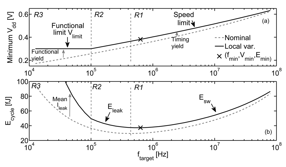
- R1 region where Esw dominates and minimum Vdd is speed limited,
- R2 region where Eleak dominates and minimum Vdd is speed limited,
- R3 region where Eleak dominates and minimum Vdd is limited by functionality.
- A guardband on Tcycle or on the minimum Vdd for sufficient timing (parametric) yield because worst-case delay of critical paths has to be considered given its large statistical distribution;
- Increase in functional limit Vlimit voltage to ensure sufficient functional yield for large chips;
- Increase in mean leakage Ileak because Ileak is a lognormal distribution (exponentially dependent on the normally-distributed Vt) with a mean value higher than the typical one.
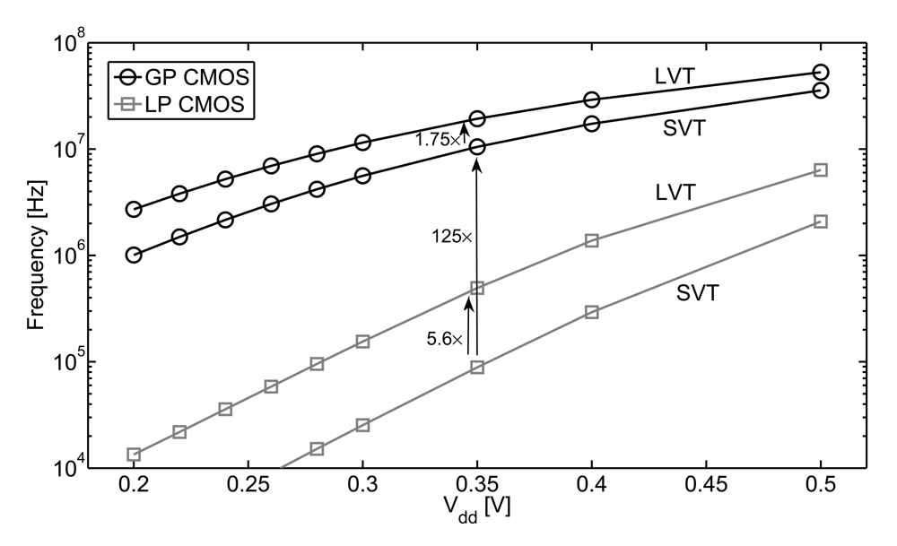
3. Speed Limit on Vdd
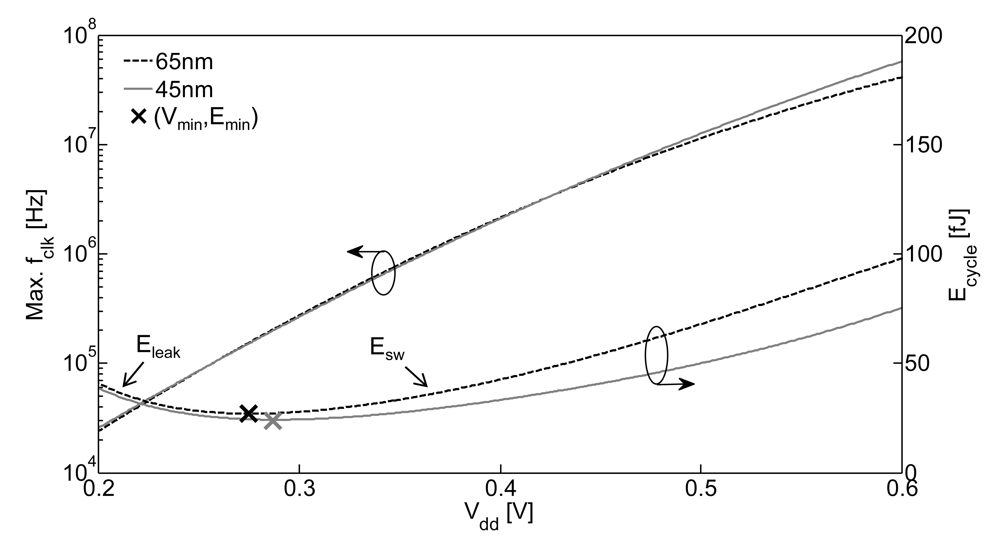
3.1. Timing Constraint and the Minimum-Energy Point
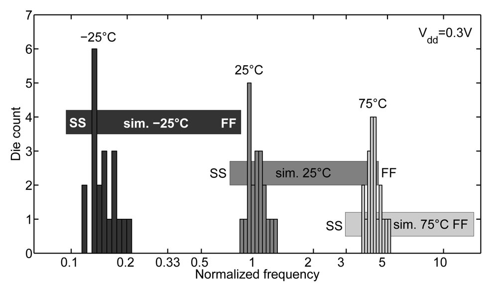
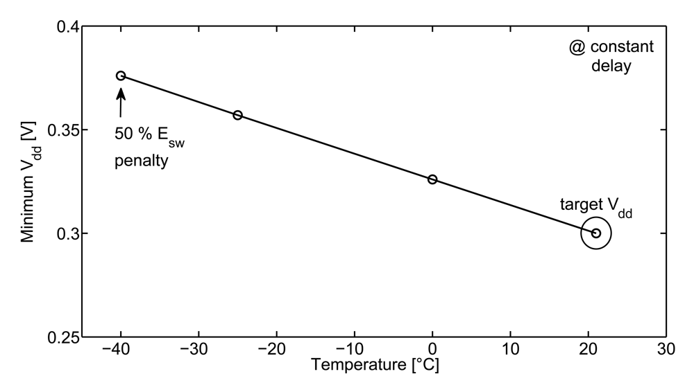
3.2. Timing Constraint and Process/Temperature Variations
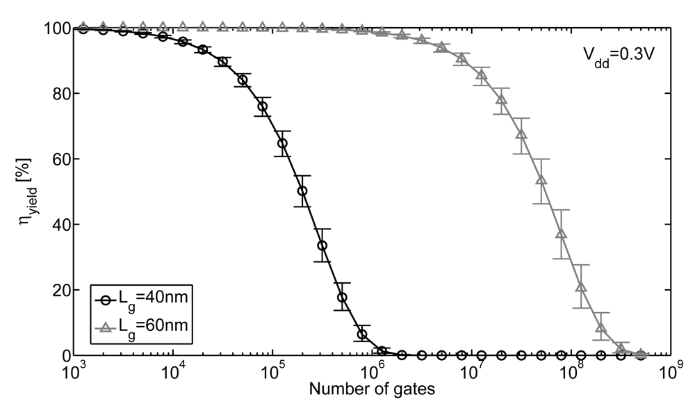
4. Functional Limits on Vdd
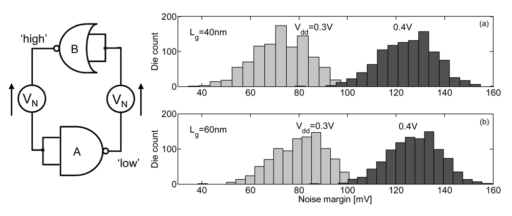
4.1. Noise Margin Constraint
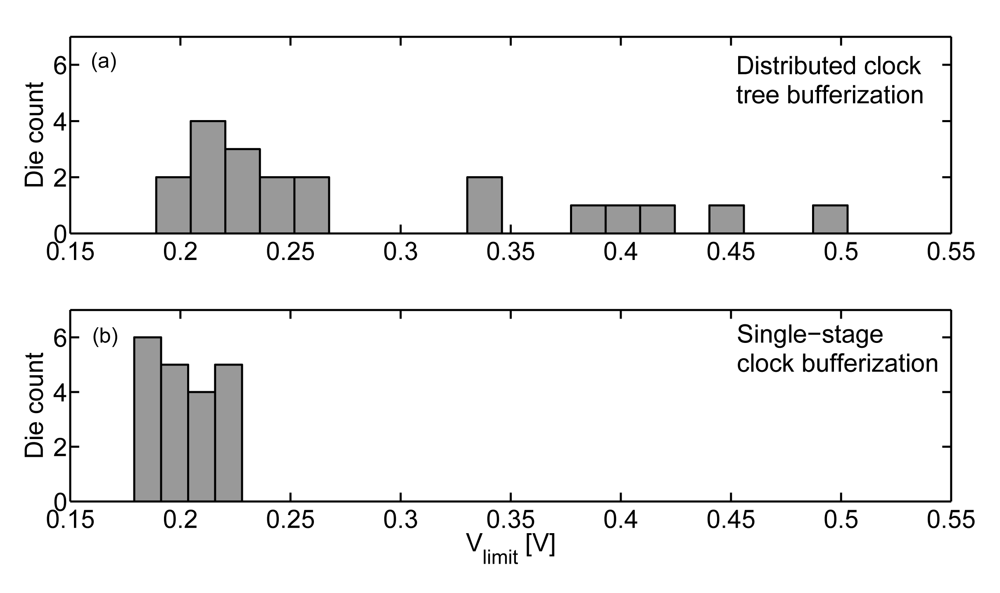
4.2. Hold Time Constraint
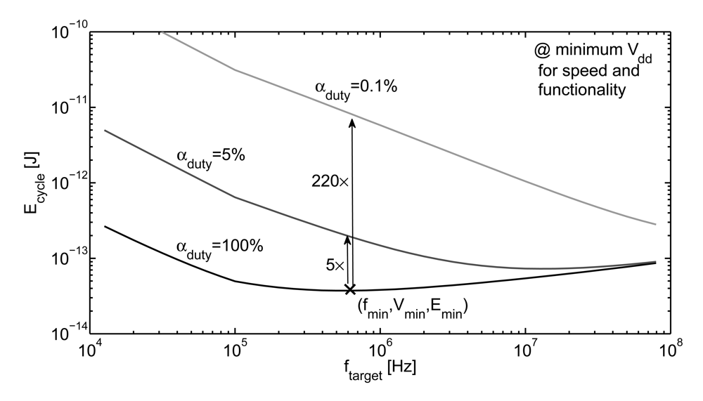
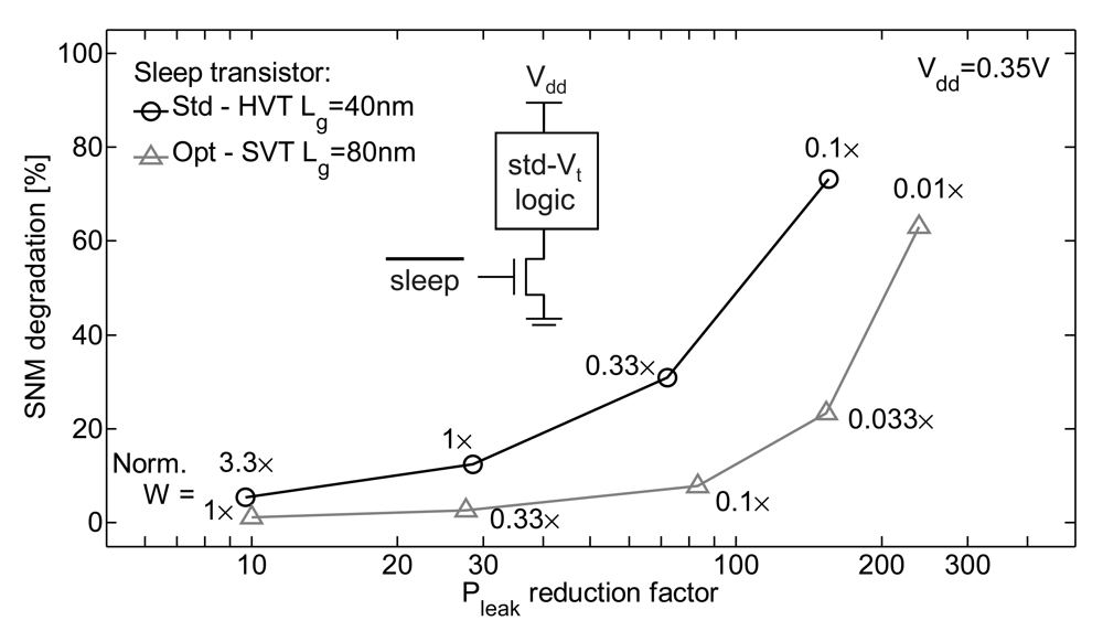
5. Energy Efficiency and Stand-By Periods
6. Conclusions


| Challenge | Circuit consequence | Preferred solution |
|---|---|---|
| Mismatch between ftarget and fmin | Ecycle penalty | Process flavor & Vt selection |
| Operation at −40 °C | Delay increase—Tcycle guardband | Adaptive voltage scaling |
| Degraded noise margins | Soft and hard errors—Vlimit increase | Upsized Lg & logic gate restriction |
| Variability-induced clock skew | Hold time violations—Vlimit increase | Single-stage clock bufferization |
| Long stand-by periods | Effective Ecycle penalty | Power gating with opt. sleep transistor |
Acknowledgments
References
- Bianchini, R.; Rajamony, R. Power and energy management for server systems. Computer 2004, 37, 68–76. [Google Scholar]
- Gammie, G.; Wang, A.; Mair, H.; Lagerquist, R.; Chau, M.; Royannez, P.; Gururajarao, S.; Ko, U. SmartReflex Power and Performance Management Technologies for 90 nm, 65 nm, and 45 nm Mobile Application Processors. Proc. IEEE 2010, 98, 144–159. [Google Scholar]
- Wang, A.; Calhoun, B.; Chandrakasan, A. Sub-Threshold Design for Ultra-Low-Power Systems; Springer: New York, NY, USA, 2006. [Google Scholar]
- Warneke, B.; Pister, K. An ultra-low energy microcontroller for Smart Dust wireless sensor networks. Proceedings of the 2004 IEEE International Solid-State Circuits Conference, San Francisco, CA, USA; 2004; pp. 316–317. [Google Scholar]
- Chen, G.; Fojtik, M.; Kim, D.; Fick, D.; Park, J.; Seok, M.; Chen, M.T.; Foo, Z.; Sylvester, D.; Blaauw, D. Millimeter-scale nearly perpetual sensor system with stacked battery and solar cells. Proceedings of the 2010 IEEE International Solid-State Circuits Conference, San Francisco, CA, USA; 2010; pp. 288–289. [Google Scholar]
- Bol, D.; Ambroise, R.; Flandre, D.; Legat, J.D. Analysis and minimization of practical energy in 45nm subthreshold logic circuits. Proceedings of the 2008 IEEE International Conference on Computer Design, Lake Tahoe, CA, USA; 2008; pp. 294–300. [Google Scholar]
- Swanson, R.; Meindl, J. Ion-implanted complementary MOS transistors in low-voltage circuits. IEEE J. Solid-State Circuits 1972, 7, 146–153. [Google Scholar]
- Vittoz, E.; Fellrath, J. CMOS analog integrated circuits based on weak inversion operations. IEEE J. Solid-State Circuits 1977, 12, 224–231. [Google Scholar]
- Soeleman, H.; Roy, K. Ultra-low power digital subthreshold logic circuits. Proceedings of the 1999 ACM/IEEE International Symposium on Low Power Electronics and Design, San Diego, CA, USA; 1999; pp. 94–96. [Google Scholar]
- Kao, J.; Miyazaki, M.; Chandrakasan, A. A 175-mV multiply-accumulate unit using an adaptive supply voltage and body bias architecture. IEEE J. Solid-State Circuits 2002, 37, 1545–1554. [Google Scholar]
- Calhoun, B.; Wang, A.; Chandrakasan, A. Modeling and sizing for minimum energy operation in subthreshold circuits. IEEE J. Solid-State Circuit 2005, 40, 1778–1786. [Google Scholar]
- Bol, D.; Ambroise, R.; Flandre, D.; Legat, J.D. Interests and limitations of technology scaling for subthreshold logic. IEEE Trans. VLSI Syst. 2009, 17, 1508–1519. [Google Scholar]
- Kwong, J.; Ramadass, Y.; Verma, N.; Chandrakasan, A. A 65 nm sub-Vt microcontroller with integrated SRAM and switched capacitor DC-DC converter. IEEE J. Solid-State Circuits 2009, 44, 115–126. [Google Scholar]
- Sridhara, S.; DiRenzo, M.; Lingam, S.; Lee, S.J.; Blazquez, R.; Maxey, J.; Ghanem, S.; Lee, Y.H.; Abdallah, R.; Singh, P.; Goe, M. Microwatt embedded processor platform for medical system-on-chip applications. Proceedings of the 2010 IEEE Symposium on VLSI Circuits (VLSIC), Honolulu, HI, USA; 2010; pp. 15–16. [Google Scholar]
- Zhai, B.; Nazhandali, L.; Olson, J.; Reeves, A.; Minuth, M.; Helfand, R.; Pant, S.; Blaauw, D.; Austin, T. A 2.60 pJ/Inst Subthreshold Sensor Processor for Optimal Energy Efficiency. Proceedings of the 2006 IEEE Symposium on VLSI Circuits (VLSIC), Honolulu, HI, USA; 2006. [Google Scholar]
- Kim, C.I.; Soeleman, H.; Roy, K. Ultra-low-power DLMS adaptive filter for hearing aid applications. IEEE Trans. VLSI Syst. 2003, 11, 1058–1067. [Google Scholar]
- Jocke, S.C.; Bolus, J.F.; Wooters, S.N.; Jurik, A.D.; Weaver, A.C.; Blalock, T.N.; Calhoun, B.H. A 2.6-μW sub-threshold mixed-signal ECG SoC. Proceedings of the 2009 IEEE Symposium on VLSI Circuits (VLSIC), Kyoto, Japan; 2009; pp. 60–61. [Google Scholar]
- Sze, V.; Chandrakasan, A. A 0.4-V UWB baseband processor. Proceedings of the 2007 ACM/IEEE International Symposium on Low Power Electronics and Design, Portland, OR, USA; 2007; pp. 262–267. [Google Scholar]
- Sze, V.; Finchelstein, D.; Sinangil, M.; Chandrakasan, A. A 0.7-V 1.8-mWH.264/AVC 720p Video Decoder. IEEE J. Solid-State Circuits 2009, 44, 2943–2956. [Google Scholar]
- Pu, Y.; Pineda de Gyvez, J.; Corporaal, H.; Ha, Y. An Ultra-Low-Energy Multi-Standard JPEG Co-Processor in 65 nm CMOS With Sub/Near Threshold Supply Voltage. IEEE J. Solid-State Circuits 2010, 45, 668–680. [Google Scholar]
- Hocquet, C.; Kamel, D.; Regazzoni, F.; Legat, J.D.; Flandre, D.; Bol, D.; Standaert, F.-X. Harvesting the potential of nano-CMOS for lightweight cryptography: An ultra-low-voltage 65 nm AES coprocessor for passive RFID tags. J. Cryptogr. Eng. 2011, 1, 8. [Google Scholar]
- Bol, D.; Flandre, D.; Legat, J.D. Technology flavor selection and adaptive techniques for timing-constrained 45 nm subthreshold circuits. Proceedings of the 2009 ACM/IEEE International Symposium on Low Power Electronics and Design, San Francisco, CA, USA; 2009; pp. 21–26. [Google Scholar]
- Bol, D.; Kamel, D.; Flandre, D.; Legat, J.D. Nanometer MOSFET effects on the minimum-energy point of 45 nm subthreshold logic. Proceedings of the 2009 ACM/IEEE International Symposium on Low Power Electronics and Design, San Francisco, CA, USA; 2009; pp. 3–8. [Google Scholar]
- Bol, D.; Hocquet, C.; Flandre, D.; Legat, J.D. Robustness-aware sleep transistor engineering for power-gated nanometer subthreshold circuits. Proceedings of the 2010 IEEE International Symposium on Circuits and System, Paris, France; 2010; pp. 1484–1487. [Google Scholar]
- Bol, D.; Hocquet, C.; Flandre, D.; Legat, J.D. The detrimental impact of negative Celsius temperature on ultra-low-voltage CMOS logic. Proceedings of the 2010 European Solid-State Circuit Research Conference, Seville, Spain; 2010; pp. 522–525. [Google Scholar]
- Dennard, R.; Gaensslen, F.; Rideout, V.; Bassous, E.; LeBlanc, A. Design of ion-implanted MOSFET's with very small physical dimensions. IEEE J. Solid-State Circuits 1974, 9, 256–268. [Google Scholar]
- Roy, K.; Mukhopadhyay, S.; Mahmoodi-Meimand, H. Leakage current mechanisms and leakage reduction techniques in deep-submicrometer CMOS circuits. Proc. IEEE 2003, 91, 305–327. [Google Scholar]
- Asenov, A.; Brown, A.; Davies, J.; Kaya, S.; Slavcheva, G. Simulation of intrinsic parameter fluctuations in decananometer and nanometer-scale MOSFETs. IEEE Trans. Electron Device 2003, 50, 1837–1852. [Google Scholar]
- Bol, D.; Flandre, D.; Legat, J.D. Nanometer MOSFET Effects on the Minimum-Energy Point of Sub-45 nm Subthreshold Logic—Mitigation at Technology and Circuit Levelsc. ACM Trans. Design Autom. Electr. Syst. 2010, 16, 2–26. [Google Scholar]
- Seok, M.; Sylvester, D.; Blaauw, D. Optimal technology selection for minimizing energy and variability in low voltage applications. Proceedings of the 2008 ACM/IEEE International Symposium on Low Power Electronics and Design, Bangalore, India; 2008; pp. 9–14. [Google Scholar]
- Zhai, B.; Hanson, S.; Blaauw, D.; Sylvester, D. Analysis and mitigation of variability in subthreshold design. Proceedings of the 2005 ACM/IEEE International Symposium on Low Power Electronics and Design, San Diego, CA, USA; 2005; pp. 20–25. [Google Scholar]
- Kamel, D.; Hocquet, C.; Standaert, F.X.; Flandre, D.; Bol, D. Glitch-induced within-die variations of dynamic energy in voltage-scaled nano-CMOS circuits. Proceedings of the 2010 European Solid-State Circuit Research Conference, Seville, Spain; 2010; pp. 518–521. [Google Scholar]
- Kwong, J.; Chandrakasan, A. Variation-Driven Device Sizing for Minimum Energy Sub-threshold Circuits. Proceedings of the 2006 ACM/IEEE International Symposium on Low Power Electronics and Design, Tegernsee, Germany; 2006; pp. 8–13. [Google Scholar]
- Alioto, M. Understanding DC Behavior of Subthreshold CMOS Logic Through Closed-Form Analysis. IEEE Trans. Circuits Syst. I 2010, 57, 1597–1607. [Google Scholar]
- Nanua, M.; Blaauw, D. Investigating Crosstalk in Sub-Threshold Circuits. Proceedings of the 8th International Symposium on Quality Electronic Design, San Jose, CA, USA; 2007; pp. 639–646. [Google Scholar]
- Dhillon, Y.; Diril, A.; Chatterjee, A.; Singh, A. Analysis and optimization of nanometer CMOS circuits for soft-error tolerance. IEEE Trans. VLSI Syst. 2006, 14, 514–524. [Google Scholar]
- Verma, N.; Kwong, J.; Chandrakasan, A. Nanometer MOSFET variation in minimum energy subthreshold circuits. IEEE Trans. Electron Device 2008, 55, 163–174. [Google Scholar]
- Niiyama, T.; Piao, Z.; Ishida, K.; Murakata, M.; Takamiya, M.; Sakurai, T. Increasing minimum operating voltage (VDDmin) with number of CMOS logic gates and experimental verification with up to 1 Mega-stage ring oscillators. Proceedings of the 2008 ACM/IEEE International Symposium on Low Power Electronics and Design, Bangalore, India; 2008; pp. 117–122. [Google Scholar]
- Pu, Y.; de Gyvez, J.; Corporaal, H.; Ha, Y. Statistical noise margin estimation for sub-threshold combinational circuits. Proceedings of the 13th Asia and South Pacific Design Automation Conference, Seoul, Korea; 2008; pp. 176–179. [Google Scholar]
- Pu, Y.; de Jesus Pineda de Gyvez, J.; Corporaal, H.; Ha, Y. Vt balancing and device sizing towards high yield of sub-threshold static logic gates. Proceedings of the 2007 ACM/IEEE International Symposium on Low Power Electronics and Design, Portland, OR, USA; 2007; pp. 355–358. [Google Scholar]
- Hwang, M.E.; Roy, K. ABRM: Adaptive β-Ratio Modulation for Process-Tolerant Ultradynamic Voltage Scaling. IEEE Trans. VLSI Syst. 2010, 18, 281–290. [Google Scholar]
- Seok, M.; Blaauw, D.; Sylvester, D. Clock network design for ultra-low power applications. Proceedings of the 2010 ACM/IEEE International Symposium on Low Power Electronics and Design, Austin, DX, USA; 2010; pp. 271–276. [Google Scholar]
- Hanson, S.; Zhai, B.; Seok, M.; Cline, B.; Zhou, K.; Singhal, M.; Minuth, M.; Olson, J.; Nazhandali, L.; Austin, T.; Sylvester, D.; Blaauw, D. Exploring Variability and Performance in a Sub-200-mV Processor. IEEE J. Solid-State Circuits 2008, 43, 881–891. [Google Scholar]
- Hanson, S.; Seok, M.; Lin, Y.S.; Foo, Z.Y.; Kim, D.; Lee, Y.; Liu, N.; Sylvester, D.; Blaauw, D. A Low-Voltage Processor for Sensing Applications With Picowatt Standby Mode. IEEE J. Solid-State Circuits 2009, 44, 1145–1155. [Google Scholar]
- Seok, M.; Hanson, S.; Sylvester, D.; Blauw, D. Analysis and optimization of sleep modes in subthreshold circuit design. Proceedings of the 44th ACM/IEEE Design Automation Conference, San Diego, CA, USA; 2007; pp. 604–699. [Google Scholar]
- Khanna, S.; Calhoun, B.H. Serial sub-threshold circuits for ultra-low-power systems. Proceedings of the 14th ACM/IEEE International Symposium on Low Power Electronics and Design, New York, NY, USA; 2009; pp. 27–32. [Google Scholar]
© 2011 by the author; licensee MDPI, Basel, Switzerland. This article is an open access article distributed under the terms and conditions of the Creative Commons Attribution license (http://creativecommons.org/licenses/by/3.0/.)
Share and Cite
Bol, D. Robust and Energy-Efficient Ultra-Low-Voltage Circuit Design under Timing Constraints in 65/45 nm CMOS. J. Low Power Electron. Appl. 2011, 1, 1-19. https://doi.org/10.3390/jlpea1010001
Bol D. Robust and Energy-Efficient Ultra-Low-Voltage Circuit Design under Timing Constraints in 65/45 nm CMOS. Journal of Low Power Electronics and Applications. 2011; 1(1):1-19. https://doi.org/10.3390/jlpea1010001
Chicago/Turabian StyleBol, David. 2011. "Robust and Energy-Efficient Ultra-Low-Voltage Circuit Design under Timing Constraints in 65/45 nm CMOS" Journal of Low Power Electronics and Applications 1, no. 1: 1-19. https://doi.org/10.3390/jlpea1010001