Rotating Circular Micro-Platform with Integrated Waveguides and Latching Arm for Reconfigurable Integrated Optics

 and
and
Abstract
:1. Introduction
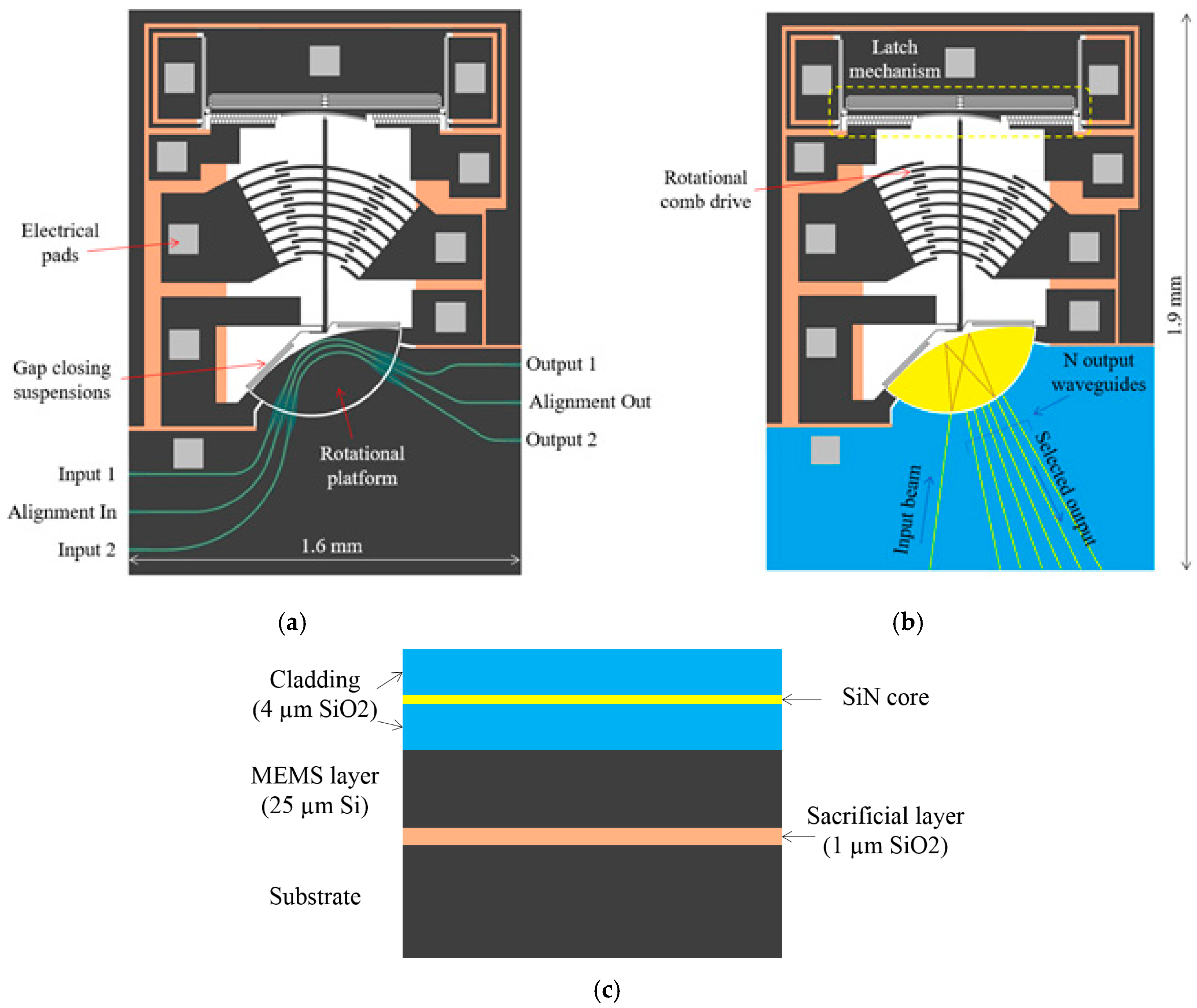
2. System Overview
2.1. Targeted Micro-Opto-Electro-Mechanical System
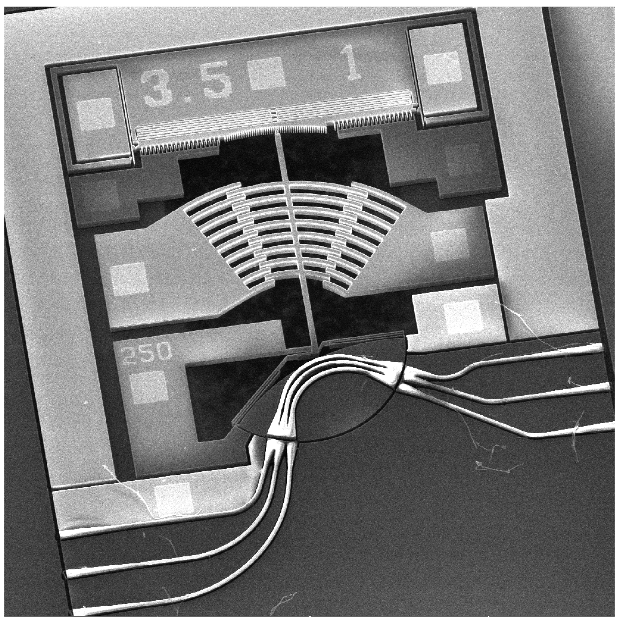
2.2. Micro-Platform
3. Device Designs
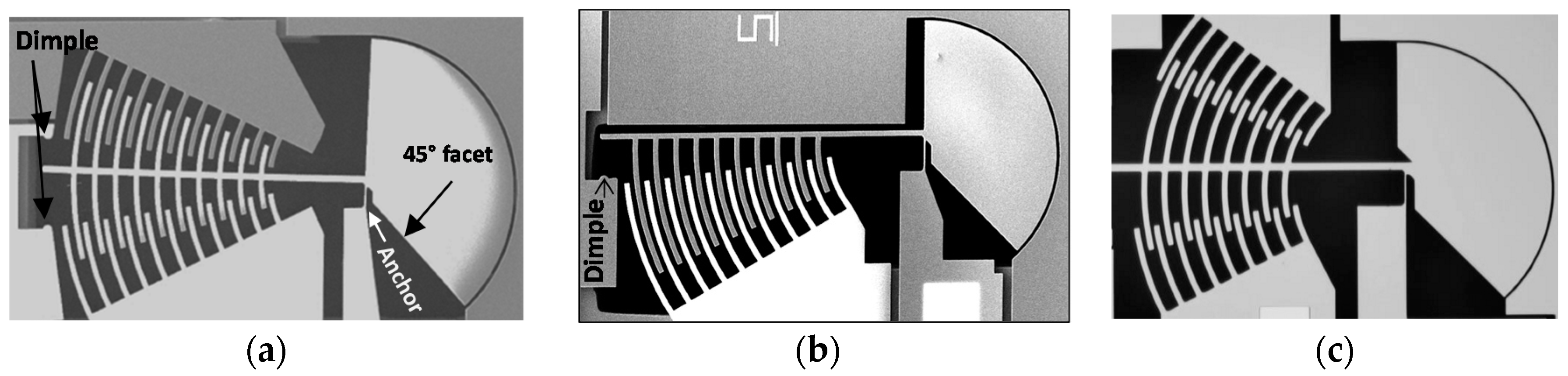
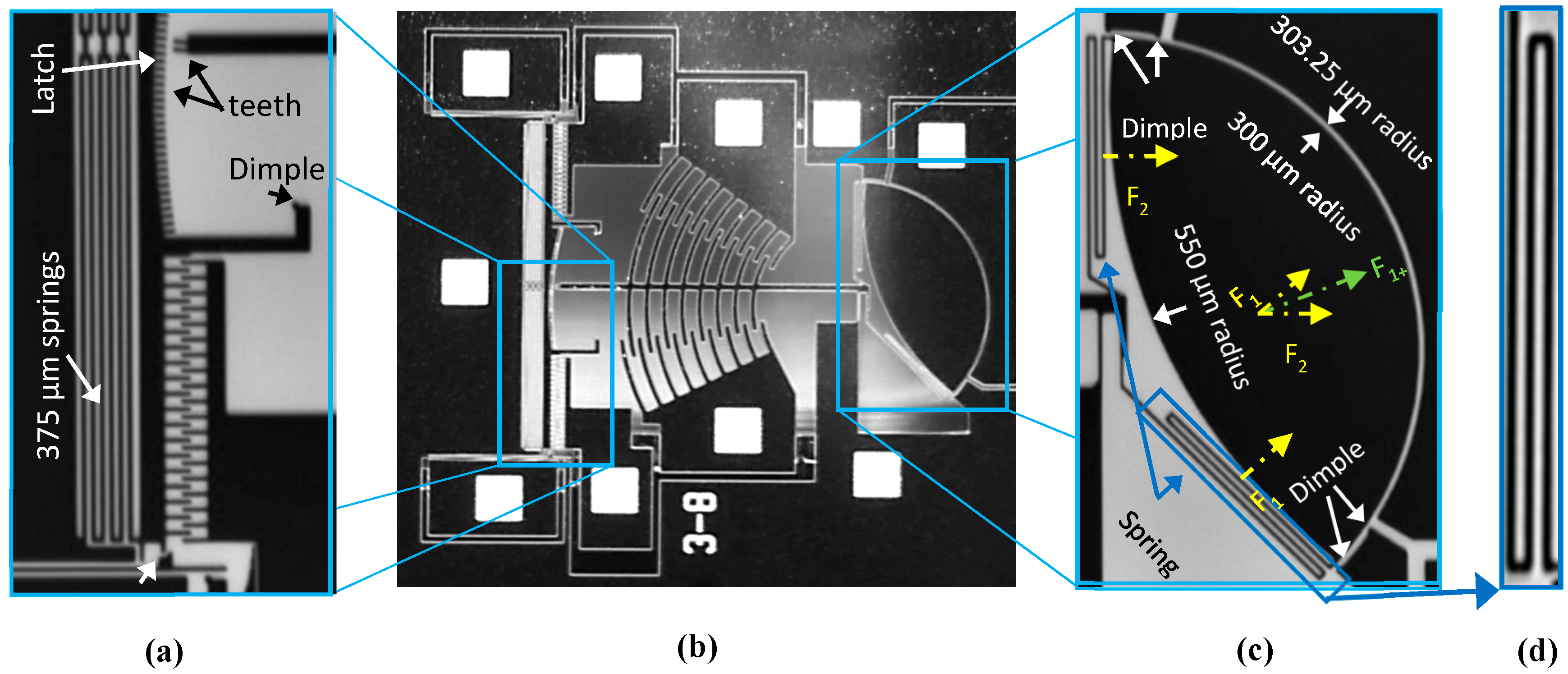
3.1. Rotational Actuators
3.2. Latch and Latch Lock
3.3. Gap Closer
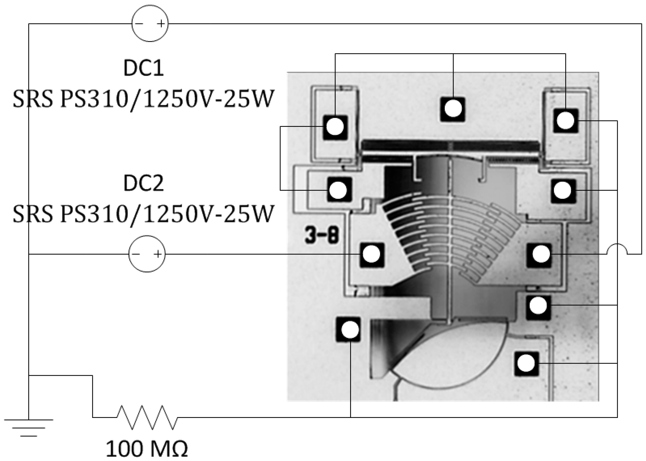
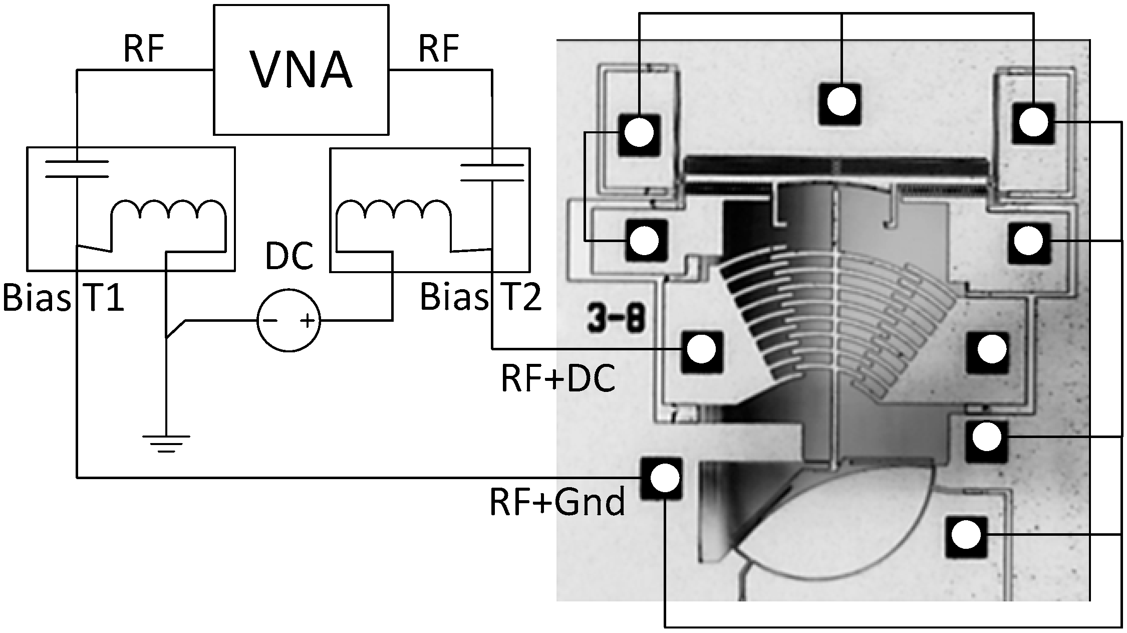
4. Test Setups
5. Results
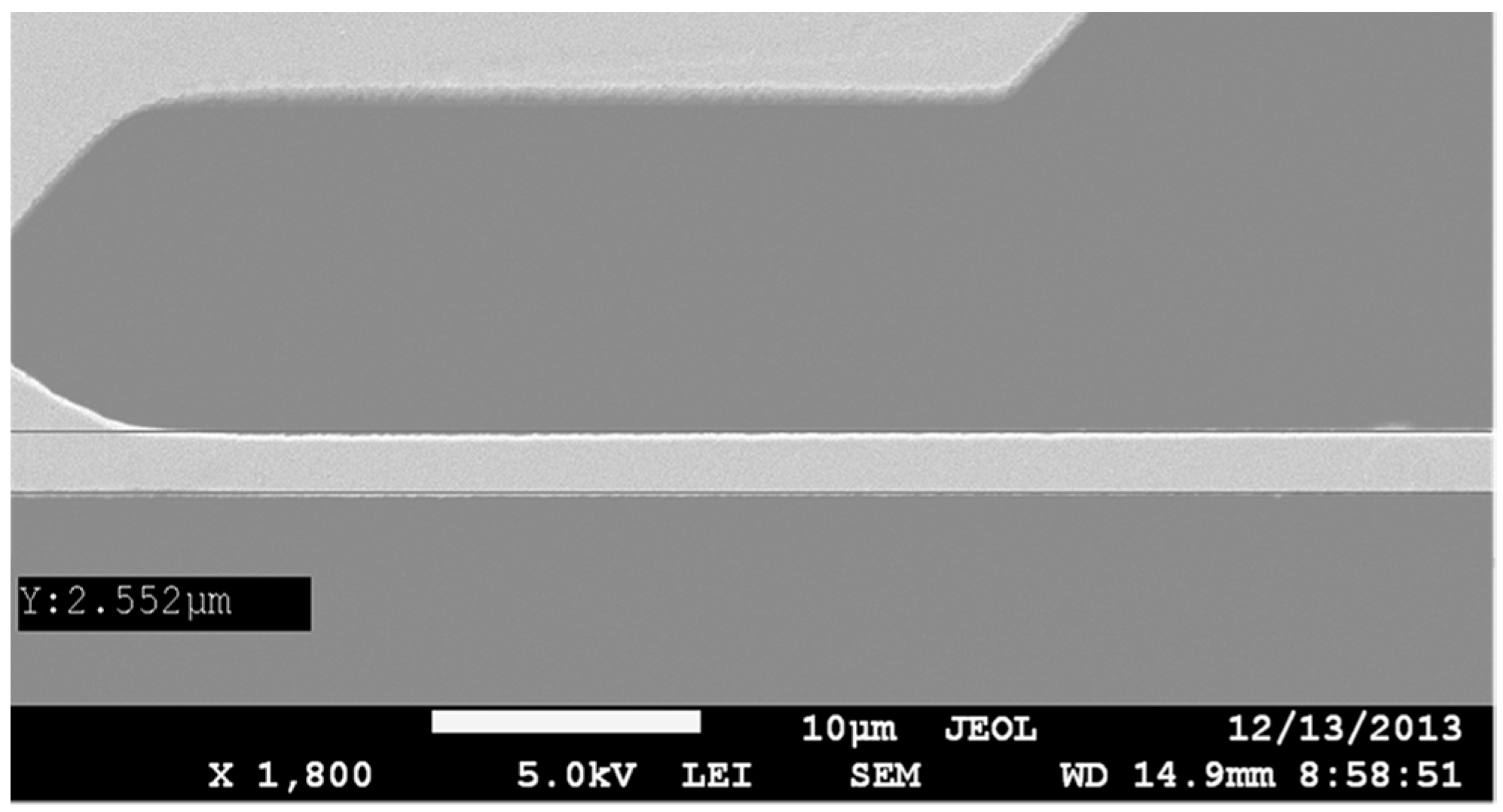
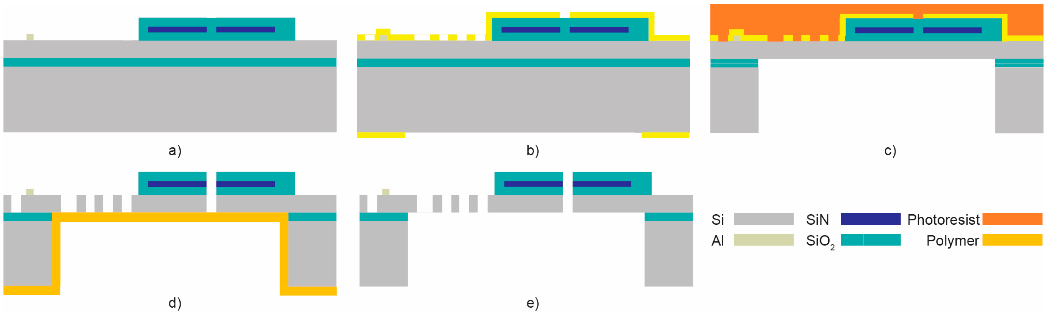
5.1. Fabrication Process Characterization
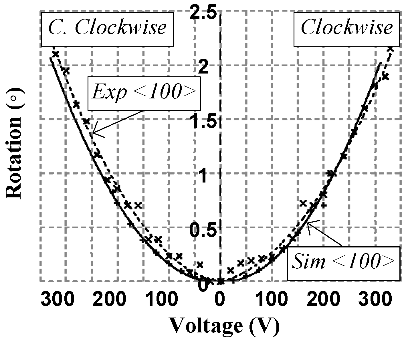
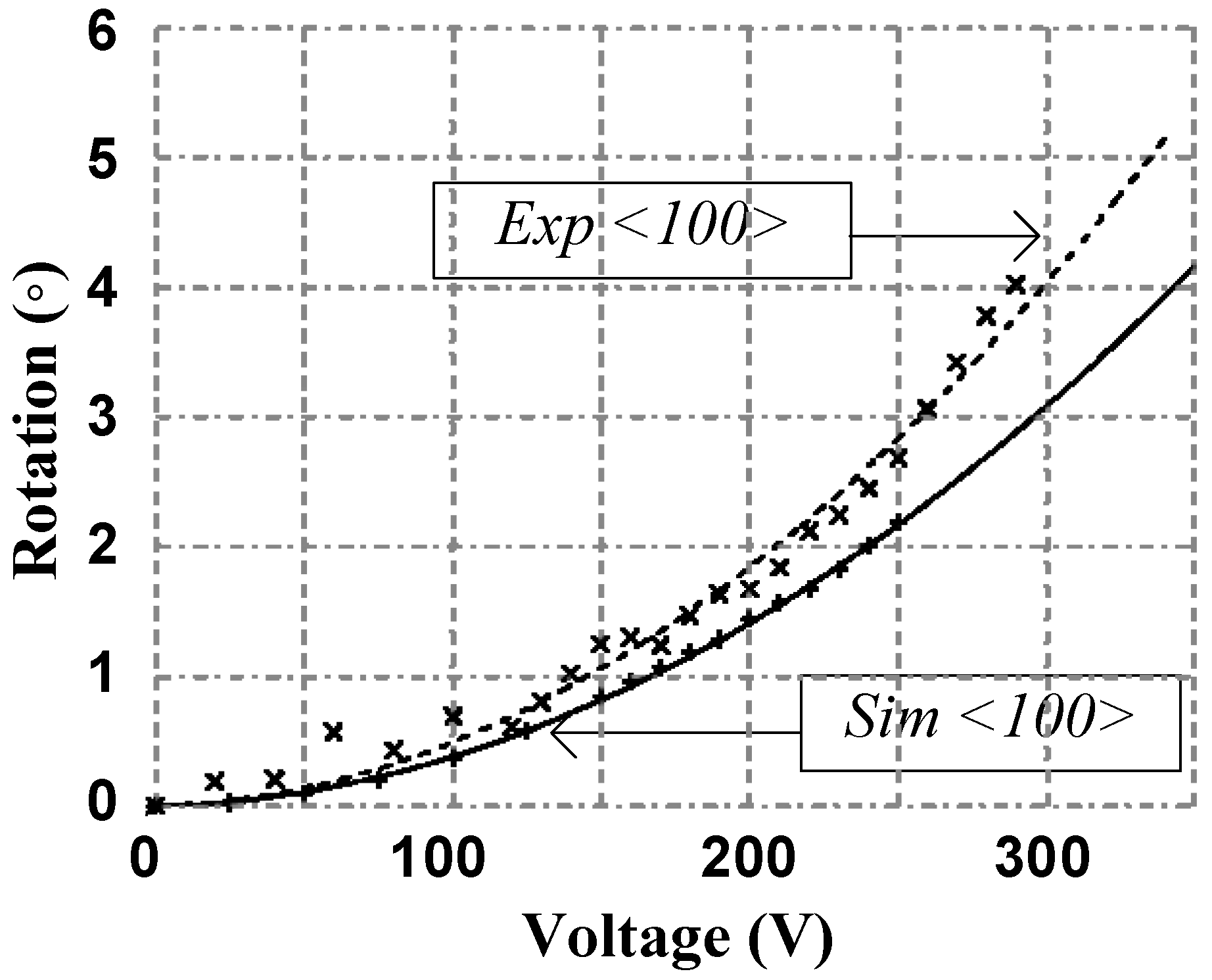
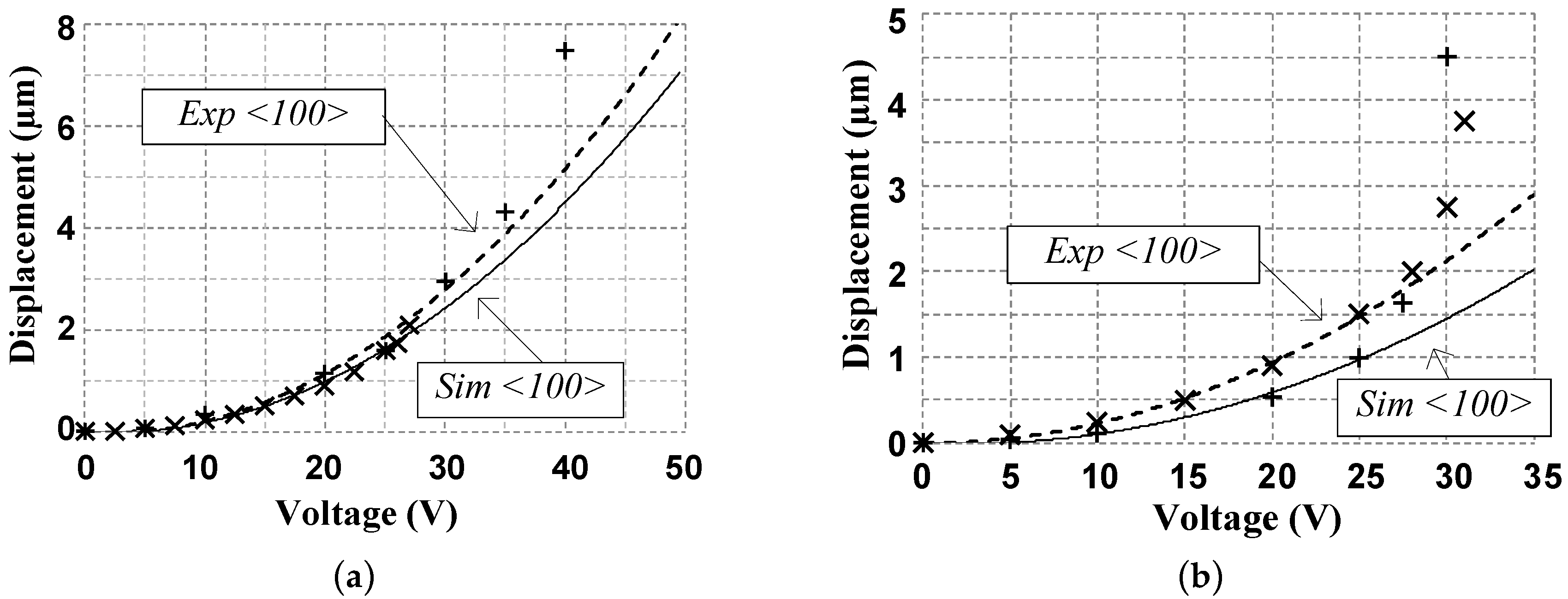
5.2. First Design
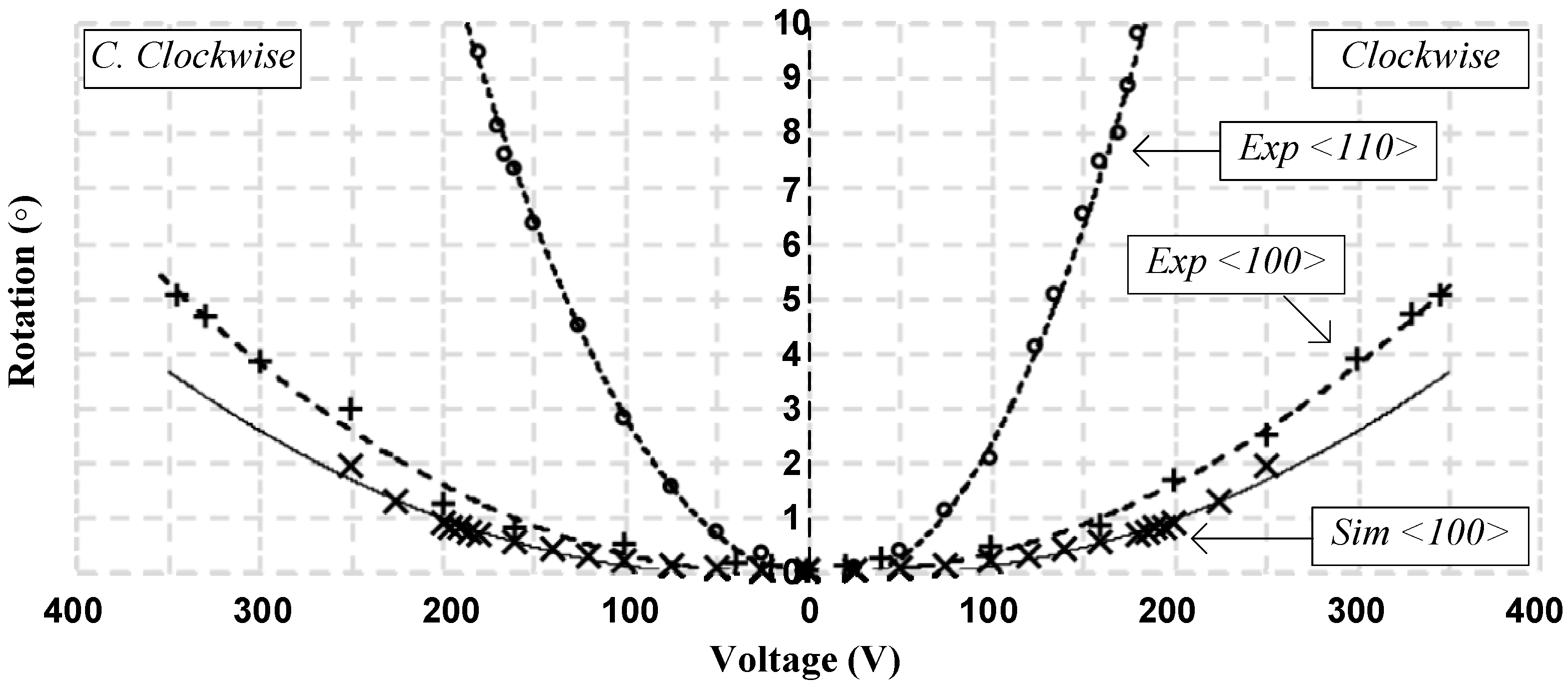
5.3. Second Design
5.4. Third Design
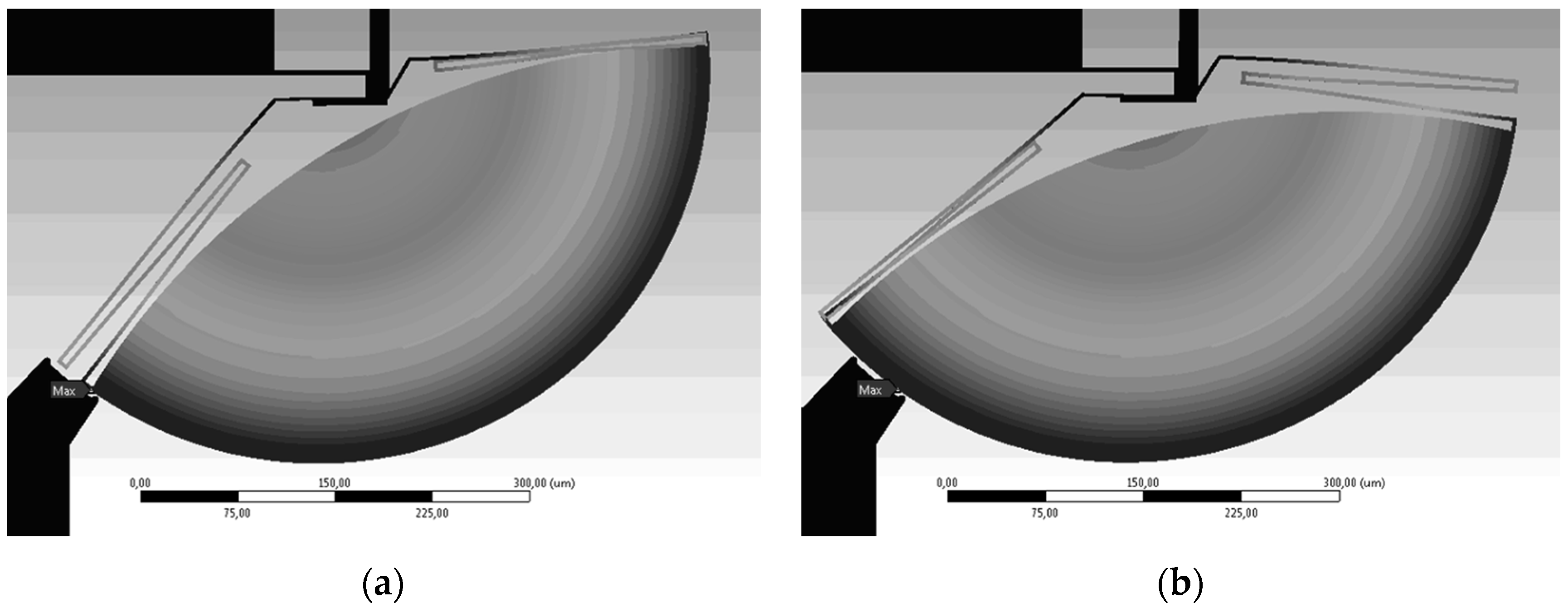
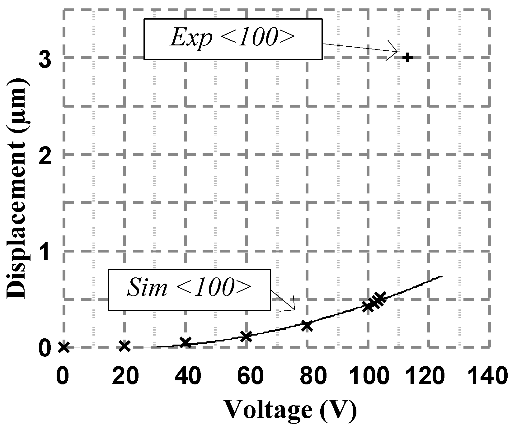
5.5. Latch and Gap Closer
5.6. Optical Measurements of a Crossbar Switch Cell
6. Discussion
7. Conclusions
Acknowledgments
Author Contributions
Conflicts of Interest
References
- Wu, M. Micromachining for Optical and Optoelectronic Systems. Proc. IEEE 1997, 85, 1833–1856. [Google Scholar] [CrossRef]
- Li, G.; Yao, J.; Thacker, H.; Mekis, A.; Zheng, X.; Shubin, I.; Luo, Y.; Lee, J.; Raj, K.; Cunningham, J.E.; et al. Ultralow-loss, high-density SOI optical waveguide routing for macrochip interconnects. Opt. Express 2012, 20, 12035–12039. [Google Scholar] [CrossRef] [PubMed]
- Bogaerts, W.; Selvaraja, S.K.; Dumon, P.; Brouckaert, J.; de Vos, K.; van Thourhout, D.; Baets, R. Silicon-on-insulator spectral filters fabricated with CMOS technology. IEEE J. Sel. Topics Quantum Electron. 2010, 16, 33–44. [Google Scholar] [CrossRef]
- Ford, J. Optical MEMS: Legacy of the telecom boom. In Proceedings of the Solid-State Sensors, Actuators Microsystems Workshop, Hilton Head Island, SC, USA, 6–10 June 2004; pp. 1–3. [Google Scholar]
- Rahim, M.; Akkary, P.; Jamaleddine, N.; Nabki, F.; Menard, M. An integrated silicon-on-insulator continually tunable optical delay line for optical coherence tomography. In Proceedings of the 2013 IEEE 56th International Midwest Symposium on Circuits and Systems (MWSCAS), Columbus, OH, USA, 4–7 August 2013; pp. 709–712. [Google Scholar]
- Klein, E.J.; Geuzebroek, D.H.; Kelderman, H.; Sengo, G.; Baker, N.; Driessen, A. Reconfigurable optical add-drop multiplexer using microring resonators. IEEE Photonics Technol. Lett. 2005, 17, 2358–2360. [Google Scholar] [CrossRef]
- Boysel, R.M.; McDonald, T.G.; Magel, G.A.; Smith, G.C.; Leonard, J.L. Integration of deformable mirror devices with optical fibers and waveguides. Proc. SPIE 1993, 1793, 34–39. [Google Scholar]
- Lin, P.-Y.; Hsieh, H.-T.; Su, G.-D.J. Design and fabrication of a large-stroke MEMS deformable mirror for wavefront control. J. Opt. 2011, 13, 055404. [Google Scholar] [CrossRef]
- Ikeda, M.; Goto, H.; Sakata, M.; Wakabayashi, S.; Imanaka, K.; Takeuchi, M.; Yada, T. Two dimensional silicon micromachined optical scanner integrated with photo detector. Proc. SPIE 1995, 2383, 118. [Google Scholar]
- Miller, R.; Burr, G.; Tai, Y.; Psaltis, D. Electromagnetic MEMS scanning mirrors for holographic data storage. In Proceedings of the Solid-State Sensors, Actuators Microsystems Workshop, Hilton Head Island, SC, USA, 1996; pp. 183–186. [Google Scholar]
- Seok, T.J.; Quack, N.; Han, S.; Muller, R.S.; Wu, M.C. Large-scale broadband digital silicon photonic switches with vertical adiabatic couplers. Optica 2016, 3, 64–70. [Google Scholar] [CrossRef]
- Han, S.; Seok, T.J.; Quack, N.; Yoo, B.; Wu, M.C. Large-scale silicon photonic switches with movable directional couplers. Optica 2014, 2, 370–375. [Google Scholar] [CrossRef]
- Akihama, Y.; Hane, K. Single and multiple optical switches that use freestanding silicon nanowire waveguide couplers. Light Sci. Appl. 2012, 1, e16. [Google Scholar] [CrossRef]
- Toshiyoshi, H.; Fujita, H. An electrostatically operated torsion mirror for optical switching devices. In Proceedings of the 8th International Conference on Solid-State Sensors and Actuators, Stockholm, Sweden, 25–29 June 1995; pp. 297–300. [Google Scholar]
- Petersen, K. Silicon torsional scanning mirror. IBM J. Res. Dev. 1980, 24, 631–637. [Google Scholar] [CrossRef]
- Du, H.; Chao, F.; Zhou, G. Mechanically-tunable photonic devices with on-chip integrated MEMS/NEMS actuators. Micromachines 2016, 7, 69. [Google Scholar] [CrossRef]
- Chollet, F. Devices based on co-integrated MEMS actuators and optical waveguide: A review. Micromachines 2016, 7, 18. [Google Scholar] [CrossRef]
- Liu, Y.; Xu, J.; Zhong, S.; Wu, Y. Large size MEMS scanning mirror with vertical comb drive for tunable optical filter. Opt. Lasers Eng. 2013, 51, 54–60. [Google Scholar] [CrossRef]
- Yeh, J.A.; Chen, C.N.; Lui, Y.S. Large rotation actuated by in-plane rotary comb-drives with serpentine spring suspension. J. Micromech. Microeng. 2005, 15, 201–206. [Google Scholar] [CrossRef]
- Yeh, J.A.; Huang, J.Y.; Chen, C.N.; Hui, C.Y. Design of an electrostatic rotary comb actuator. J. Micro/Nanolith. MEMS MOEMS 2006, 5, 023008. [Google Scholar]
- Yeh, J.; Jiang, S.S.; Lee, C. MOEMS variable optical attenuators using rotary comb drive actuators. IEEE Photonic Technol. Lett. 2006, 18, 1170–1172. [Google Scholar] [CrossRef]
- Hou, M.; Huang, J.-Y.; Jiang, S.-S.; Yeh, J. In-plane rotary comb-drive actuator for a variable optical attenuator. J. Micro/Nanolith. MEMS MOEMS 2008, 7, 043015. [Google Scholar]
- Zhang, X.M.; Liu, A.Q.; Lu, C.; Tang, D.Y. A real pivot structure for MEMS tunable lasers. J. Microelectromech. Syst. 2007, 16, 269–278. [Google Scholar] [CrossRef]
- Huda, M.Q.; Amin, T.M.F.; Ning, Y.; McKinnon, G.; Tulip, J.; Jäger, W. Rotary MEMS comb-drive actuator with large deflection for photonic applications. Proc. SPIE 2012, 8248, 824804. [Google Scholar]
- Amin, T.M.F.; Huda, M.Q.; Ning, Y.; McKinnon, G.; Tulip, J.; Jäger, W. A virtual pivot point MEMS rotary comb actuator for tunable laser applications. Proc. SPIE 2012, 8490, 84900D. [Google Scholar]
- Amin, T.; Huda, M.; Tulip, J.; Jäger, W. Design and fabrication of a long arm comb drive rotary actuator with externally mounted mirror for optical applications. J. Mecoelectromech. Syst. 2015, 24, 1565–1574. [Google Scholar] [CrossRef]
- Ilkhechi, A.; Mirzajani, H.; Aghdam, E.; Ghaviferk, H. A new electrostatically actuated rotary three-state DC-contact RF MEMS switch for antenna switch applications. Microsyst. Technol. 2015. [Google Scholar]
- Chang, H.; Zhao, H.; Ye, F.; Yuan, G.; Xie, J.; Kraft, M.; Yuan, W. A rotary comb-actuated microgripper with a large displacement range. Microsyst. Technol. 2014, 20, 119–126. [Google Scholar] [CrossRef]
- Briere, J.; Beaulieu, P.-O.; Saidani, M.; Nabki, F.; Menard, M. Rotational MEMS mirror with latching arm for silicon photonics. Proc. SPIE 2015, 9375, 937507. [Google Scholar]
- Menard, M.; Nabki, F.; Rahim, M.; Briere, J.; Beaulieu, P.-O. Mirror Based Microelectromechanical Systems and Methods. International Patent Application PCT/CA2015/000136, WO 2015/131271 A1, March 2015. [Google Scholar]
- De Ridder, R.M.; Warhoff, K.; Driessen, A.; Lambeck, P.V.; Albers, H. Silicon Oxynitride Planar Waveguiding Structures for Application in Optical Communication. IEEE J. Sel. Top. Quantum Electron. 1998, 4, 930–937. [Google Scholar] [CrossRef]
- Heideman, R.; Leinse, A.; Hoving, W.; Dekker, R.; Geuzebroek, D.; Klein, E.; Stoffer, R.; Roeloffzen, C.; Zhuang, L.; Meijerink, A. Large-scale integrated optics using TriPleXTM waveguide technology: From UV to IR. Proc. SPIE 2009, 7221, 72210R. [Google Scholar]
- Tabti, B.; Nabki, F.; Ménard, M. Polarization insensitive sampled Bragg gratings. In Proceedings of the Photonics North, Ottawa, ON, Canada, 6–8 June 2017. [Google Scholar]
- Tabti, B.; Nabki, F.; Ménard, M. Polarization insensitive Bragg gratings in silicon nitride waveguides. In Proceedings of the Integrated Photonics Research, Silicon, and NanoPhotonics, New Orleans, LA, USA, 24–27 July 2017. [Google Scholar]
- Chi, C.-H.; Tsai, J.C.; Hah, D.; Jeong, K.-H.; Wu, M.C. Solid-immersion micromirror with enhanced angular deflection for silicon-based planar lightwave circuits. In Proceedings of the IEEE/LEOS International Conference on Optical MEMS and Their Applications, Oulu, Finland, 1–4 August 2005; pp. 131–132. [Google Scholar]
- Ménard, M.; Elsayed, M.Y.; Brière, J.; Rabbani-Haghighi, H.; Saidani, M.; Bérard, M.; Ménard, F.; Nabki, F. Integrated optical switch controlled with a MEMS rotational electrostatic actuator. In Proceedings of the Photonics in Switching, New Orleans, LA, USA, 24–27 July 2017. [Google Scholar]
- Beaulieu, P.-O.; Alameh, A.H.; Menard, M.; Nabki, F. A 360 V high voltage reconfigurable charge pump in 0.8 μm CMOS for optical MEMS applications. In Proceedings of the 2016 IEEE International Symposium on Circuits and Systems (ISCAS), Montreal, QC, Canada, 22–25 May 2016; pp. 1630–1633. [Google Scholar]
- Cowen, A.; Hames, G.; Monk, D.; Wilcenski, S.; Hardy, B. SOIMUMPs Design Handbook; rev. 8.0; MEMSCAP Inc.: Bernin, France, 2011. [Google Scholar]
- Kim, J.; Cho, D.-I.; Muller, R.S. Why is (111) silicon a better mechanical material for mems? In Proceedings of the International Conference on Solid-State Sensors and Actuators, Munich, Germany, 10–14 June 2001; Transducers ’01 Eurosensors XV. pp. 662–665. [Google Scholar]
- Hopcroft, M.; Nix, W.; Kenny, T. What is the Young’s modulus of silicon? J. Microelectromech. Syst. 2010, 19, 229–238. [Google Scholar] [CrossRef]


| Reference | Rotation Angle (°) | Actuation Voltage (V) | Area (mm2) | Resonance Frequency (Hz) | Notes |
|---|---|---|---|---|---|
| [19] | ±9 | 60 | 1 × 1 | 410 | Serpentine flexures used to increase the rotation angle at the expense of reduced operating speed. |
| [23] | 4.7 | 75 | 1.5 × 0.6 | N/A | A real pivot formed by a double-clamped beam was utilized for the rotational tuning structures in MEMS tunable lasers. |
| [24] | 2.8 | 100 | ~2 × 0.5 | N/A | A movable arm 2 mm long forms the main rotating structure and can be reliably operated in the kilohertz range. |
| [25] | ±1.5 | 190 | ~2 × 1 | ~1 k | Actuators with movable arms of 1.2–1.5 mm with virtual pivotal point of rotation for external cavity tunable lasers. |
| [26] | 3 | 130 | 2 × 1 | 246 | Long-arm (>5 mm) comb-drive rotary actuator with an externally mounted large mirror for optical applications. |
| [27] | ~±0.8 | 50 | ~0.6 × 0.6 | ~8–11.1 k | MEMS switch based on a rotary electrostatic comb actuator. |
| [28] | 2 | 100 | ~2.5 × 2 | 10.268 k | Microgripper based on a rotary comb actuator. |
| This work | ±9.5 | 180 | 1.3 × 1 | 2.68 k | Circular comb actuator with latch lock and gap-closing mechanisms for reconfigurable and low-loss in-plane integrated optics. |
© 2017 by the authors. Licensee MDPI, Basel, Switzerland. This article is an open access article distributed under the terms and conditions of the Creative Commons Attribution (CC BY) license (http://creativecommons.org/licenses/by/4.0/).
Share and Cite
Briere, J.; Elsayed, M.Y.; Saidani, M.; Bérard, M.; Beaulieu, P.-O.; Rabbani-Haghighi, H.; Nabki, F.; Ménard, M. Rotating Circular Micro-Platform with Integrated Waveguides and Latching Arm for Reconfigurable Integrated Optics. Micromachines 2017, 8, 354. https://doi.org/10.3390/mi8120354
Briere J, Elsayed MY, Saidani M, Bérard M, Beaulieu P-O, Rabbani-Haghighi H, Nabki F, Ménard M. Rotating Circular Micro-Platform with Integrated Waveguides and Latching Arm for Reconfigurable Integrated Optics. Micromachines. 2017; 8(12):354. https://doi.org/10.3390/mi8120354
Chicago/Turabian StyleBriere, Jonathan, Mohannad Y. Elsayed, Menouer Saidani, Martin Bérard, Philippe-Olivier Beaulieu, Hadi Rabbani-Haghighi, Frederic Nabki, and Michaël Ménard. 2017. "Rotating Circular Micro-Platform with Integrated Waveguides and Latching Arm for Reconfigurable Integrated Optics" Micromachines 8, no. 12: 354. https://doi.org/10.3390/mi8120354