1. Introduction
In the design of millimeter wave or terahertz transceiver, the generation of the LO signal with high power is rather difficult. Using sub-harmonic mixers is the alternative solution by reducing the LO frequency by half or even higher order. The topology of anti-parallel-diode-pair (APDP) has its advantages of no Direct Current (DC) power consumption, suppressing all even harmonics of the LO signal, and with compact structure; thus, it becomes a popular scheme to realize a sub-harmonic mixer (SHM). Schottky barrier diodes (SBDs) have been widely used to implement a high frequency APDP due to their high switching speed and low voltage drop [
1]. Recently, quite a number of SBDs based SHMs have been demonstrated using III-V technologies [
2,
3,
4] and silicon-based technologies [
5,
6]. However, SHM utilizing SBDs in silicon-based technologies for terahertz applications has seldom been reported.
In this paper, we present the design of the 340 GHz 2× and 4× sub-harmonic down-mixers using Schottky barrier diodes fabricated in a standard 0.13 μm SiGe BiCMOS technology.
2. Schottky Barrier Diode Structurre
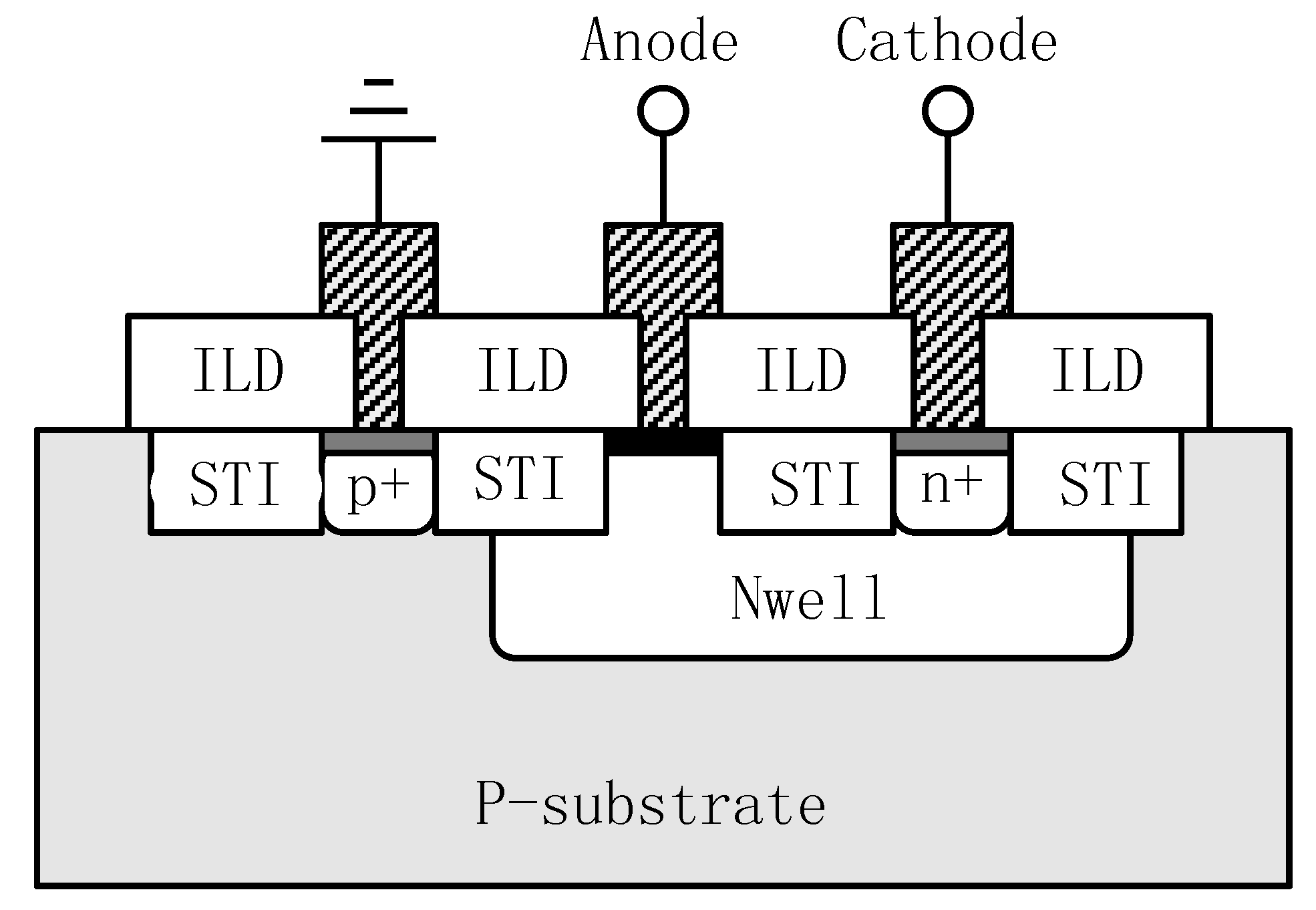
Figure 1 shows the cross section of the Schottky barrier diode without any process modifications in 0.13 μm SiGe BiCMOS. The diode is fabricated in an
n-well as the figure shows. The Schottky contact is formed on the diffusion region where there are no implants. The ohmic contacts are formed on
n implanted parts of an
n-well. The anode and cathode are also shown with metal connections. The static current
IA of the diode is expressed as Equation (1) shows:
where
IS is the reverse saturated current,
n is the ideality factor,
VAC is the voltage applied on the diode,
RS is the parasitic series resistance, K is the Boltzmann constant,
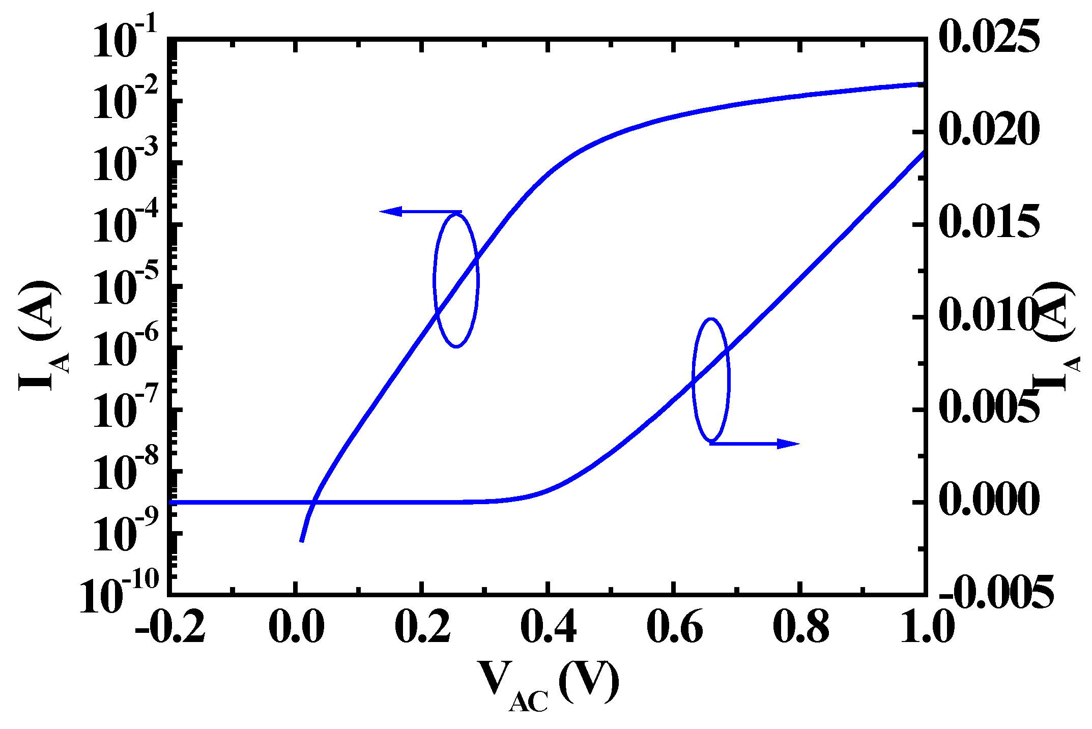
T is the temperature in Kelvin. The simulated DC sweep of the SBD with dimension of 1 μm × 0.3 μm is depicted in
Figure 2, from which a reverse saturated current of 2.06 nA and an ideality factor of 4.135 are calculated. Also, a series resistance of 26.3 Ohm, and zero bias junction capacitance of 20 fF are calculated from simulation which implies a cut-off frequency of 302 GHz.
Figure 1.
Cross section of the Schottky barrier diode.
Figure 1.
Cross section of the Schottky barrier diode.
Figure 2.
Simulated DC response of the Schottky barrier diode (SBD) with dimension of 1 μm × 0.3 μm.
Figure 2.
Simulated DC response of the Schottky barrier diode (SBD) with dimension of 1 μm × 0.3 μm.
3. Circuit Design
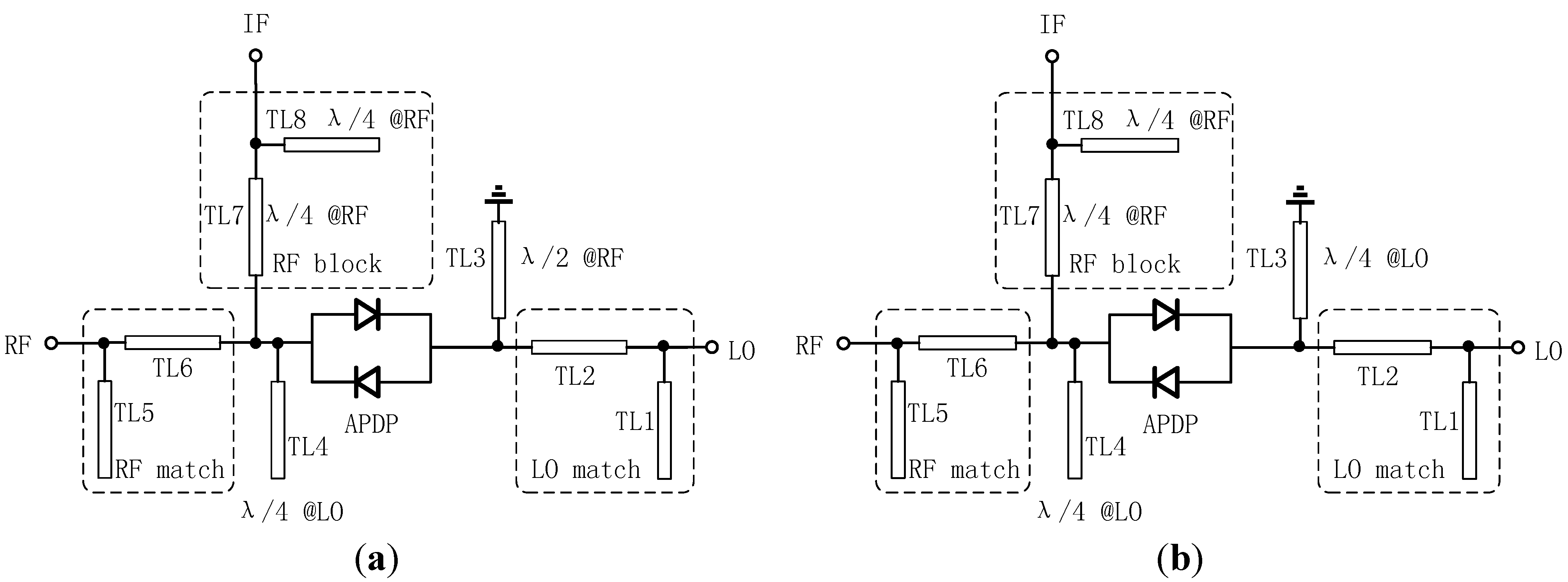
The topologies of the designed SHMs are shown in
Figure 3. APDP is used as the mixing core and micro-strip transmission lines (TLs) are deployed for impedance matching. The IF frequency (
fIF) of the SHM can be expressed as follows [
4]:
In our proposed design, the 2nd and the 4th harmonics of the LO signal are used for mixing so that the radio frequency (RF) frequency is about 2 and 4 times of the LO frequency. At the LO port in
Figure 3a, TL3, the half wave length shorted stub at RF frequency acts as both a shorted circuit for RF frequency and an opened circuit for LO frequency, so that RF signals are shorted but LO signals are not affected. At LO port in
Figure 3b, TL3, the quarter wave length shorted stub at LO frequency acts as both a shorted circuit for RF frequency and an opened circuit for LO frequency.
Figure 3.
Topology of the 340 GHz sub-harmonic down-mixers: (a) 2× sub-harmonic mixer (SHM) and (b) 4× SHM.
Figure 3.
Topology of the 340 GHz sub-harmonic down-mixers: (a) 2× sub-harmonic mixer (SHM) and (b) 4× SHM.
Similarly, at RF port, TL4, an open quarter wave length shunt stub at LO frequency, forms the grounding path for LO signals and open for RF signals. Transmission lines, TL1 and TL2, are the LO match network; transmission lines TL5 and TL6, are the RF match network. At IF port, TL8, an open quarter wave length transmission line at RF frequency and TL7, a series quarter wave length transmission line at RF frequency serve as the RF choke.
Concern that the 4× SHM is to use the 4th harmonic of the LO signal to pump the APDP; the LO-RF isolation is inherently larger than its 2nd harmonic counterparts due to the huge difference between the RF and LO frequencies.
The TLs used are fabricated by the top metal layer with the thickness of 3 μm and the ground metal with the thickness of 0.4 μm; the space between the two is 9.83 μm. All the transmission lines in this design have the characteristic impedance of 50 Ohm, with the strip width of 16 μm. The simulation is done with extensive EM simulations by High Frequency Structure Simulator (HFSS) along with the SBD model in Advanced Design Systems (ADS) provided by the Process Design Kit (PDK).
4. Measurement and Discussion
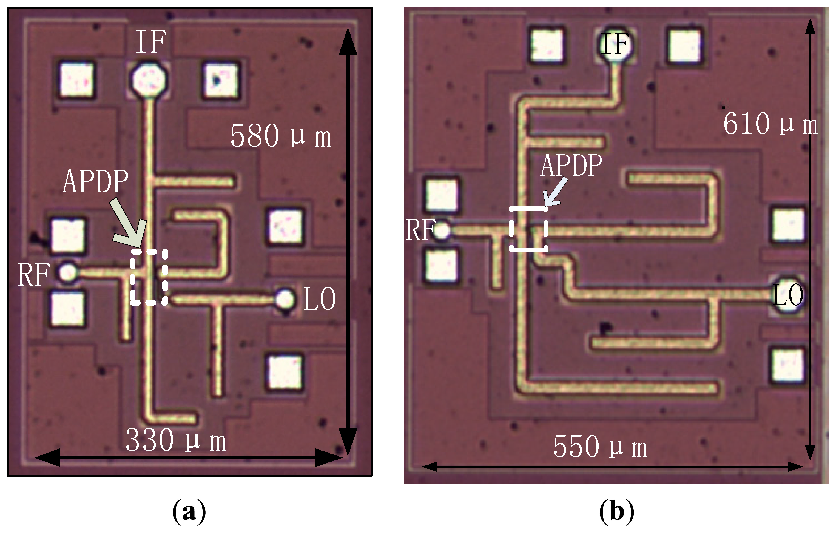
Figure 4 shows the die photographs of the two fabricated 340 GHz SHMs, with the dimensions of 330 μm × 580 μm and 550 μm × 610 μm including the testing pads. The SHMs are measured on wafer with ground-signal-ground (GSG) probes.
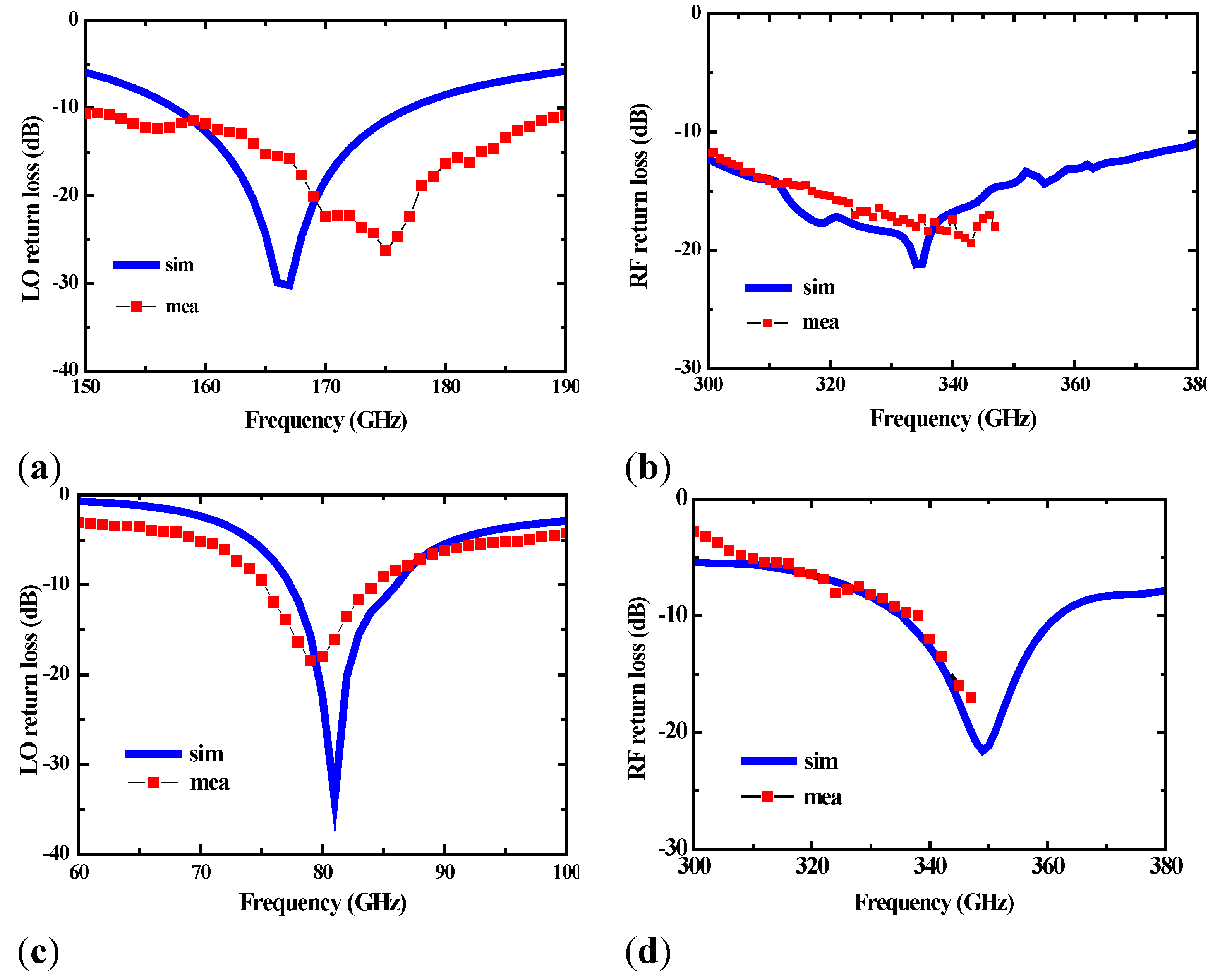
The S-parameters are measured with an Agilent vector network analyzer (VNA) and a VDI extender up to 347 GHz. The measured and simulated LO and RF return losses are depicted in
Figure 5. The LO return losses of the 2× SHM show slight frequency drift towards higher frequencies whereas the LO return losses of the 4× SHM show frequency drift towards lower frequencies, as shown in
Figure 5a,c, respectively. However, the impedance matching for the LO signals are good enough at the central frequencies of 170 GHz and 85 GHz for the two mixers. The measured RF return losses are limited to 347 GHz. However, it can be seen that the measured and simulated results are in good agreement throughout the measured frequency range.
Figure 4.
Die photographs of the 340 GHz SHMs: (a) 2× SHM and (b) 4× SHM.
Figure 4.
Die photographs of the 340 GHz SHMs: (a) 2× SHM and (b) 4× SHM.
Figure 5.
Measured and simulated S parameters of the 2× and 4× SHMs: (a) Return losses at LO port of the 2× SHM; (b) return losses at RF port of the 2× SHM; (c) return losses at LO port of the 4× SHM; and (d) return losses at RF port of the 2× SHM.
Figure 5.
Measured and simulated S parameters of the 2× and 4× SHMs: (a) Return losses at LO port of the 2× SHM; (b) return losses at RF port of the 2× SHM; (c) return losses at LO port of the 4× SHM; and (d) return losses at RF port of the 2× SHM.
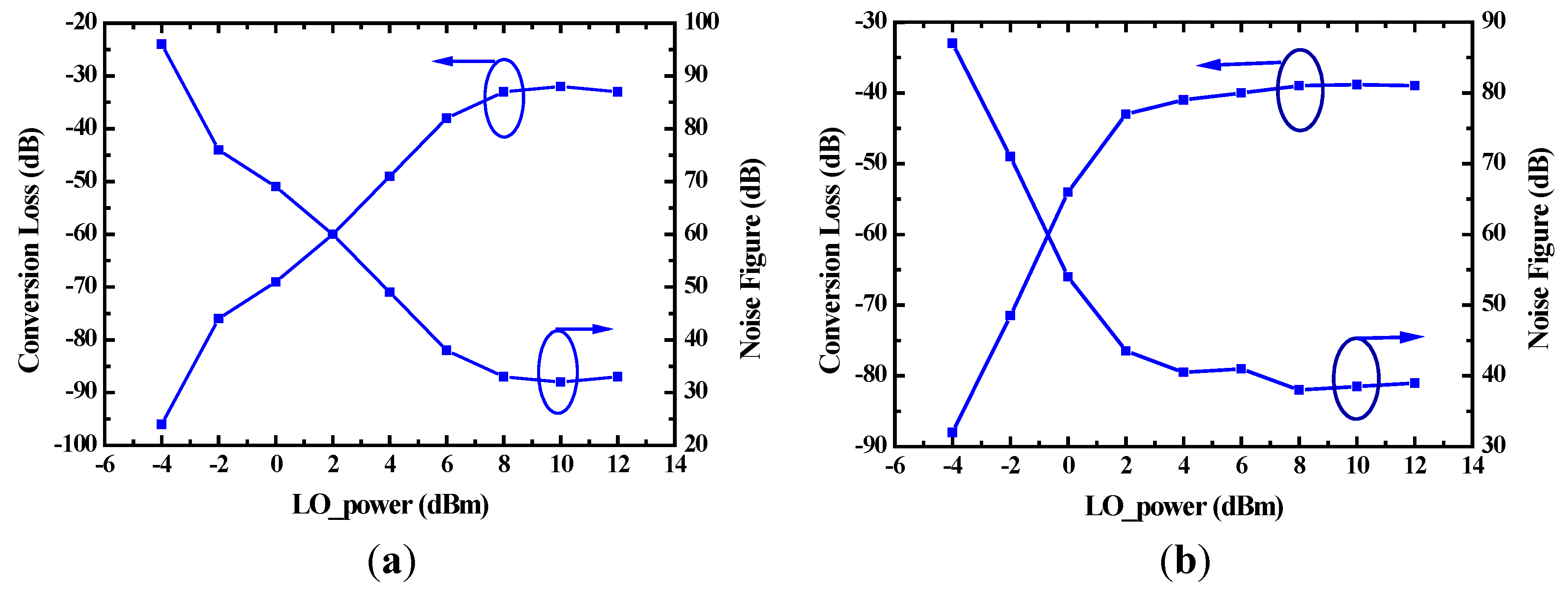
For achieving better down-mixing performance, a proper LO power is needed to pump the SHM to result in less conversion loss and lower noise figure (NF). At the RF frequency of 335 GHz and LO frequencies of 170 GHz or 85 GHz, the simulated conversion loss and NF
versus LO power for both of the mixers are depicted in
Figure 6. For the 2× SHM, the optimal LO power is about 10 dBm from simulation. However, 7 dBm is used during measurement due to the limitation of the 170 GHz signal source. And for the 4× SHM, the simulated optimal LO power is 8 dBm; and the measured optimal LO power is 9 dBm.
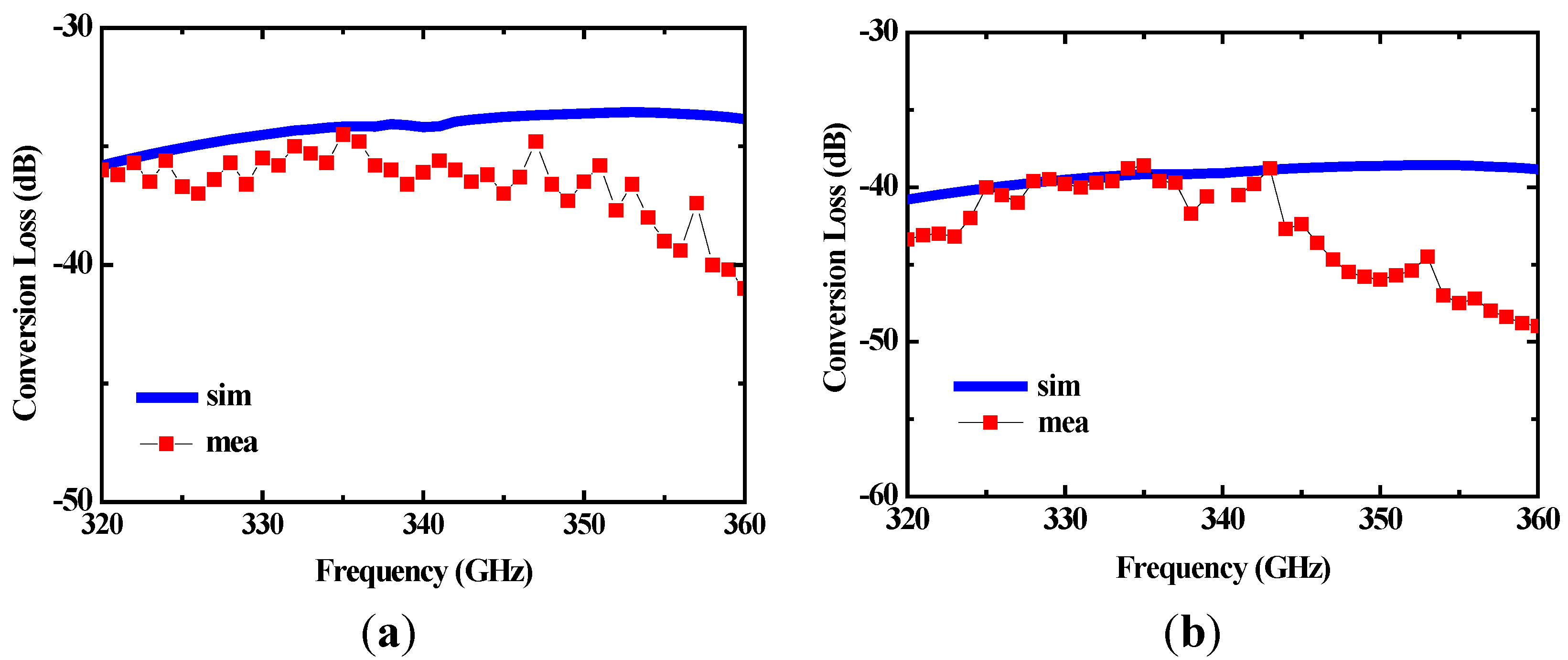
Figure 7 depicts the measured and simulated conversion losses of the two SHMs when the LO frequency is fixed at 170 GHz with 7 dBm power or at 85 GHz with 9 dBm power. For the 2× SHM, the measured lower band (320–340 GHz) conversion loss is 34.5–37 dB, which is about 2-dB larger than the simulation results on average. For the 4× SHM, the measured lower band (320–340 GHz) conversion loss is 39–43 dB, which is in good agreement with the simulated result; but the measured conversion loss for the upper band (340–360 GHz) is 40–48 dB, which is much larger than the simulated results. This may be due to the model inaccuracies of the Schottky barrier diode.
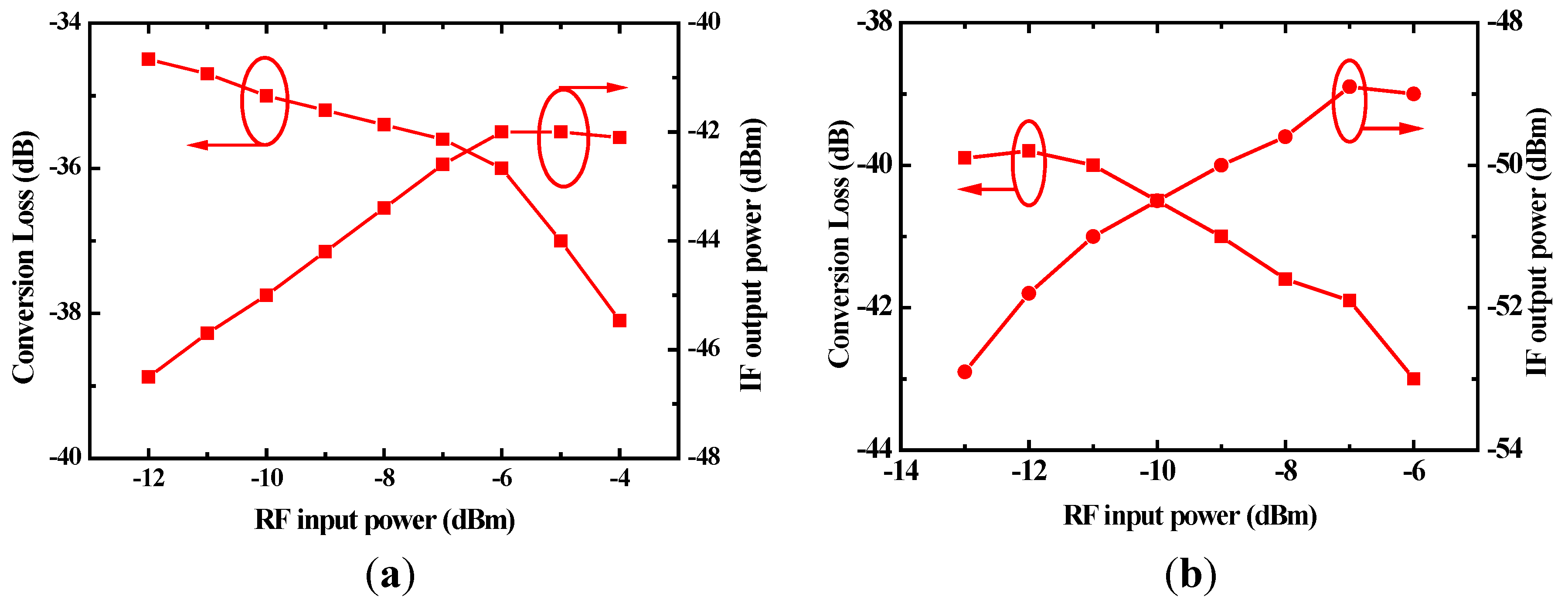
The conversion losses and IF output power
versus the RF input power measured at 325 GHz for the two mixers are illustrated in
Figure 8, which shows that the measured input 1-dB compression point is −8 dBm and −10 dBm for the 2× SHM and 4× SHM, respectively.
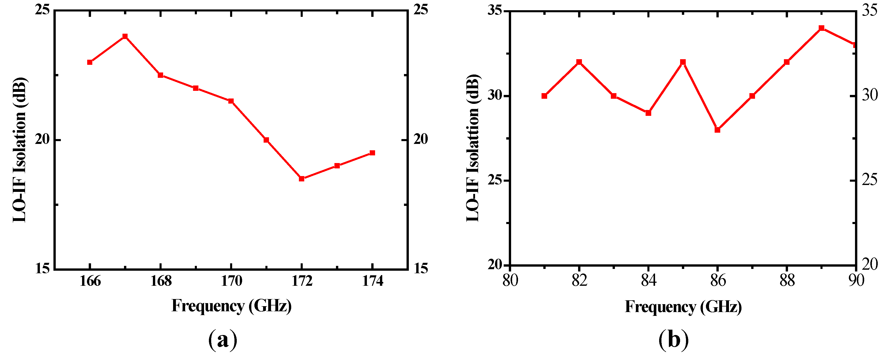
At the LO frequency of 80–90 GHz, the measured LO-IF isolation of the 4× SHM is depicted in
Figure 9b. More than 28-dB isolation is achieved in the corresponding frequency range. In our measurement setup, coaxial cables are used to connect the probes lower than 110 GHz, while waveguides are used to connect the probes higher than 110 GHz. As a result, the measurement of the 2× SHM LO-IF isolation is not applicable, since the 170 GHz LO signal is heavily suppressed at the IF port due to the low pass feature of the coaxial cable. The simulated LO-IF isolation for the 2× SHM is presented in
Figure 9a instead.
Figure 6.
Simulated conversion loss and noise figure (NF) versus LO power: (a) 2× SHM and (b) 4× SHM.
Figure 6.
Simulated conversion loss and noise figure (NF) versus LO power: (a) 2× SHM and (b) 4× SHM.
Figure 7.
Measured and simulated conversion loss of the SHM: (a) 2× SHM and (b) 4× SHM.
Figure 7.
Measured and simulated conversion loss of the SHM: (a) 2× SHM and (b) 4× SHM.
Figure 8.
Measured conversion loss and IF output power versus RF power: (a) 2× SHM and (b) 4× SHM.
Figure 8.
Measured conversion loss and IF output power versus RF power: (a) 2× SHM and (b) 4× SHM.
Figure 9.
LO-IF port isolation: (a) simulated isolation of 2× SHM and (b) measured isolation of 4× SHM.
Figure 9.
LO-IF port isolation: (a) simulated isolation of 2× SHM and (b) measured isolation of 4× SHM.
The simulated SSB NF of the two mixers are 34–36 dB and 39–41 dB within 320–360 GHz. The actual NF is estimated to be about the same value of measured conversion loss due to the passive topology of SHMs.
Performance comparison between some reported APDP-based SHMs and this work is shown in
Table 1. Comparing with the 94 GHz 4× SHM [
4] and 122 GHz 2× SHM [
5], our proposed SHMs work at much higher RF frequency. Comparing with the 245 GHz 2× SHM, our proposed 4× SHM requires a LO at lower frequency. The drawback of the proposed 2× SHM and 4× SHM is their high conversion loss due to the SBD’s low cut-off frequency provided by the foundry. Furture work shall be done to modify the SBD layout to increase the cut-off frequency, which will result in lower conversion loss of the sub-harmonic mixer.
Table 1.
Performance comparison of anti-parallel-diode-pair (APDP)-based SHMs.
Table 1.
Performance comparison of anti-parallel-diode-pair (APDP)-based SHMs.
| Reference | [4] | [5] | [6] | This work |
|---|
| Technology | GaAs | SiGe | SiGe | SiGe | SiGe |
| RF Frequency (GHz) | 94 | 122 | 245 | 340 | 340 |
| Die Size (mm2) | 1.3 | 0.6 | 0.56 | 0.19 | 0.34 |
| LO Power (dBm) | 10@RF/4 | 5@RF/2 | 6.5@RF/2 | 7@RF/2 | 9@RF/4 |
| Input P1dB (dBm) | −6 | −5 | Not Available | −8 | −10 |
| Conversion Loss (dB) | 11.4 | 8 | 17 | 34.5–37 * | 39–43 * |


