1. Introduction
Gallium and its compounds can find many applications in microelectronics [
1], solar cells [
2,
3], solar water splitting [
4,
5], microwave circuitry [
6], optoelectronics [
7], flexible neuroprobes [
8], self-repairing electrodes [
9], and micro switches [
10]. Considerable efforts have already been made to deposit gallium thin films, which typically involve electroplating with highly toxic gallium salts. For example, as a critical precursor layer of CuIn
xGa
(1−x)Se
2 (CIGS) solar cells, Ga–Cu alloy was co-electroplated by employing a solution of GaCl
3 and CuCl
2 in an ionic liquid electrolyte. The rate of Ga electroplating is typically slow, e.g., approximately 2 μm/30 min or 0.067 μm/min on molybdenum substrate [
11]. The composition control can also be challenging since the deposition rate of different species are mainly controlled by their respective electrochemical potentials. High-quality Ga thin film can also be obtained by physical vapor deposition (PVD), while some Ga compounds thin films, such as gallium arsenide (GaAs) and gallium nitride (GaN), can be obtained by chemical vapor deposition (CVD) [
12] and pulsed laser deposition [
13]. However, the high cost, low deposition rate and poor scalability have limited the employment of those aforementioned methods in applications, such as solar cells.
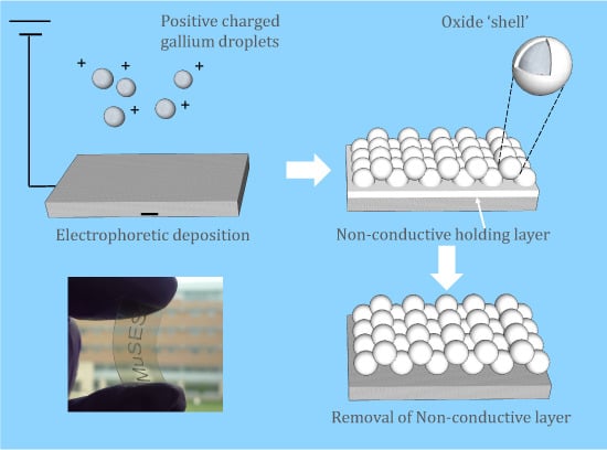
Electrophoretic deposition (EPD) is known for its low cost, versatility and excellent scalability [
14]. The deposition relies on the net charges, as part of the electric double layers (EDLs), on the surface of particles that are dispersed in a liquid medium. When subjected to an electric field, the charged particles can be moved to the oppositely-charged electrode and get deposited. The deposition rate is thus independent of the reduction potential of the species being deposited. As compared with electroplating, whose deposition rate strongly depends on the reduction potential of the species being deposited, the deposition rate control of EPD is more straightforward, which makes it more suitable for co-deposition [
15]. EPD can also be performed to deposit gallium on various substrates as precursors to obtain the aforementioned functional materials. Recently, successful electrophoretic deposition of rare earth doped GaN thin film was reported to have enhanced infrared photoluminescence intensity [
16]. In this work, we communicate successful EPD of Ga thin film with a high deposition rate of ~0.6 μm/min (~9 times of the typical value reported for electroplating [
11]). The critical deposition parameters and process compatibility to micro patterning are also investigated.
2. Experimental Section
Gallium (Alfa Aesar, 99.9% purity, Ward Hill, MA, USA) with a melting point of ~29.9 °C, can be either liquid or solid depends on the ambient temperature. If it is in solid phase, gallium was first melted by heating and then dispersed in isopropyl alcohol (IPA) (Pharmco-AAPER, 99% purity, Brookfield, CT, USA) at a concentration of 0.5 mg/mL by sonication at a power of 130 W for 25 min with an ultrasonic processor (Sonics and Materials Inc., VCX130, Newtown, CT, USA). In order to keep the dispersion stable and facilitate EPD, magnesium nitrate hexahydrate (Fisher Scientific, 99% purity, Hampton, NH, USA) was also added to charge the gallium droplets. The stability of the dispersion was improved by quenching the dispersion to a lower temperature so that the gallium can be solidified while the viscosity of IPA was increased [
17]. The quenching was achieved by directly adding dry ice into the dispersion right after sonication. By doing this, the temperature of the dispersion was brought down to −30 °C within 1 min. The dispersion was sonicated again by an ultrasonic cleaner (Branson Ultrasonics Corporation, Bransonic 1510, Danbury, CT, USA) at a lower power of 70 W for a few minutes in order to further stabilize it. Compare to the sonication of the dispersion without quenching, significant bubble generation in quenched dispersion was observed during sonication. The hypothesis is that those bubbles were generated by ultrasonic degassing of carbon dioxide from the mixture during quenching process. After sonication, dispersion was stored at −15 °C for stability characterization.
With a stable dispersion, EPD was performed at −15 °C in a salt ice bath [
18] (17 wt % CaCl
2 aqueous solution) with two stainless steel plates (25 mm × 19 mm × 2 mm) as the electrodes. An electric field of 600 V/cm was supplied by a high voltage power source (Stanford Research System Inc., Model PS 325/2500 V-25 W, Sunnyvale, CA, USA). The charging salt, Mg(NO
3)
2, dissolved in IPA, was also co-deposited as magnesium compounds (see next section for details), which can be removed by weak acetic acid after EPD. The deposited samples were observed under a field emission scanning electron microscope (FESEM) with energy dispersed spectroscopy (EDS) capability (Hitachi, Hitachi S-4700, Tokyo, Japan). The particle size was analyzed by software ImageJ 1.48 (National Institute of Health, Bethesda, MD, USA) from the FESEM image. The weight of the deposit was measured by a high-precision (0.1 mg resolution) analytical balance (Adam Equipment Inc., PW124, Danbury, CT, USA) and the thickness of the deposit was measured by a laser profile scanner (Optical Gaging Products, Cobra, Rochester, NY, USA). A cutter (Silhouette American Inc., Silhouette CAMEO, Orem, UT, USA) was used to pattern adhesive-loaded vinyl tapes (Silhouette American Inc.) as the masks for Ga micro patterning.
3. Results and Discussion
A stable dispersion is normally required for a uniform deposition, as EPD of an unstable dispersion may lead to coagulation of particles [
19]. Gallium, as a metal with a relatively low melting point of 29.9 °C, forms liquid droplets in the dispersion after sonication as a result of ultrasonic heating. A similar process to prepare gallium colloid by ultrasound has been demonstrated lately [
20]. It has been observed that the dispersion normally reached a temperature of ~50 °C after 1 min of the aforementioned sonication process. Unfortunately, different from solid particles, the liquid gallium droplets can easily coagulate with each other shortly after the sonication. Such a colloid of gallium at room temperature completely collapses within a few hours, as evidenced by the precipitate observed on the bottom of the testing tube (
Figure 1a) and the clear liquid seen at the side (
Figure 1c) after 2 h. With quenching of the dispersion and storage at −15 °C, no significant precipitate has been observed on the bottom of the testing tube after two hours (
Figure 1b) while the side view still remain cloudy (
Figure 1d). The observation indicates improved stability of at least 2 h at −15 °C, which is later proved to be sufficient for successful EPD. The dispersion has also been stored in a freezer (Kendro Laboratory Products, Isotemp Basic, Hanau, Germany) at about −75 °C, where it can remain stable for three days. Our observation on improved dispersion stability at low temperature agrees with previous reports on obtaining gallium-organic solvent dispersions by co-condensation at low temperature (
i.e., 77 K), where IPA has been identified as the preferable solvent for high stability [
21].
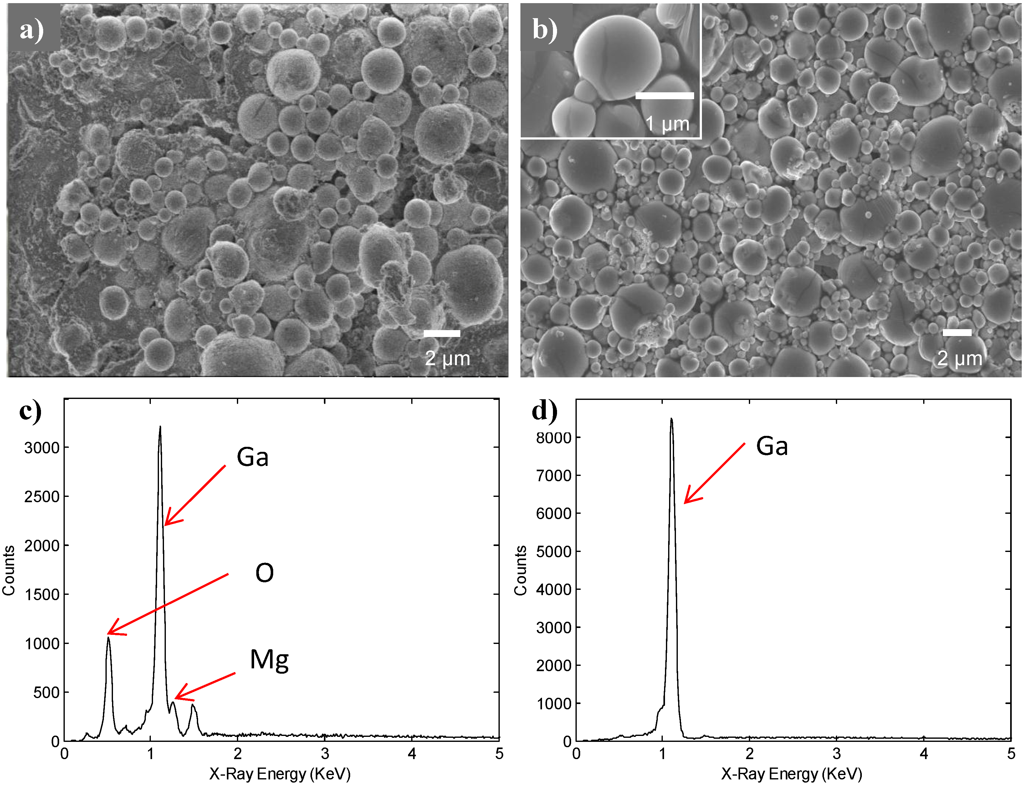
After EPD, deposition was found on the negative electrode, which indicates that gallium particles were positively charged by Mg
2+ ions. The deposited film was translucent with rainbow-colored reflection and near-spherical gallium particles can be observed under FESEM, as
Figure 2a,b shows. During EPD, the charging salt Mg(NO
3)
2 also forms Mg(OH)
2 and Mg(C
3H
7O)
2 near the electrode, which can serve as a co-deposited holding layer [
22,
23]. Both of the two compounds are non-conductive, rendering their whitish color under FESEM. To improve conductivity and remove impurities, the samples were carefully rinsed by weak acetic acid. It is noticed that the film had a whitish color in air, which can be attributed to the surface oxidation of gallium [
24,
25]. During FESEM imaging, when an electron beam with a strong enough accelerating voltage was focused on a particular particle, melting and crack formation (the insert of
Figure 2b) was observed on the thin oxidation 'shell' of the gallium particles.
Figure 2c shows the EDS data with a major peak of gallium and smaller peaks of magnesium and oxygen from the co-deposited compounds, while the EDS data of the sample after washing with acetic acid (
Figure 2d) only shows the Ga peak. It should be noticed that the EDS result only confirms the removal of the exposed Mg-based holding layer. Further analysis like inductively coupled plasma mass spectrometry (ICP-MS) should reveal if there is still Mg-based compound left between the particles. More vigorous washing procedure should be developed if any application is sensitive to Mg impurity. By analyzing FESEM images with ImageJ, the average particle size was determined to be 727 nm. The size distribution was observed to be broad, with a high standard deviation of 408 nm, which can be partly attributed to the uneven power distribution of sonication and coagulation of gallium nano-droplets during handling.
Native gallium droplets dispersed in IPA solution carry weak negative charges, which are not sufficient to keep the dispersion stable for reliable EPD process. Therefore, Mg(NO
3)
2 is added to the dispersion as the charging salt. The concentration of Mg(NO
3)
2 plays a critical role on the dispersion stability and the deposition rate. To get reliable, high-quality depositions, the Mg
2+ ions should be enough to charge the gallium particles yet not too high. Otherwise, the excessive ionic strength could thin the electric double layer and tend to destabilize dispersion [
14,
26]. Meanwhile, high concentration of Mg
2+ may result in the quick formation of the non-conductive layer, leading to a lower deposition rate.
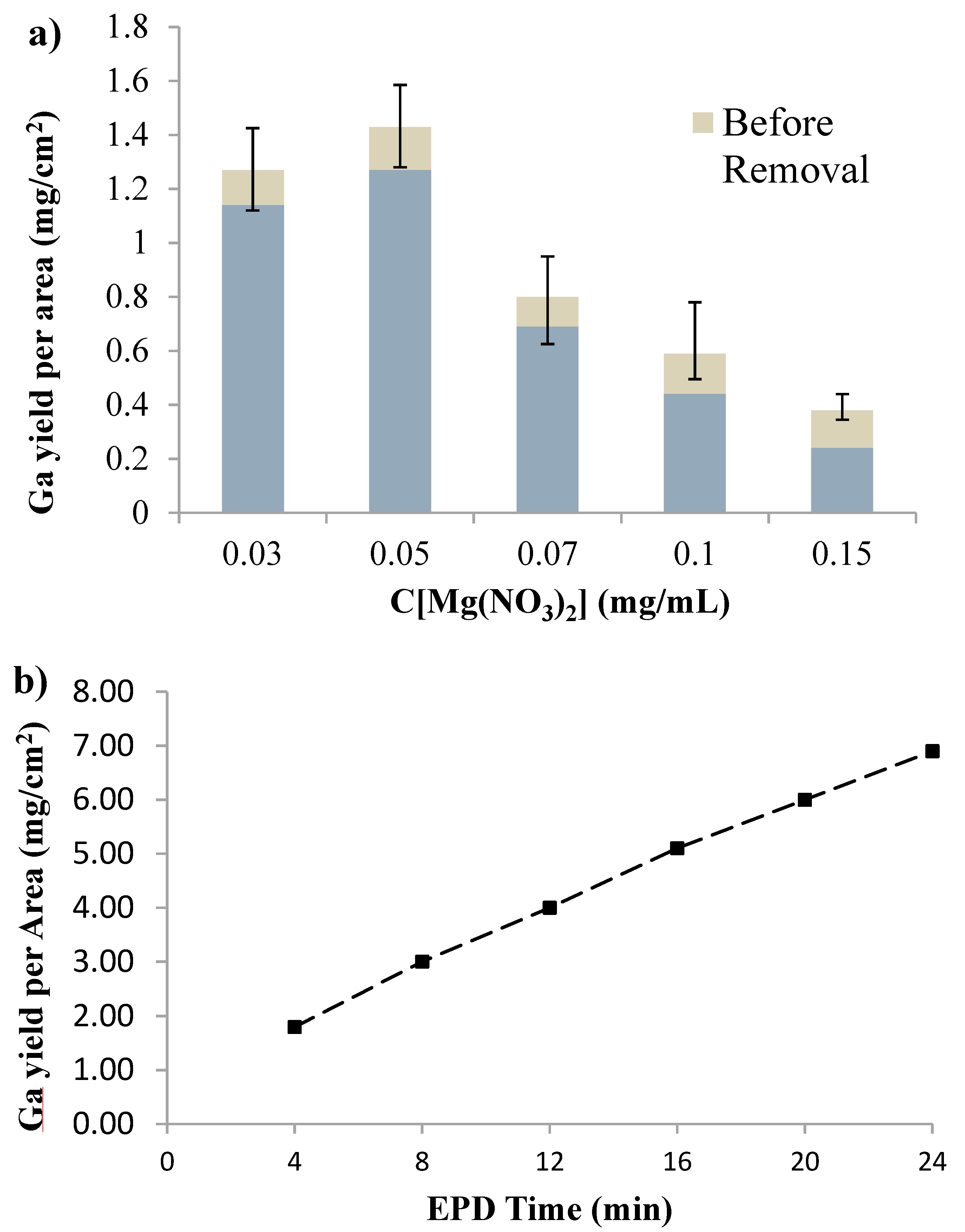
It is thus hypothesized that the concentration of magnesium nitrate, C[Mg(NO
3)
2], has significant impact on the deposition rate. To test such hypothesis, EPD was performed with different C[Mg(NO
3)
2] values while other key parameters were kept constant. The results are shown in
Figure 3. The average areal yield reached a peak of m/A = 1.43 mg/cm
2 at C[Mg(NO
3)
2] = 0.05 mg/mL, which supported the hypothesis and provided a set of appropriate deposition parameters. Similar pattern of maximum yield at an optimal concentration of charging agent was observed for EPD of phosphor by Shane
et al. [
27]. A typical weight reduction of ~0.14 mg/cm
2 (~10%) was also noticed after rinsing with the weak acid. The weight reduction can be attributed to the loss of non-conductive Mg compounds holding layer and small amount of gallium lost during the rinsing process.
In order to compare to the reported deposition rate of gallium electroplating (~0.067 μm/min), the thickness of the electrophoretic deposited film was both indirectly calculated and experimentally measured. The thickness of the film (
L) was first estimated by:
where
m is the mass of the film;
A is the area of the film (
m/
A = 1.27 mg/cm
2) and ρ is the density of gallium (5.91 g/cm
3), resulting in a value of
Lmin = 0.215 × 10
−3 cm = 2.15 μm. However, since the Ga film is not a perfectly dense film, the actual thickness may be up to
Lmax =
Lmin/(4/3·π·0.5
3) = 4.11 μm (assuming all deposited gallium are spherical particles with exactly same diameters). Since the deposition was four minutes, the deposition rate was thus estimated to be 0.5–1.0 μm/min. The thickness of this film was also directly measured as 2.4 μm by a laser profile scanner, resulting in a deposition rate of ~0.6 μm/min which falls into the range of rate estimated from the mass. The deposition rate is almost one order of magnitude higher than the previously-reported deposition rate of electroplating (~ 0.067 μm/min) [
11].
Figure 1.
Stability of gallium-IPA dispersion before ((a) and (c), labeled as RT for room temperature) and after (b) and (d) being quenched by dry ice. The status of samples at 0, 1 and 2 h after sonication is shown. The stability can be judged by whether precipitate is formed on the bottom (a) and (b) and whether the side view turns clear (c) and (d).
Figure 2.
Field emission scanning electron microscope (FESEM) images and energy dispersed spectroscopy (EDS) analysis of the deposition: (a) gallium particles with magnesium compounds holding layer; (b) gallium particles after the removal of magnesium compounds and a magnified view of a few particles showing cracks on the oxide “shell” as inset; (c) EDS of the film before removal of magnesium compounds; and (d) EDS of the film after removal of magnesium compounds.
Figure 3.
(a) The deposition yield as related to different concentration of Mg(NO3)2. Deposition time: 4 min; (b) Sequential deposition to increase film thickness. Electric field strength: 600 V/cm; concentration of Mg(NO3)2: 0.05 mg/mL; Concentration of gallium: 0.5 mg/mL; Temperature: −15 °C.
Figure 3.
(a) The deposition yield as related to different concentration of Mg(NO3)2. Deposition time: 4 min; (b) Sequential deposition to increase film thickness. Electric field strength: 600 V/cm; concentration of Mg(NO3)2: 0.05 mg/mL; Concentration of gallium: 0.5 mg/mL; Temperature: −15 °C.
Relatively thick (e.g., tens of μm) Ga films can be desirable in many applications, including liquid metal electrodes [
8,
9] and micro switches [
10]. Sequential deposition was performed to verify such capability of the reported method and address the concern of self-limited deposition caused by the non-conductive holding layer, which is intentionally kept without being rinsed in this case. The deposition was divided into multiple steps, while each step was kept at four minutes to avoid destabilization of the dispersion under extensive EPD. The dispersion was also sonicated for five minutes between each step to maintain its stability. The stainless steel plate substrate with the deposited film was dried and weighted after each deposition. The differences between each measurement were taken to determine the total yield, which includes the weight of both gallium and Mg compounds in the thin film. The concentration of the magnesium nitrate in the dispersion was 0.05 mg/mL, which has been verified previously as the optimal EPD parameters in this particular experiment. The electrical field strength and temperature were kept as 600 V/cm and −15 °C respectively. As shown in
Figure 3b, the deposition rate was not significantly reduced after 24 min of total deposition time (six steps), when the total yield reached 6.9 mg/cm
2 (12.6 μm). To eliminate the impact caused by decrease of gallium concentration in this experiment, after the third step, the dispersion was replaced by a fresh one which was identical with the dispersion at the beginning of the experiment. It should be noticed that deposition was carried out without removing the non-conductive holding layer between the deposition steps. The yield reported in
Figure 3b, thus, includes Mg compounds, which can be removed later by acid washing. It was also noticed that removal of the non-conductive holding layer by weak acid between each two deposition steps could eventually lead to a slightly higher gallium yield in this experiment. However, multiple rinsing steps led to severe roughening of the deposit and loss of Ga, which is not desirable. Therefore, it is demonstrated that the reported technique can be used to obtain thick film without significantly reduced deposition rate.
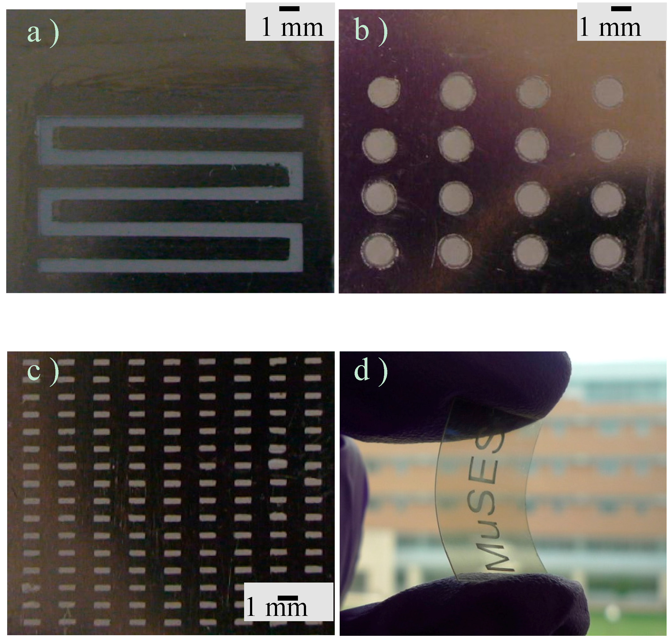
As previously mentioned, gallium and its compounds can find many applications in electronic devices and flexible electrodes. The EPD method reported herein can potentially offer a low-cost, less complex and scalable alternative to conventional vapor deposition processes and recently reported injecting and printing processes of delicate gallium patterning [
28,
29]. In order to verify its compatibility with micropatterning technology for such applications, several gallium micro patterns were obtained by masking the substrate during EPD. In particular, gallium micropatterns with feature size ranging from 300 μm (
Figure 4c) to 2 mm (
Figure 4b) were formed on the stainless steel and flexible ITO (Indium tin oxide) coated film (MTI Corporation, Richmond, CA, USA) substrates. In this case, the vinyl tape mask was used and promptly removed after deposition, followed by carefully rinsing the samples with acetone to remove the residue of adhesive. Finally, if needed, the holding layer (Mg compounds) can also be removed by diluted acetic acid.
Figure 4.
Various patterns of gallium on stainless steel substrates: (a) 1 mm-wide serpentine lines; (b) circles of 2 mm in diameter; (c) an array of 1 mm × 300 μm rectangular bars. (d) Letters on flexible substrate.
Figure 4.
Various patterns of gallium on stainless steel substrates: (a) 1 mm-wide serpentine lines; (b) circles of 2 mm in diameter; (c) an array of 1 mm × 300 μm rectangular bars. (d) Letters on flexible substrate.

