A CMOS Time-Resolved Fluorescence Lifetime Analysis Micro-System


Abstract
:
1. Introduction
2. Background
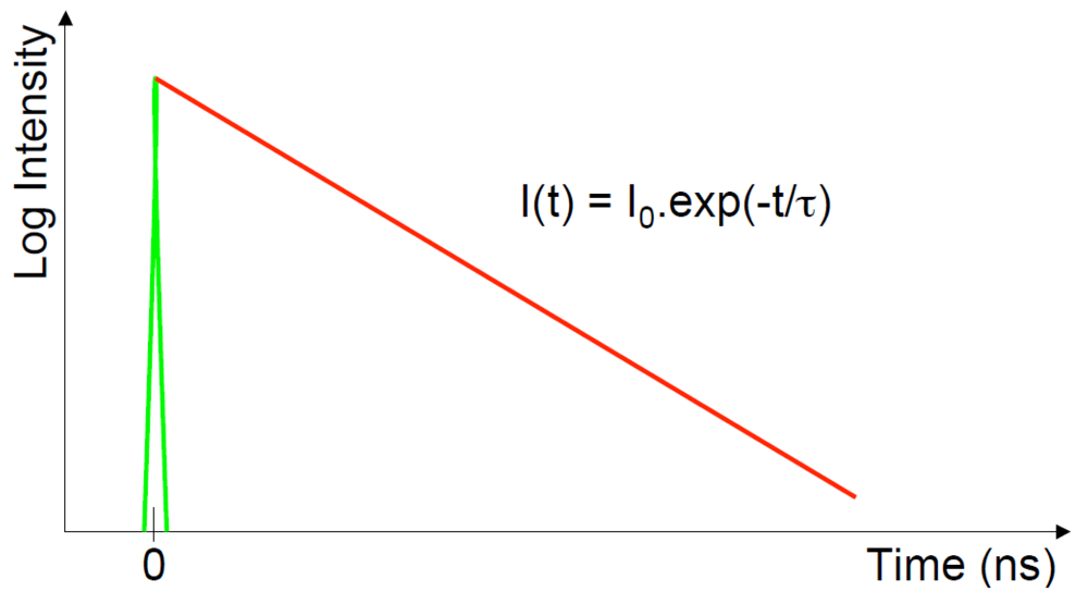
2.1. Fluroescence Lifetime
- Inter-system crossing
- Collisional or static quenching
- Solvent effects
- Resonance energy transfer.
2.2. Excitation Sources
2.3. Detectors
2.4. Miniaturisation
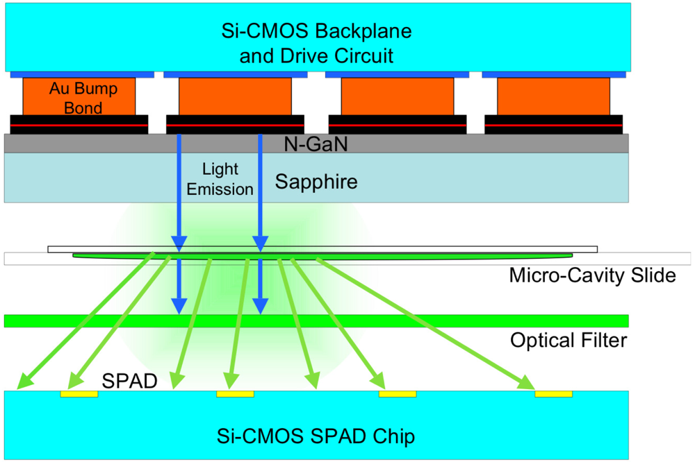
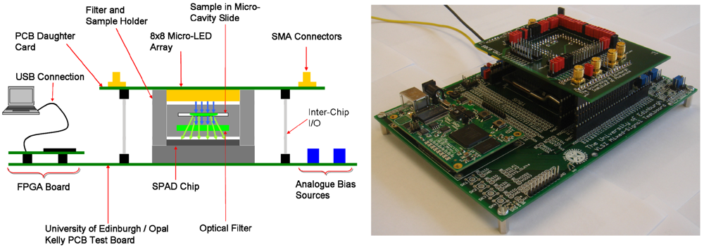
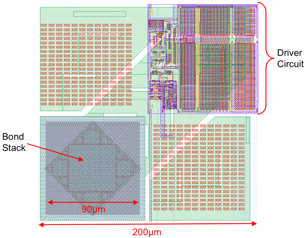
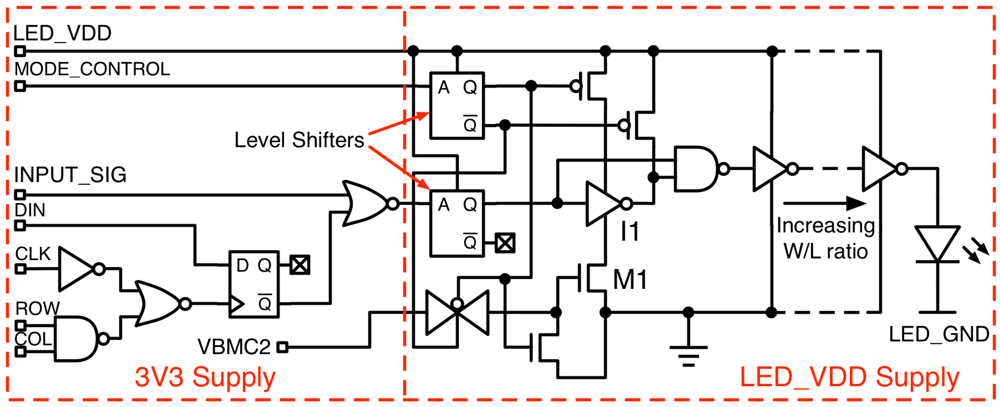
3. Device Implementation
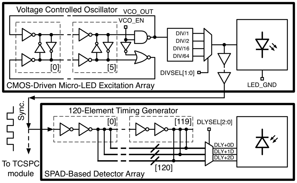
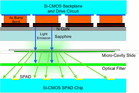
3.1. Excitation Array
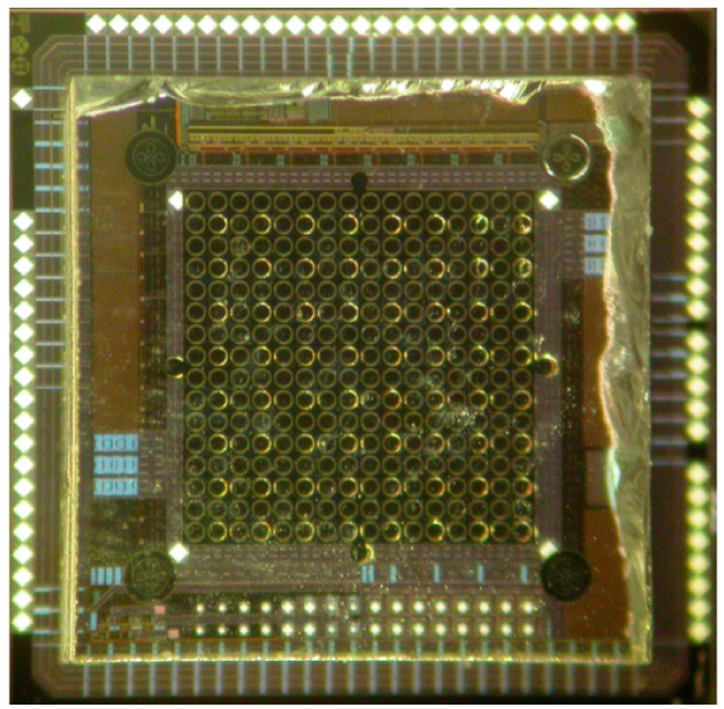
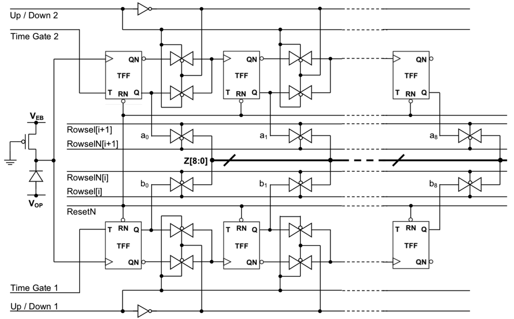
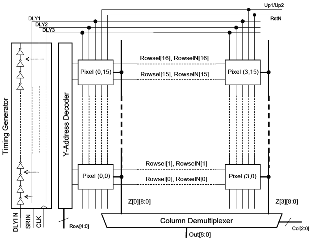
2.2. Detection Array
4. System Configuration
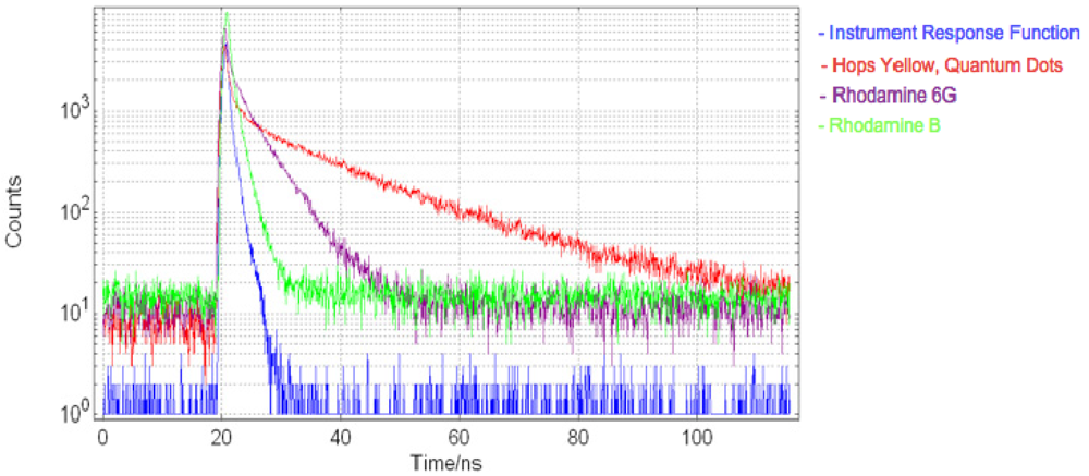
4. Results
5. Conclusions
Acknowledgments
References and Notes
- Rochas, A.; Gani, M.; Furrer, B.; Besse, P.-A.; Popovic, R. Single photon detector fabricated in a complementary metal-oxide-semiconductor high-voltage technology. Rev. Sci. Instrum. 2003, 74, 3263. [Google Scholar]
- Choi, H.W.; Jeon, C.W.; Dawson, M.D.; Edwards, P.R.; Martin, R.W. Fabrication and performance of parallel-addressed InGaN micro-LED arrays. IEEE Photonics Technol. Lett. 2003, 15, 510–512. [Google Scholar]
- Li, D.-U.; Bonnist, E.; Renshaw, D.; Henderson, R. On-chip, time-correlated, fluorescence lifetime extraction algorithms and error analysis. J. Opt. Soc. Am. A 2008, 25, 1190–1198. [Google Scholar]
- Li, D.-U.; Walker, R.; Richardson, J.; Rae, B.; Buts, A.; Renshaw, D.; Henderson, R. Hardware implementation and calibration of background noise for an integration-based fluorescence lifetime sensing algorithm. J. Opt. Soc. Am. A 2009, 26, 804–814. [Google Scholar]
- Patounakis, G.; Shepard, K.; Levicky, R. Active CMOS biochip for time-resolved fluorescence detection. Symp. VLSI Circuits Digest of Technical Papers. 2005, 68–71. [Google Scholar]
- Turconi, S.; Bingham, R.P.; Haupts, U.; Pope, A.J. Developments in fluorescence lifetime based analysis for ultra-HTS. Drug Discov. Today 2001, 6, 27–39. [Google Scholar]
- Lakowicz, J. Principles of Fluorescence Spectroscopy, 3rd ed.; Springer: New York, NY, USA, 2006. [Google Scholar]
- Christenson, M.; Sternberg, S. Fluorescence lifetime imaging microscopy (flim) lets biologists study cellular processes. SPIE's oemagazine 2004. [Google Scholar] [CrossRef]
- Pepperkok, R.; Squire, A.; Geley, S.; Bastiaens, P. I. H. Simultaneous detection of multiple green fluorescent proteins in live cells by fluorescence lifetime imaging microscopy. Curr. Biol. 1999, 9, 269–274. [Google Scholar]
- Prasad, P.N. Introduction to Biophotonics, 1st ed.; Wiley-Interscience: New York, NY, USA, 2003. [Google Scholar]
- Chodavarapu, V.; Khanol, S.; Tehan, E.; Titus, A.; Cartwright, A.; Bright, F. CMOS integrated optical sensor using phase detection. Proc. IEEE Sens. 2003, 2, 1266–1270. [Google Scholar]
- Porta, P.; Summers, H. Vertical-cavity semiconductor devices for fluorescence spectroscopy and microfluidic platforms. J. Biomed Opt. 2005, 10. Art. No. 034001. [Google Scholar]
- Song, J.; Culha, M.; Kasili, P.; Griffin, G.; Voh-Dinh, T. A compact CMOS biochip immunosensor towards the detection of a single bacteria. Biosens. Bioelectron. 2005, 20, 2203–2209. [Google Scholar]
- Vo-Dinh, T.; Griffin, G.D.; Wintenberg, A.; Stokes, D.L.; Mobley, J.; Askari, M.; Maples, R. Advanced biochip: Principle and applications in medical diagnostics and pathogen detection. Proceedings of IEEE International Symposium on Circuits and Systems, Bangkok, Thailand, May 25–28, 2003; pp. 622–625.
- Kling, J. Moving diagnostics from the bench to the bedside. Nat. Biotech. 2006, 24, 891–893. [Google Scholar]
- Chediak, J.A.; Luo, Z.; Seo, J.; Cheung, N.; Lee, L.P.; Sands, T.D. Heterogeneous integration of CdS filters with gan leds for fluorescence detection Microsystems. Sens. Actuat. A–Phys. Rev. 2004, 111, 1–7. [Google Scholar]
- Thrush, E.; Levi, O.; Ha, W.; Harris, J., Jr.; Smith, S.; Kurtz, A.; Hwang, J.; Moerner, E. Integrated semiconductor fluorescence sensor for portable bio-medical diagnostics. Conference on Lasers and Electro-Optics, Washington, DC, WA, USA, June 1-6, 2003; pp. 824–826.
- Hertzberg, R.P.; Pope, A.J. High-throughput screening: new technology for the 21st century. Curr. Opin. Chem. Biol. 2000, 4, 445–451. [Google Scholar]
- Bellis, S.; Jackson, J.C.; Mathewson, A. Towards a disposable in vivo miniature implantable fluorescence detector. In Proceedings of SPIE Optical Fibers and Sensors for Medical Diagnostics and Treatment Applications; San Jose, CA, USA, January 21 2006; p. 6083. [Google Scholar]
- Davenport, M.; Titus, A.; Tehan, E.; Tao, Z.; Tang, Y.; Bukowski, R.M.; Bright, F. Chemical sensing systems using xerogel-based sensor elements and CMOS photodetectors. IEEE Sens. J. 2004, 4, 108–188. [Google Scholar]
- Shinar, R.; Choudhury, B.; Zhou, Z.; Wu, H.S.; Tabatabai, L.B.; Shinar, J. Structurally integrated organic light-emitting device-based sensors for oxygen, glucose, hydrazine and anthrax. Anal. Chim. Acta 2006, 568, 190–199. [Google Scholar]
- Namasivayam, V.; Lin, R.; Johnson, B.; Brahmassandra, S.; Razzacki, Z.; Burke, D.; Burns, M. Advances in on-chip photodetection for applications in miniaturized genetic analysis systems. J. Micromech. Microeng. 2004, 14, 81–90. [Google Scholar]
- Thrush, E.; Levi, O.; Ha, W.; Wang, K.; Smith, S.J.; Harris, J., Jr. Integrated bio-fluorescence sensor. J. Chromatogr. A 2003, 1013, 103–110. [Google Scholar]
- Araki, T.; Misawa, H. Light emitting diode-based nanosecond ultraviolet light source for fluorescence lifetime measurements. Rev. Sci. Instrum. 1995, 66, 5469–5472. [Google Scholar]
- Griffin, C.; Gu, E.; Choi, H.; Jeon, C.; Rolinski, O.; Birch, D.; Girkin, J.; Dawson, M. Fluorescence excitation and lifetime measurements using GaN/InGaN micro-led arrays. November 7–11, 2004; 2, pp. 896–897.
- Thrush, E.; Levi, O.; Ha, W.; Carey, G.; Cook, L.; Deich, J.; Smith, S.; Moerner, W.; Harris, J., Jr. Integrated semiconductor vertical-cavity surface-emitting lasers and pin photodetectors for biomedical fluorescence sensing. IEEE J. Quantum Electron. 2004, 40, 491–498. [Google Scholar]
- Patounakis, G.; Shepard, K.; Levicky, R. Active CMOS array sensor for time-resolved fluorescence detection. IEEE J. Solid-State Circ. 2006, 41, 2521–2530. [Google Scholar]
- Yoon, H.; Itoh, S.; Kawahito, S. A CMOS image sensor with in-pixel two-stage charge transfer for fluorescence lifetime imaging. IEEE Trans. Electron. Dev. 2009, 56, 214–221. [Google Scholar]
- Schwartz, D.E.; Charbon, E.; Shepard, K.L. A single-photon avalanche diode array for fluorescence lifetime imaging microscopy. IEEE J. Solid-State Circ. 2008, 43, 2546–2557. [Google Scholar]
- Mosconi, D.; Stoppa, D.; Pancheri, L.; Gonzo, L.; Simoni, A. CMOS single-photon avalanche diode array for time-resolved fluorescence detection. Proceedings of 32nd European Solid-State Circuits Conference, Montreux, Switzerland, September 18–22, 2006; pp. 564–567.
- Gersbach, M.; Boiko, D.; Sergio, M.; Niclass, C.; Petersen, C.; Charbon, E. Time-correlated two-photon fluorescence imaging with arrays of solid-state single photon detectors. Proceedings of International Quantum Electronics Conference Lasers and Electro-Optics, Munich, Germany, June 17–22, 2007.
- Borghetti, F.; Mosconi, D.; Pancheri, L.; Stoppa, D. A CMOS single-photon avalanche diode sensor for fluorescence lifetime imaging. IEEE International Image Sensors Workshop, Ogunquit, USA, June 7–10, 2007.
- Charbon, E. Towards large scale CMOS single-photon detector arrays for lab-on-chip applications. J. Phys. D: Appl. Phys. 2008, 41, 094010, 1–094010, 9. [Google Scholar]
- Zappa, F.; Gulinatti, A.; Maccagnani, P.; Tisa, S.; Cova, S. Spada: single photon avalanche diode arrays. IEEE Photon. Technol. Lett. 2005, 17, 657–659. [Google Scholar]
- Zappa, F.; Giudice, A.; Ghioni, A.; Cova, S. Fully-integrated active-quench circuit for single-photon detection. Proceedings of European Solid-State Circuits Conference, Florence, Italy, September 24–26, 2002; pp. 355–358.
- Cova, S.; Ghioni, M.; Loitito, A.; Rech, I.; Zappa, F. Evolution and prospects for single-photon avalanche diodes and quenching circuits. J. Modern Optics 2004, 51, 1267–1288. [Google Scholar]
- Pellegrini, S.; Warburton, R.E.; Tan, L.J.J.; Ng, J.S.; Krysa, A.B.; Groom, K.; David, J.P.R.; Cova, S.; Robertson, M.J.; Buller, G. Design and performance of an InGaAs-InP single photon avalanche diode detector. IEEE J. Quantum Electron. 2006, 42, 397–403. [Google Scholar]
- Jeon, C.; Choi, H.; Gu, E.; Dawson, M. High-density matrix-addressable AlInGaN-based 368-nm microarray light-emitting diodes. IEEE Photon. Technol. Lett. 2004, 16, 2421–2423. [Google Scholar]
- Evident Technologies. EviDot Specifications. Available online: http://www.evidenttech.com/products/evidots/evidot-specifications.html (accessed August 2009).
- ISS. Lifetime Data of Selected Fluorophores. Available online: http://www.iss.com/resources/fluorophores.html (accessed August 2009).
- Griffin, C.; Gu, E.; Choi, H.W.; Jeon, C.W.; Girkin, J.M.; Dawson, M.D.; McConnell, G. Beam divergence measurements of InGaN/GaN micro-array light-emitting diodes using confocal microscopy. Appl. Phys. Lett. 2005, 86, 041111. [Google Scholar]
- Jeon, C.W.; Gu, E.; Liu, C.; Girkin, J.M.; Dawson, M.D. Polymer microlens arrays applicable to AlInGaN ultraviolet micro-light-emitting diodes. IEEE Photon. Technol. Lett. 2005, 17, 1887–1889. [Google Scholar]
- Donati, S.; Martini, G.; Norgia, M. Microconcentrators to recover fill-factor in image photodetectors with pixel on-board processing circuits. Opt. Express 2007, 15, 18066–18075. [Google Scholar]


| Array Size | 8 × 8 |
| Driver Pitch | 200 μm |
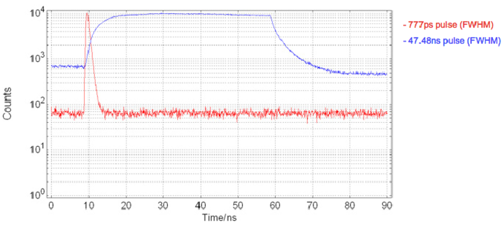
| Shortest Optical Pulse | 777 ps |
| Excitation Wavelength | 450 nm |
| Max. Voltage | 5 V |
| Max. Driver Current | 236 mA (DC) |
| VCO Frequency Range | 7 MHz–800 MHz |
| Setting | Value |
|---|---|
| Laser Rep. Rate | 5 MHz |
| Laser Average Power | 0.15 mW |
| Laser Emission Wavelength | 467 nm |
| Microscope Objective | ×20 |
| SPAD Negative Bias | −19.5 V |
| SPAD Excess Bias | 3.3 V |
| Sample | CdSe/ZnS Quantum Dots |
| Sample Volume | 45 μL |
| Sample Emission Wavelength | 548 nm |
| Concentration | TCSPC Lifetime Value | On-Chip Time-Gated Lifetime Value |
|---|---|---|
| 50 μM | 14.7ns (±114 ps) | 13.7 ns (±122 ps) |
| 25 μM | 14.3 ns (±114 ps) | 13.7 ns (±122 ps) |
| 10 μM | 14.2 ns (±114 ps) | 13.5 ns (±122 ps) |
| 1 μM | 13.3 ns (±114 ps) | 13.8 ns (±122 ps) |
| 0.1 μM | 14.6 ns (±114 ps) | 13.1 ns (±122 ps) |
| 0.01 μM | 10.5 ns (±114 ps) | 13.4 ns (±122 ps) |
© 2009 by the authors; licensee Molecular Diversity Preservation International, Basel, Switzerland. This article is an open access article distributed under the terms and conditions of the Creative Commons Attribution license (http://creativecommons.org/licenses/by/3.0/).
Share and Cite
Rae, B.R.; Muir, K.R.; Gong, Z.; McKendry, J.; Girkin, J.M.; Gu, E.; Renshaw, D.; Dawson, M.D.; Henderson, R.K. A CMOS Time-Resolved Fluorescence Lifetime Analysis Micro-System. Sensors 2009, 9, 9255-9274. https://doi.org/10.3390/s91109255
Rae BR, Muir KR, Gong Z, McKendry J, Girkin JM, Gu E, Renshaw D, Dawson MD, Henderson RK. A CMOS Time-Resolved Fluorescence Lifetime Analysis Micro-System. Sensors. 2009; 9(11):9255-9274. https://doi.org/10.3390/s91109255
Chicago/Turabian StyleRae, Bruce R., Keith R. Muir, Zheng Gong, Jonathan McKendry, John M. Girkin, Erdan Gu, David Renshaw, Martin D. Dawson, and Robert K. Henderson. 2009. "A CMOS Time-Resolved Fluorescence Lifetime Analysis Micro-System" Sensors 9, no. 11: 9255-9274. https://doi.org/10.3390/s91109255