A Micro Oxygen Sensor Based on a Nano Sol-Gel TiO2 Thin Film

Abstract
: An oxygen gas microsensor based on nanostructured sol-gel TiO2 thin films with a buried Pd layer was developed on a silicon substrate. The nanostructured titania thin films for O2 sensors were prepared by the sol-gel process and became anatase after heat treatment. A sandwich TiO2 square board with an area of 350 μm × 350 μm was defined by both wet etching and dry etching processes and the wet one was applied in the final process due to its advantages of easy control for the final structure. A pair of 150 nm Pt micro interdigitated electrodes with 50 nm Ti buffer layer was fabricated on the board by a lift-off process. The sensor chip was tested in a furnace with changing the O2 concentration from 1.0% to 20% by monitoring its electrical resistance. Results showed that after several testing cycles the sensor's output becomes stable, and its sensitivity is 0.054 with deviation 2.65 × 10⁻⁴ and hysteresis is 8.5%. Due to its simple fabrication process, the sensor has potential for application in environmental monitoring, where lower power consumption and small size are required.
1. Introduction
Traditional semiconductor gas sensors for relevant gases like CO, H2, NOx and O2 based on metal oxides have been thoroughly investigated due to their good sensitivity, excellent chemical stability and reversible operation [1]. Titanium dioxide (TiO2) has attracted much attention of researchers since it is a typical metal oxide material which can work in harsh environments such as toxic atmospheres and bad temperature conditions. In the past decade, some reports on TiO2 thick-film sensors were published [2–5]. Meanwhile, attempts were also carried out to develop the TiO2 thin-film sensors. For example, Francioso developed TiO2 thin-film oxygen sensors to control the oxygen concentration in combustion processes in automobile engines in order to replace the traditional zirconium oxide oxygen sensors [6–10]. Thin-film metal oxide semiconductor sensors can be easily integrated with MEMS (Micro-Electro-Mechanical System) micro-hotplates, which results in lower power consumption compared to traditional ones based on thick-film processes.
The preparation of TiO2 thin films with good response properties is a precondition for developing a gas microsensor using such a kind of material. The properties of the films depend on the preparation process and doping method used. The sol-gel method can be used to deposit TiO2 thin films with nano-particles and high specific area. The sensing properties of pure TiO2 thin films are very weak and can be improved by adding doping materials such as Cr, Pt and Nb, etc. To fabricate microsensor-based TiO2 thin films, Francioso and Epifani used the dry etching process [7,10]. However, dry etching tends to change the properties of the deposited TiO2 films, with negative effects on the sol-gel films.
In this paper, a micro O2 sensor which consists of a nano sol-gel TiO2 thin-film board and a pair of interdigitated electrodes was investigated. A wet etching process was applied to define the TiO2 thin-film pattern, and after comparing the quality of the etched board with that fabricated by the dry etching process, wet etching was finally applied in the micro gas sensor fabrication. A pair of micro interdigitated electrodes was fabricated on the board by a lift-off process. X-ray diffraction analysis (XRD) and scanning electron microscopy (SEM) revealed the crystal information and surface topography. Experimental results indicated that the performance of the microsensor is sensitive to O2 with good repeatability. Since the sensor was fabricated on a silicon wafer by the standard micromachining process, it could become an individual device with low power consumption which can be integrated with a micro hotplate in the future and play a useful role in environmental monitoring.
2. Design and Fabrication
2.1. Structure Description
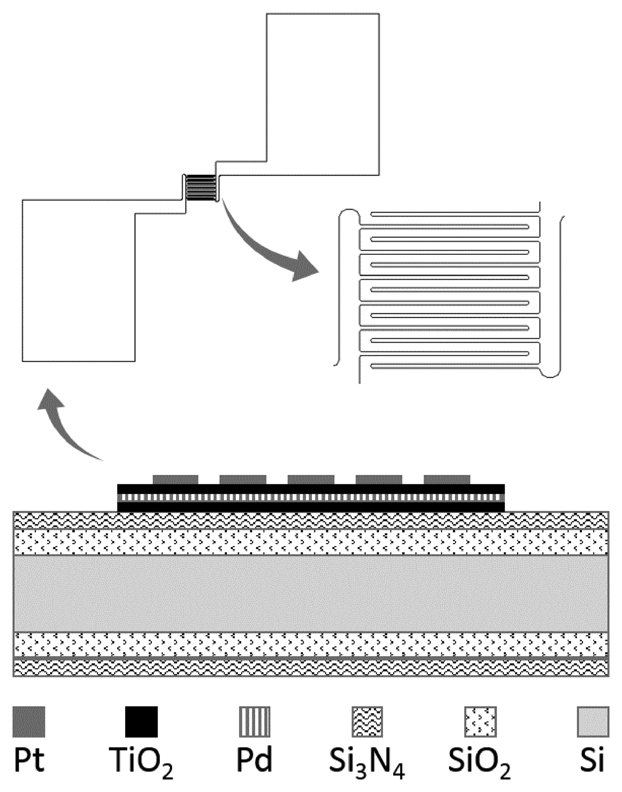
The schematic of the TiO2 oxygen sensor is illustrated in Figure 1. The TiO2 thin film structure was designed as a 350 μm × 350 μm square board, laid out on the surface of a silicon wafer with a deposited SiO2 and Si3N4 layer. On the surface of the TiO2 board, Pt electrodes were designed in an interdigitated pattern. With this design, one can easily fabricate Pt patterning and need not consider the possible influence of the subsequent micromachining process.
The TiO2 film consisted of three layers (TiO2/Pd/TiO2) in a sandwich structure, within which the buried Pd serves as the doping material. More details can be found in our previous work [11]. To simplify the micro gas sensor, in this paper no micro hotplate was integrated.
2.2. Fabrication Process
Fabrication of the micro O2 sensor was completed by a micromachining process, starting from a bare Si substrate. A SiO2 layer (the thickness of the SiO2 film was about 500 nm) was deposited by thermal oxidation and then a Si3N4 layer (150 nm) was deposited by low pressure chemical vapor deposition (LPCVD). To get the sandwich structure, a TiO2 film was formed by a sol-gel process first, and afterward a Pd thin film was deposited by sputtering equipment (Model Explorer 14, Denton Vacuum, Moorestown, NJ, USA). Finally another layer of TiO2 was deposited. Once the TiO2 pattern was defined, the Pt electrodes can be obtained by the lift-off process. During fabrication of the sensor, two steps are important but primary: one is preparation of the nano TiO2 thin film and another is definition of the pattern of the thin film. In the following, we describe them in detail.
Preparation and fabrication of nano TiO2 thin films on a silicon substrate have been reported in some references [12–14]. For a micro gas sensor, the thin film is expected to be a nanostructured material, such as nanoparticles, porous structures, or any other nano-scale form. For this purpose, the sol-gel method was often used to deposit the pure TiO2 thin films [15,16]. One may start by applying spin-coating precursor solution at 2000 rpm onto 4 inch (10.08 cm) oxidized silicon substrates for 30 s, and then the substrate is dried at 80 °C for 30 min and subsequently annealed at 500 °C for 3 h in ambient clean air. With this process, a first layer of TiO2 was successfully deposited with a thickness of 54 nm.
Then the buried Pd layer was deposited on the TiO2 thin film by DC (Direct Current) magnetron sputtering of a pure Pd target using the sputtering system as mentioned above, and then annealed at 500 °C for 2 h. The sputtering time was set to 10 s and its thickness is about 5 nm. Subsequently, the 2nd layer of pure TiO2 thin film, also with thickness of 54 nm, was deposited onto the buried Pd layer with the same process as that of the first one. By this process a sandwich TiO2/Pd/TiO2 thin film, namely, Pd doped TiO2 nanostructured thin film was prepared.
The next step was to define the pattern of the sandwich film. Both wet etching and dry etching were tried to fabricate the pattern. Lithographs for both processes were the same. A layer of positive photoresist (EPG 533) was spun onto the wafer, the rotation rate of the spinner was set to 1500 rpm and the resist thickness about 2 μm was prepared.
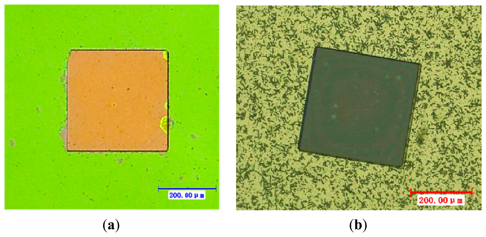
When the wet etching process was used, the sample with the resist pattern was dipped into diluted hydrofluoric acid (HF and H2O with the volume ratio of 1:5). The reaction between HF and titania etched the TiO2 film. After 1 min, the sample's surface was wiped gently with swabs. Then the sample was placed into acetone and cleaned with an ultrasonic washer for 5 min, and thus a square board (350 μm × 350 μm) of thin TiO2 film was patterned on the sample, as shown in Figure 2a.
To find a more reasonable process, dry etching was also investigated to fabricate the square board (350 μm × 350 μm) of titania thin films. This was realized in an ICP (Inductively Coupled Plasma) system (ICP 180, Oxford Instruments, Oxford, UK). The heavy isotropic etching was oriented towards a 100 mTorr chamber pressure when a 40 sccm total flow of SF6, and a 1.5 W/cm2 power RF density were applied to the reactor wafer [7]. The highly controllable process allows a 2 μm resolution sensitive film patterning process. The process lasted for 6 min and the board of titania produced is shown in Figure 2b.
As shown in Figure 2a, the nonfunctional area had been etched more cleanly after wet etching and the square board nano TiO2 film was well shaped. However, for the etched board shown in Figure 2b, many irregular unevennesses may be seen, which may be TiO2 remaining on the nonfunctional area or perhaps the SiO2 layer and Si3N4 layer have been overetched and Si was exposed. In any case, one caneasily see that the wet etching produced a better result.
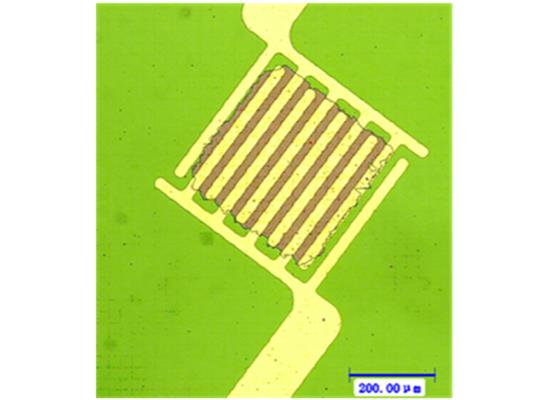
Subsequently, the micro interdigitated electrodes were defined by the UV lithography technology. The 150 nm Pt micro interdigitated electrodes with 50 nm Ti buffer layer were sputtered on the TiO2 thin film board by DC magnetron sputtering and ultrasonic stripping.
As shown in Figure 3, the Pt micro interdigitated electrodes were well-integrated with the sensitive film. The Ti buffer layer and the sensitive film have a better bonding than that of the platinum bonding with sensitive film directly. The photoresist lift-off process was operated gently to avoid fracturing the thin-film edge.
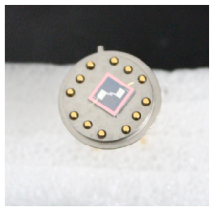
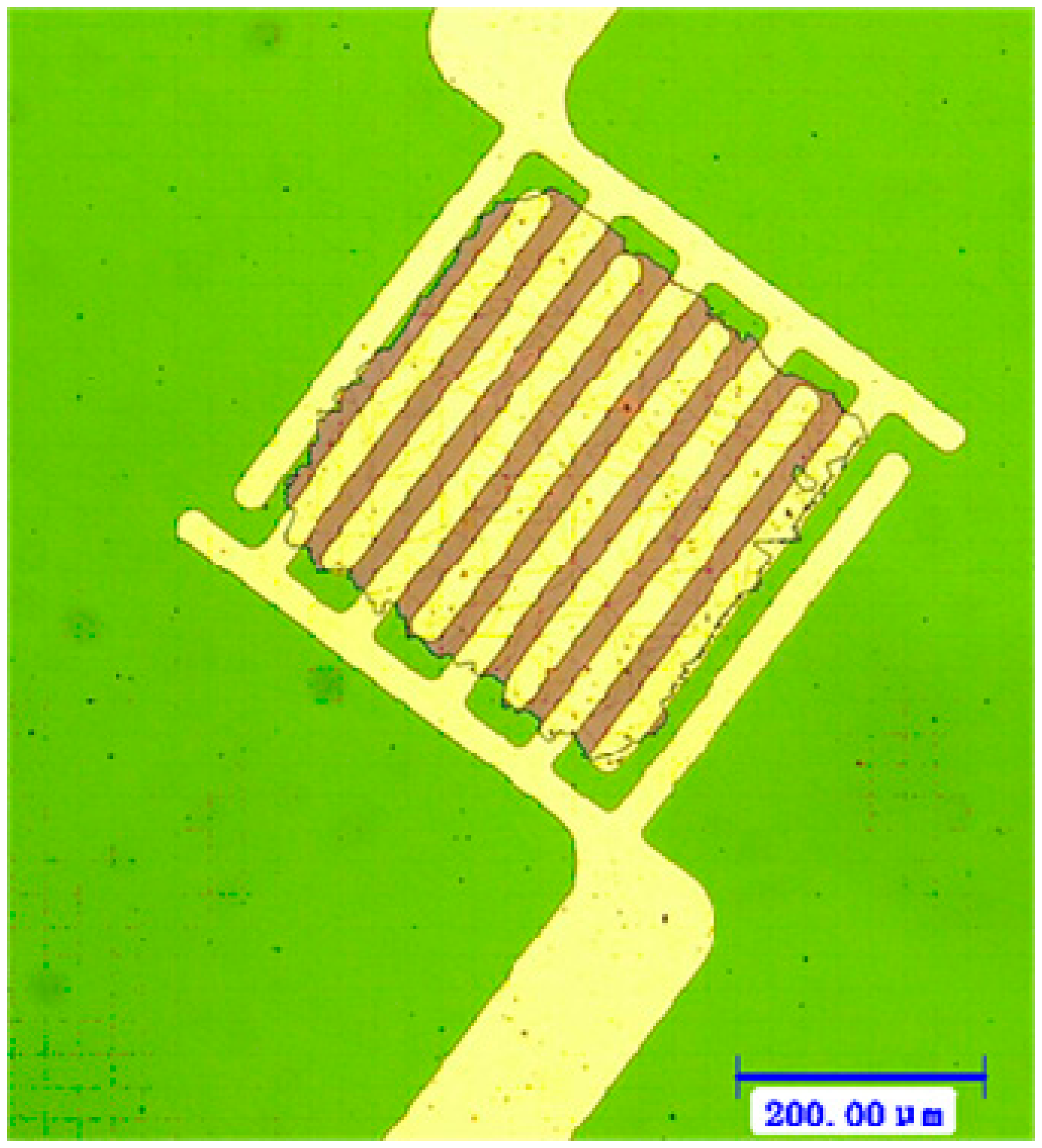
A micro-machined silicon chip (5 mm × 5 mm) was glued on a TO-8 socket as shown in Figure 4. Golden wire bonding was used to make the electrical connections.
The crystalline phases of the pure TiO2 thin films and TiO2/Pd/TiO2 were characterized by X-ray diffraction (XRD, XRD-7000, Shimadzu, Tokyo, Japan) with Cu Kα radiation. Nanostructured pure TiO2 thin films and the doped TiO2 were observed by scanning electron microscope (SEM, Su-8010, Hitachi, Tokyo, Japan).
The electrical response of the samples recorded by a multimeter system (Agilent 34410A, Agilent Technologies, Santa, CA, USA) was carried out in a small chamber heated to 240 °C. The clean air was diluted by dry N2 of 99.999% purity and both gases were controlled with mass flow meters. Subsequently the diluted gas was led into the small chamber. The gas flow rate was kept at 200 sccm.
3. Results and Discussion
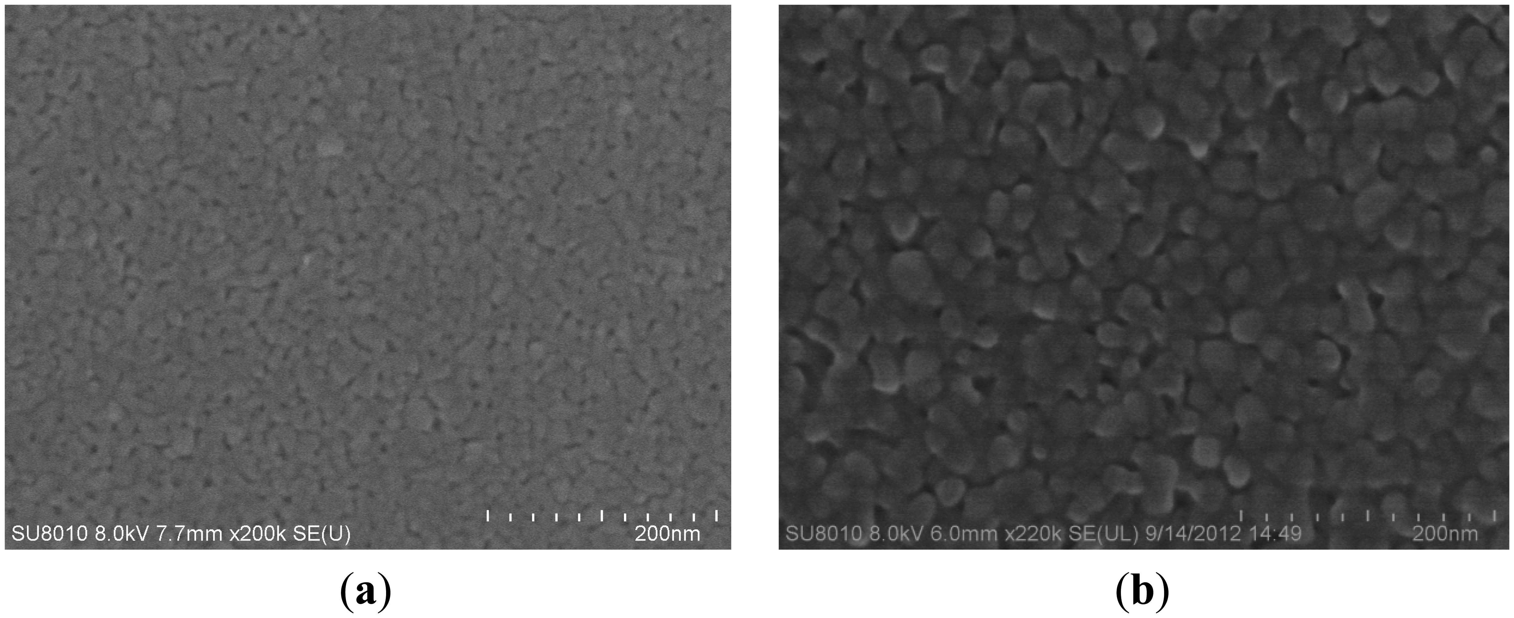
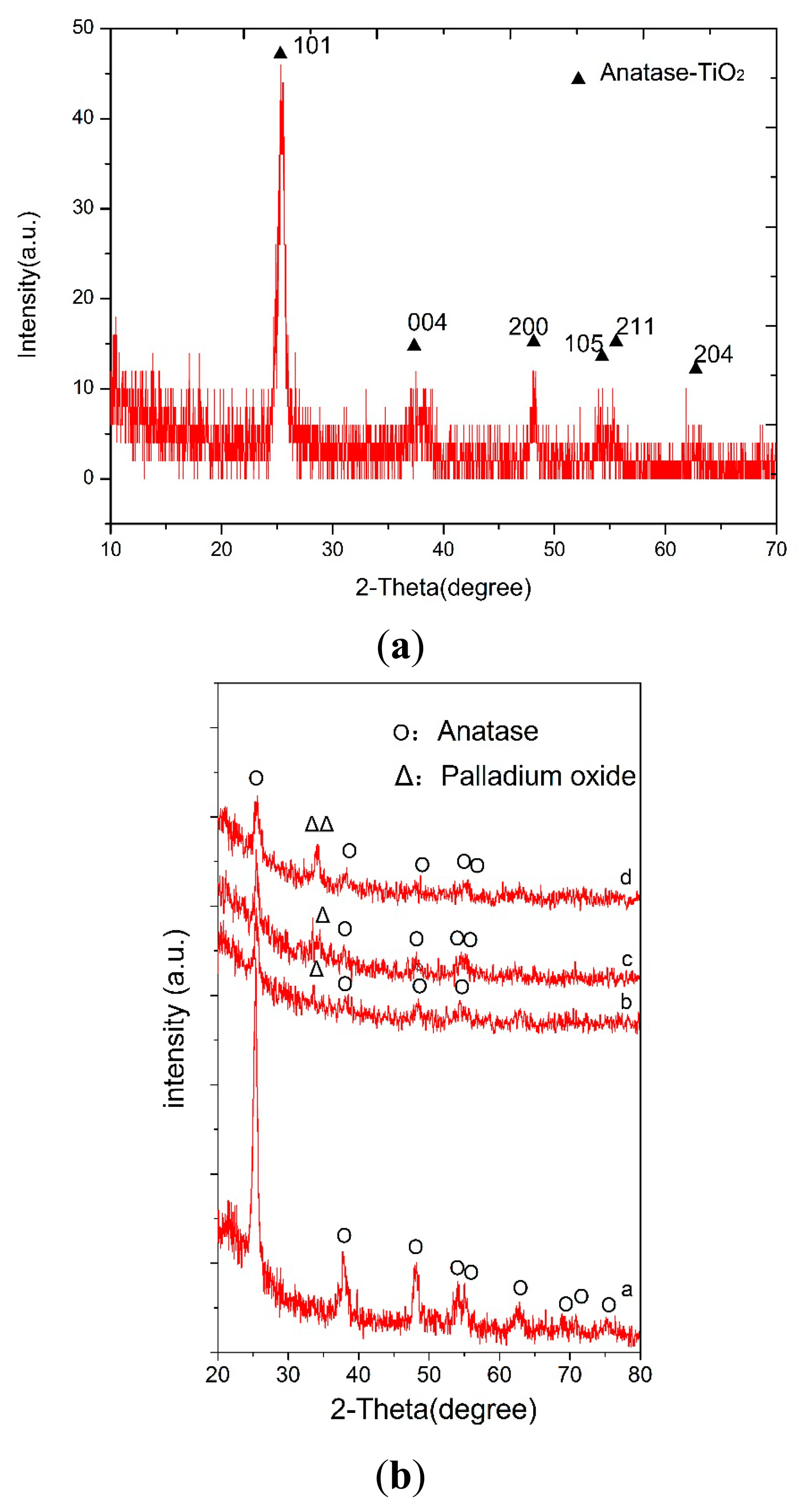
X-ray diffraction (XRD) spectra of the pure TiO2 thin films andTiO2/Pd/TiO2 thin films indicated that the phase of TiO2 is anatase, as shown in Figure 5a and Figure 5b, respectively. However, in the TiO2/Pd/TiO2 thin film, palladium oxide tends to appear, which could enhance the electrical conductivity at low temperature [17,18]. Anatase is usually the desired phase in gas-sensing devices [19,20]. Figure 6a is the SEM image of the TiO2/Pd/TiO2 film, which shows the sensitive film has a highly homogeneous and porous surface with nanoparticles. Compared with the pure TiO2 film as shown in Figure 6b, the TiO2/Pd/TiO2 film has smaller nanoparticle size, higher specific area, and smaller roughness. High homogeneity and small roughness are beneficial to design a micro sensor, since it is not necessary to consider placement and direction of the electrodes when we lay them out on the sensing film.
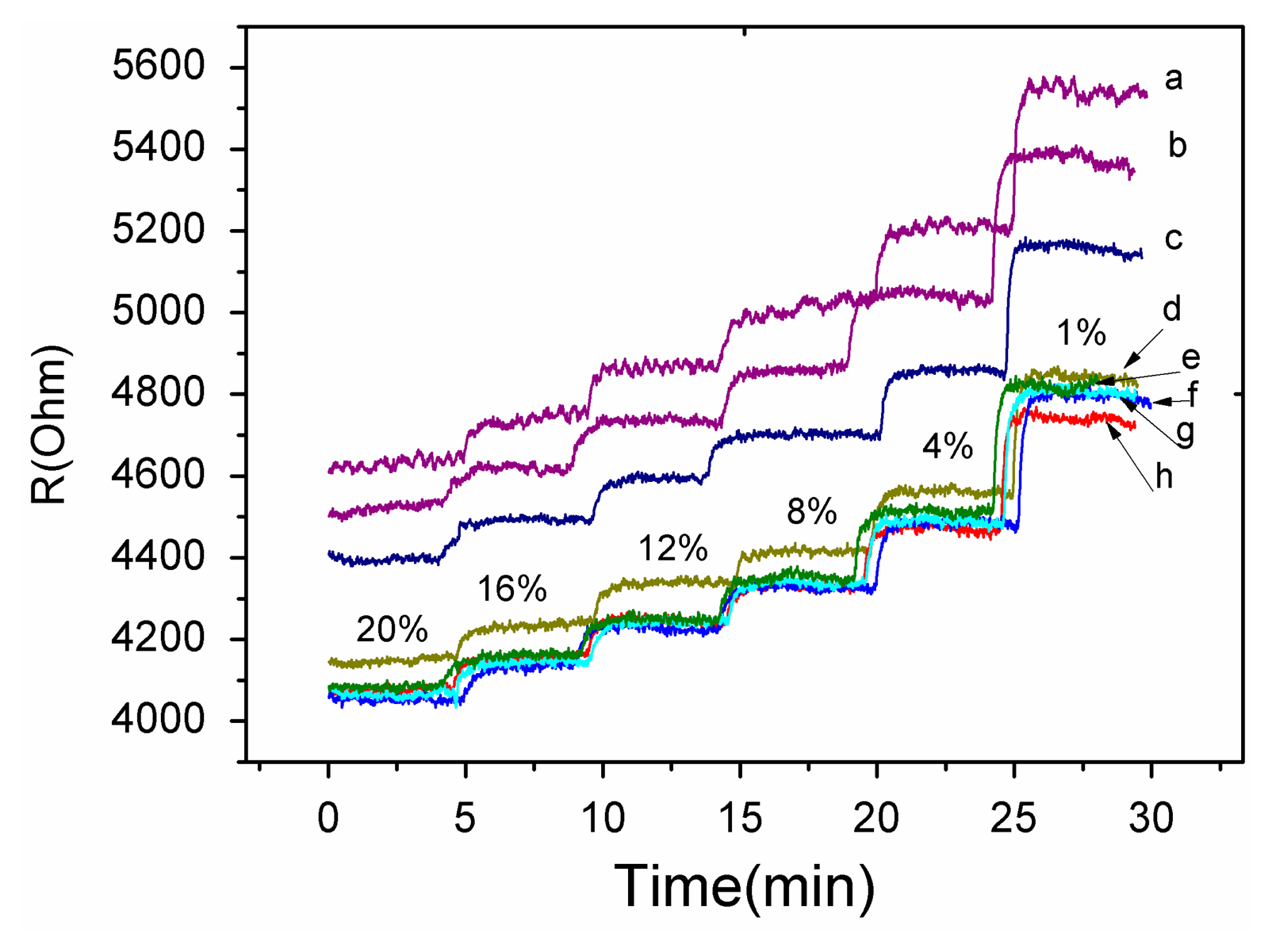
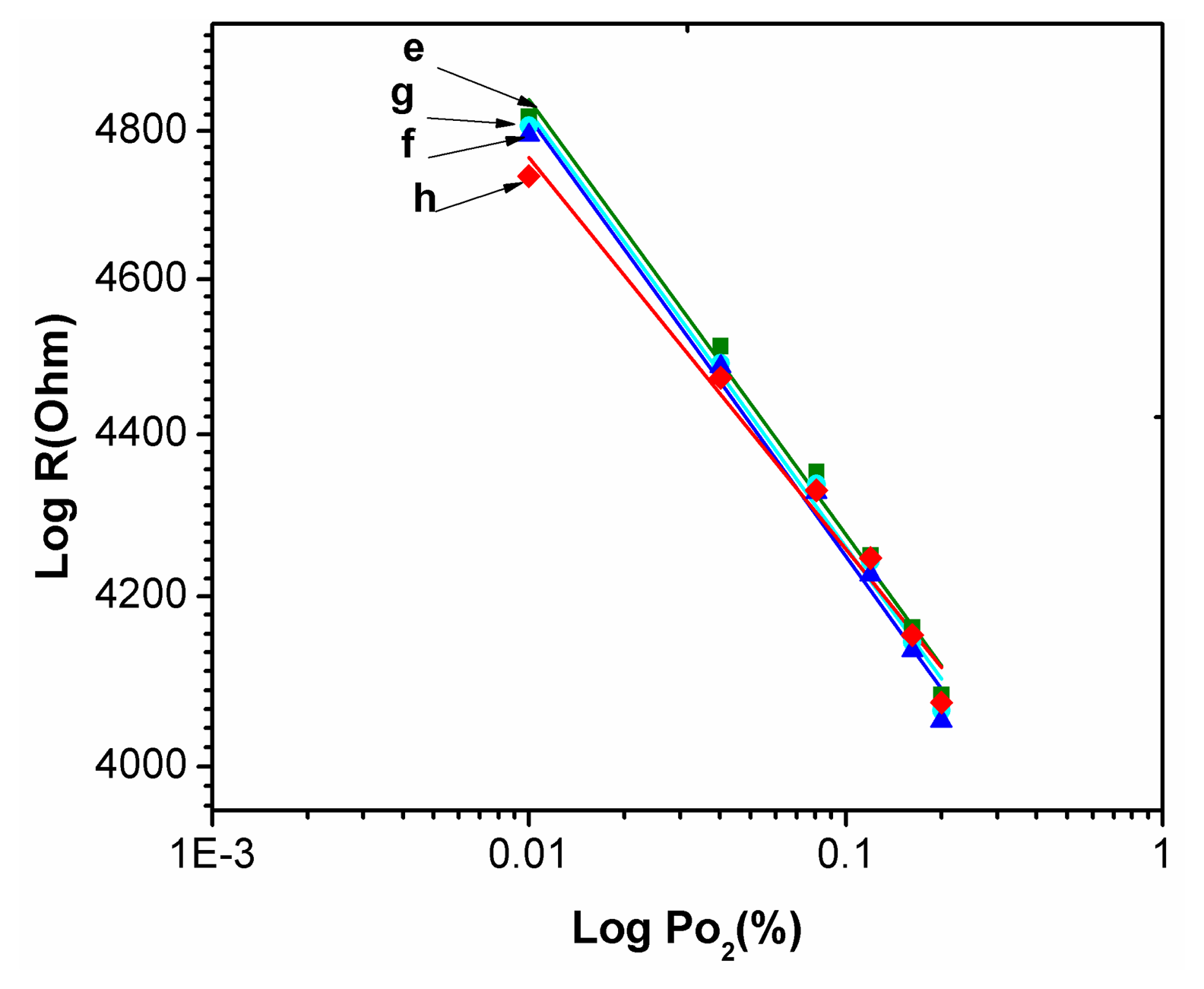
A gas sensing test was carried out to verify the response performance of the microsensor. The structure of TiO2/Pd/TiO2 thin films was tested with 1.0% to 20% oxygen partial pressure at 240 °C. Figure 7 shows the dynamic response and recovery time of the thin films. The sampling interval was set as 1 s and the raw data was plotted in Figure 7. The TiO2 thin films with Pd layer sputtered for 10 s showed good recovery at partial oxygen pressures ranging from 1.0% to 20%. The reproducibility of the different testing cycles of the sensor was tested by several testing process as shown in Figure 6. The test curves e, f, g and h tend to overlap, which indicates the diffusion of Pd has reached a steady state and the sensor based on the TiO2/Pd/TiO2 thin films can output a repeatable signal in different testing cycles.
The decrease of resistance with increasing concentration of O2 in Figure 7, which is indicative of p-type behavior, and the conductivity of the material is governed by holes [21]. However pure TiO2 thin films are a n-type semiconductor material. The diffused Pd layers provide acceptor impurities which can be expressed as:
These impurities make holes the dominant charge carriers in TiO2 thin films. Sinceholes act as the major carriers, O2 adsorption increases number of holes via Reaction (2), which leads to the decreasing resistance with increasing concentration of oxygen seen in Figure 7.
Figure 8 showed the relationship between output resistance R and the input Po2 oxygen partial pressure for the static response of the TiO2 thin film with a buried Pd layer as Po2 varies from 1.0% to 20% at 240 °C. It is can be written as:
The Pd metal ion plays an important role in producing more active oxygen vacancy sites or the incoming oxygen molecules. The concentration of oxygen vacancies will increase as shown in Equation (1). Then the rate of recombination of oxygen vacancies with adsorbed oxygen molecules will be higher. The rate of appearance of holes is also higher. Then the result leads to a large change in the resistivity of the semiconducting oxide and higher sensitivity to oxygen. The fast movement of oxygen vacancies is responsible for a shorter response time [12,15].
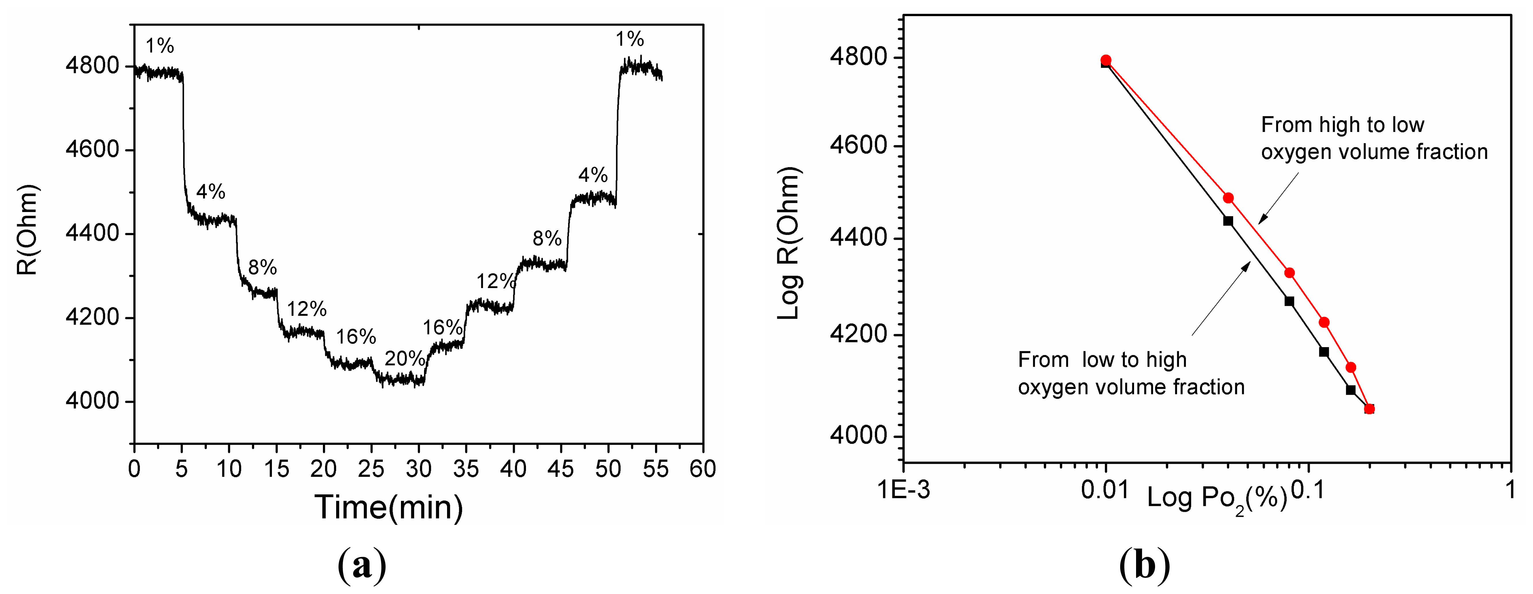
As shown in Figure 9a the sensor output was measured by gradually varying the oxygen partial pressure from 1% to 20% and again from 20% to 1%. Figure 9b shows that when increasing and decreasing the oxygen partial pressure the sensor output differs. The hysteresis is 8.5% and this probably arises from the different rates of adsorption and desorption.
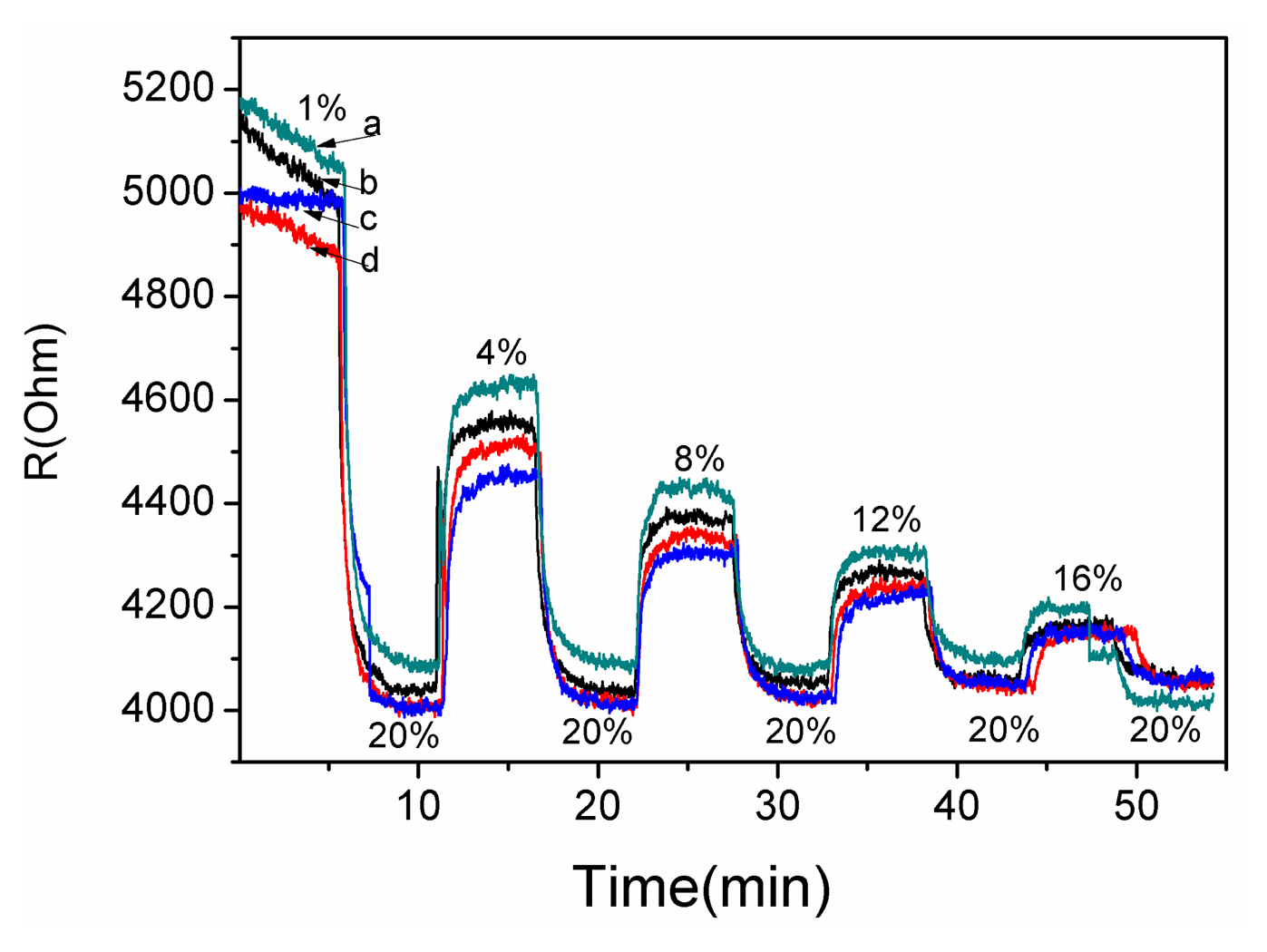
As shown in Figure 10, the average response time of curve d was approximately 52 s and the longest response time was 63 s. Here the response time was defined as the time required to reach 90% of the equilibrium readout. It was measured by switching the gas concentration from 20% and a certain concentration with a time interval 5 min. The micro size of sensitive thin films results in shorter response times than macro-size sensitive thin films [11], since at the micro scale the sensitive thin films can quickly approach gas adsorption equilibrium. The working temperature of the microsensor is 240 °C, which is lower than that reported by the recent literature [22], and the lower temperature is an obvious advantage for lowering the power consumption in real applications.
Selectivity is an important performance features for a gas sensor when there are some interfering gases in the atmosphere. CO2, SO2 and CO which are the main exhaust gases in the fossil fuel combustion process must be taken into account, and response properties of the sensor to these gases will be investigated in the future.
4. Conclusions/Outlook
An oxygen microsensor which uses a pattern of nano sol-gel TiO2 thin film with a buried Pd layer was presented. For the sensor microinterdigitated electrodes were laid out on the top of the TiO2 layer and with this design, the fabrication process was facilitated since wet etching can be applied to make the fabrication process simple and cheap. The response of TiO2 thin films with a buried Pd layer was observed at different oxygen pressures. The result indicates that the n-type of the TiO2 thin films was transformed to p-type behavior by inserting a buried Pd layer. After several cycles, the output signal becomes stable and repeatable. The sensitivity was 0.054 with a deviation of 2.65 × 10⁻⁴, the average response time was 52 s, and the hysteresis was 8.5%. Since the fabrication process is compatible with the MEMS process and it has exhibited good response properties, the proposed micro O2 sensor has potential for practical application. In the future we will focus on a method for integrating the Pd doped TiO2 thin films with a MEMS micro-hotplate to form an actual oxygen sensor.
Acknowledgments
The work is supported by Natural Science Foundation of China (Grants No. 51175416), Major National Science and Technology Projects of China (Grants No. 2013ZX03005007), The Basic Scientific Research Expenses of Central University (Grants No. xjj2014105).
Author Contributions
Hairong Wang proposed the sensor structure and prepared the manuscript. Lei Chen investigated the fabrication process, Jiaxin Wang tested the output properties of the sensor, Quantao Sun and Yulong Zhao provided suggestions on the fabrication process.
Conflicts of Interest
The authors declare no conflict of interest.
References
- Simon, I.; Bârsan, N.; Bauer, M.; Weimar, U. Micromachined metal oxide gas sensors: Opportunities to improve sensor performance. Sens. Actuators B Chem. 2001, 73, 1–26. [Google Scholar]
- Zhang, M.L.; Yuan, Z.H. Fast response of undoped and Li-doped titania thick-films at low temperature. Sens. Actuators B Chem. 2008, 131, 680–686. [Google Scholar]
- Zhuiykov, S.; Wlodarski, W.; Li, Y.X. Nanocrystalline V2O5–TiO2 thin-films for oxygen sensing prepared by sol–gel process. Sens. Actuators B Chem. 2001, 77, 484–490. [Google Scholar]
- Trinchi, A.; Li, Y.X.; Wlodarski, W.; Kaciulis, S.; Pandolfi, L.; Viticoli, S.; Comini, E.; Sberveglieri, G. Investigation of sol–gel prepared CeO2–TiO2 thin films for oxygen gas sensing. Sens. Actuators B Chem. 2003, 95, 145–150. [Google Scholar]
- Sharma, R.K.; Bhatnagar, M.C. Improvement of the oxygen gas sensitivity in doped TiO2 thick films. Sens. Actuators B Chem. 1999, 56, 215–219. [Google Scholar]
- Francioso, L.; Presicce, D.S.; Siciliano, P.; Ficarella, A. Combustion conditions discrimination properties of Pt-doped TiO2 thin film oxygen sensor. Sens. Actuators B Chem. 2007, 123, 516–521. [Google Scholar]
- Francioso, L.; Taurino, A.M.; Forleo, A.; Siciliano, P. TiO2 nanowires array fabrication and gas sensing properties. Sens. Actuators B Chem. 2008, 130, 70–76. [Google Scholar]
- Presicce, D.S.; Francioso, L.; Epifani, M.; Siciliano, P.; Ficarella, A. Temperature and doping effects on performance of titania thin film lambda probe. Sens. Actuators B Chem. 2005, 111, 52–57. [Google Scholar]
- Ga, G.; Mandayo, E.; Castaño, F.J.; Gracia, A.; Cornet, A.; Morante, J.R. Strategies to enhance the carbon monoxide sensitivity of tin oxide thin films. Sens. Actuators B Chem. 2003, 95, 90–96. [Google Scholar]
- Epifani, M.; Helwig, A.; Arbiol, J.; Díaz, R.; Francioso, L.; Siciliano, P.; Mueller, G.; Morante, J.R. TiO2 thin films from titanium butoxide: Synthesis, Pt addition, structural stability, microelectronic processing and gas-sensing properties. Sens. Actuators B Chem. 2008, 130, 599–608. [Google Scholar]
- Wang, H.R.; Sun, Q.T.; Chen, L.; Zhao, Y.L. Sandwich structure of Pd doped nanostructure TiO2 film as O2 sensor. Rev. Sci. Instrum. 2013, 84. org/10.1063/1.4820923. [Google Scholar]
- Sharma, R. K.; Bhatnagar, M.C.; Sharma, G.L. Mechanism of highly sensitive and fast response Cr doped TiO2 oxygen gas sensor. Sens. Actuators B Chem. 1997, 45, 209–215. [Google Scholar]
- Kamata, K.; Maruyama, K.; Amano, S.; Fukazawa, H. Rapid formation of TiO2 films by a conventional CVD method. J. Mater. Sci. Lett. 1990, 9, 316–319. [Google Scholar]
- Yu, J.G.; Yu, H.G.; Cheng, B.; Zhao, X.J.; Yu, J. C.; Ho, W.K. The effect of calcination temperature on the surface microstructure and photocatalytic activity of TiO2 thin films prepared by liquid phase deposition. J. Phys. Chem. B 2003, 107, 13871–13879. [Google Scholar]
- Li, X.G.; Ramasamy, R.; Dutta, P.K. Study of the resistance behavior of anatase and rutile thick films towards carbon monoxide and oxygen at high temperatures and possibilities for sensing applications. Sens. Actuators B Chem. 2009, 143, 308–315. [Google Scholar]
- Atashbar, M.Z.; Sun, H.T.; Gong, B.; Wlodarski, W.; Lcamb, R. XPS study of Nb-doped oxygen sensing TiO2 thin films prepared by sol-gel method. Thin Solid Films 1998, 326, 238–244. [Google Scholar]
- Moon, J.; Park, J.; Lee, S.; Zyung, T.; Kim, I. Pd-doped TiO2 nanofiber networks for gas sensor applications. Sens. Actuators B Chem. 2010, 149, 301–305. [Google Scholar]
- Mardare, D; Iftimie, N.; Crişan, M.; Raileanuc, M.; Yildizd, A.; Comana, T.; Pomonie, K.; Vomvase, A. Electrical conduction mechanism and gas sensing properties of Pd-doped TiO2 films. J. Non Cryst. Solids 2011, 357, 1774–1779. [Google Scholar]
- Gyorgya, E.; Socola, G.; Axentea, E.; Mihailescua, I.N.; Ducub, C.; Ciucac, S. Anatase phase TiO2 thin films obtained by pulsed laser deposition for gas sensing applications. Appl. Surf. Sci. 2005, 247, 429–433. [Google Scholar]
- Ma, X.G.; Tang, C.Q.; Yang, X.H. Effect of relaxation on the energetics and structure of anatase TiO2 (101) surface. Surf. Rev. Lett. 2006, 13, 825–831. [Google Scholar]
- Kim, H.J.; Lee, J.H. Highly sensitive and selective gas sensors using p-type oxide semiconductors: Overview. Sens. Actuators B Chem. 2014, 192, 607–627. [Google Scholar]
- Zhang, M.L.; Ning, T.; Zhang, S.Y.; Li, Z.M.; Yuan, Z.H.; Cao, Q.X. Response time and mechanism of Pd modified TiO2 gas sensor. Mater. Sci. Semicond. Process. 2014, 17, 149–154. [Google Scholar]


© 2014 by the authors; licensee MDPI, Basel, Switzerland. This article is an open access article distributed under the terms and conditions of the Creative Commons Attribution license ( http://creativecommons.org/licenses/by/3.0/).
Share and Cite
Wang, H.; Chen, L.; Wang, J.; Sun, Q.; Zhao, Y. A Micro Oxygen Sensor Based on a Nano Sol-Gel TiO2 Thin Film. Sensors 2014, 14, 16423-16433. https://doi.org/10.3390/s140916423
Wang H, Chen L, Wang J, Sun Q, Zhao Y. A Micro Oxygen Sensor Based on a Nano Sol-Gel TiO2 Thin Film. Sensors. 2014; 14(9):16423-16433. https://doi.org/10.3390/s140916423
Chicago/Turabian StyleWang, Hairong, Lei Chen, Jiaxin Wang, Quantao Sun, and Yulong Zhao. 2014. "A Micro Oxygen Sensor Based on a Nano Sol-Gel TiO2 Thin Film" Sensors 14, no. 9: 16423-16433. https://doi.org/10.3390/s140916423