<?xml version="1.0" encoding="UTF-8"?>
<!DOCTYPE article PUBLIC "-//NLM//DTD Journal Publishing DTD v2.3 20070202//EN" "journalpublishing.dtd">
<article xmlns:mml="http://www.w3.org/1998/Math/MathML" xmlns:xlink="http://www.w3.org/1999/xlink" xml:lang="en" article-type="research-article">
<front>
<journal-meta>
<journal-id journal-id-type="nlm-ta">Sensors</journal-id>
<journal-title>Sensors</journal-title>
<issn pub-type="epub">1424-8220</issn>
<publisher>
<publisher-name>Molecular Diversity Preservation International (MDPI)</publisher-name></publisher></journal-meta>
<article-meta>
<article-id pub-id-type="doi">10.3390/s120505608</article-id>
<article-id pub-id-type="publisher-id">sensors-12-05608</article-id>
<article-categories>
<subj-group>
<subject>Article</subject></subj-group></article-categories>
<title-group>
<article-title>Thermal and Optical Activation Mechanisms of Nanospring-Based Chemiresistors</article-title></title-group>
<contrib-group>
<contrib contrib-type="author">
<name><surname>Dobrokhotov</surname><given-names>Vladimir</given-names></name><xref ref-type="aff" rid="af1-sensors-12-05608"><sup>1</sup></xref><xref ref-type="corresp" rid="c1-sensors-12-05608"><sup>*</sup></xref></contrib>
<contrib contrib-type="author">
<name><surname>Oakes</surname><given-names>Landon</given-names></name><xref ref-type="aff" rid="af1-sensors-12-05608"><sup>1</sup></xref></contrib>
<contrib contrib-type="author">
<name><surname>Sowell</surname><given-names>Dewayne</given-names></name><xref ref-type="aff" rid="af1-sensors-12-05608"><sup>1</sup></xref></contrib>
<contrib contrib-type="author">
<name><surname>Larin</surname><given-names>Alexander</given-names></name><xref ref-type="aff" rid="af1-sensors-12-05608"><sup>1</sup></xref></contrib>
<contrib contrib-type="author">
<name><surname>Hall</surname><given-names>Jessica</given-names></name><xref ref-type="aff" rid="af1-sensors-12-05608"><sup>1</sup></xref></contrib>
<contrib contrib-type="author">
<name><surname>Barzilov</surname><given-names>Alexander</given-names></name><xref ref-type="aff" rid="af1-sensors-12-05608"><sup>1</sup></xref></contrib>
<contrib contrib-type="author">
<name><surname>Kengne</surname><given-names>Alex</given-names></name><xref ref-type="aff" rid="af2-sensors-12-05608"><sup>2</sup></xref></contrib>
<contrib contrib-type="author">
<name><surname>Bakharev</surname><given-names>Pavel</given-names></name><xref ref-type="aff" rid="af2-sensors-12-05608"><sup>2</sup></xref></contrib>
<contrib contrib-type="author">
<name><surname>Corti</surname><given-names>Giancarlo</given-names></name><xref ref-type="aff" rid="af2-sensors-12-05608"><sup>2</sup></xref><xref ref-type="aff" rid="af3-sensors-12-05608"><sup>3</sup></xref></contrib>
<contrib contrib-type="author">
<name><surname>Cantrell</surname><given-names>Timothy</given-names></name><xref ref-type="aff" rid="af3-sensors-12-05608"><sup>3</sup></xref></contrib>
<contrib contrib-type="author">
<name><surname>Prakash</surname><given-names>Tej</given-names></name><xref ref-type="aff" rid="af3-sensors-12-05608"><sup>3</sup></xref></contrib>
<contrib contrib-type="author">
<name><surname>Williams</surname><given-names>Joseph</given-names></name><xref ref-type="aff" rid="af4-sensors-12-05608"><sup>4</sup></xref></contrib>
<contrib contrib-type="author">
<name><surname>Bergman</surname><given-names>Leah</given-names></name><xref ref-type="aff" rid="af2-sensors-12-05608"><sup>2</sup></xref></contrib>
<contrib contrib-type="author">
<name><surname>Huso</surname><given-names>Jesse</given-names></name><xref ref-type="aff" rid="af2-sensors-12-05608"><sup>2</sup></xref></contrib>
<contrib contrib-type="author">
<name><surname>McIlroy</surname><given-names>David</given-names></name><xref ref-type="aff" rid="af2-sensors-12-05608"><sup>2</sup></xref></contrib></contrib-group>
<aff id="af1-sensors-12-05608">
<label>1</label>Department of Physics and Astronomy, Western Kentucky University, Bowling Green, KY 42101, USA; E-Mails: <email>landon.oakes@gmail.com</email> (L.O.); <email>dewayne.sowell363@topper.wku.edu</email> (D.S.); <email>alexander.larin375@topper.wku.edu</email> (A.L.); <email>jessica.hall228@topper.wku.edu</email> (J.H.); <email>alexander.barzilov@wku.edu</email> (A.B.)</aff>
<aff id="af2-sensors-12-05608">
<label>2</label>Department of Physics, E&amp;P Bldg, University of Idaho, Moscow, ID 83844, USA; E-Mails: <email>foue3398@vandals.uidaho.edu</email> (A.K.); <email>bakh8413@vandals.uidaho.edu</email> (P.B.); <email>corti@gonano-9.com</email> (G.C.); <email>lbergman@uidaho.edu</email> (L.B.); <email>huso4579@uidaho.edu</email> (J.H.); <email>dmcilroy@uidaho.edu</email> (D.M.)</aff>
<aff id="af3-sensors-12-05608">
<label>3</label>GoNano Technologies, 112 Sweet Ave., Moscow, ID 83843, USA; E-Mails: <email>Cantrell@gonano-9.com</email> (T.C.); <email>tejasvi.prakash@vandals.uidaho.edu</email> (T.P.)</aff>
<aff id="af4-sensors-12-05608">
<label>4</label>ElectroOptics Research Institute and Nanotechnology Center, University of Louisville, Louisville, KY 40292, USA; E-Mail: <email>jpwill09@louisville.edu</email></aff>
<author-notes>
<corresp id="c1-sensors-12-05608">
<label>*</label>Author to whom correspondence should be addressed; E-Mail: <email>vladimir.dobrokhotov@wku.edu</email>.</corresp></author-notes>
<pub-date pub-type="collection">
<year>2012</year></pub-date>
<pub-date pub-type="epub">
<day>02</day>
<month>05</month>
<year>2012</year></pub-date>
<volume>12</volume>
<issue>5</issue>
<fpage>5608</fpage>
<lpage>5622</lpage>
<history>
<date date-type="received">
<day>13</day>
<month>03</month>
<year>2012</year></date>
<date date-type="rev-recd">
<day>27</day>
<month>03</month>
<year>2012</year></date>
<date date-type="accepted">
<day>12</day>
<month>04</month>
<year>2012</year></date></history>
<permissions>
<copyright-statement>© 2012 by the authors; licensee MDPI, Basel, Switzerland</copyright-statement>
<copyright-year>2012</copyright-year>
<license>
<p>This article is an open access article distributed under the terms and conditions of the Creative Commons Attribution license (http://creativecommons.org/licenses/by/3.0/).</p></license></permissions>
<abstract>
<p>Chemiresistors (conductometric sensor) were fabricated on the basis of novel nanomaterials—silica nanosprings ALD coated with ZnO. The effects of high temperature and UV illumination on the electronic and gas sensing properties of chemiresistors are reported. For the thermally activated chemiresistors, a discrimination mechanism was developed and an integrated sensor-array for simultaneous real-time resistance scans was built. The integrated sensor response was tested using linear discriminant analysis (LDA). The distinguished electronic signatures of various chemical vapors were obtained at ppm level. It was found that the recovery rate at high temperature drastically increases upon UV illumination. The feasibility study of the activation method by UV illumination at room temperature was conducted.</p></abstract>
<kwd-group>
<kwd>nanosprings</kwd>
<kwd>sensor</kwd>
<kwd>electronic nose</kwd></kwd-group></article-meta></front>
<body>
<sec sec-type="intro">
<label>1.</label>
<title>Introduction</title>
<p>Functionalized metal oxides are widely used for vapor sensing applications [<xref ref-type="bibr" rid="b1-sensors-12-05608">1</xref>–<xref ref-type="bibr" rid="b34-sensors-12-05608">34</xref>]. As vapor-sensitive materials they have multiple advantages: high sensitivity, short time of response, and self-refreshability. A productive approach in sensor design is the use of metal oxide-based nanomaterials as the gas sensitive layer. Because of their small size, the internal bulk of the nanomaterials can be very susceptible to changes at their surface due to the fact that the length scales of surface interactions can be comparable to the dimensions of the nanomaterial. For these reasons, nanostructures have been targeted as materials of choice for chemiresistor construction. The sensing mechanism of metal oxide nanostructures is based on the activation of atmospheric oxygen on the surface at high temperatures [<xref ref-type="bibr" rid="b1-sensors-12-05608">1</xref>–<xref ref-type="bibr" rid="b26-sensors-12-05608">26</xref>]. Consequently, the catalytic reactions of gaseous species with oxygen sites on the surface induce charge transfer from the surface to the bulk, which changes the electrical resistance of the device. Despite the multiple attractive features of metal oxides as gas-sensitive materials, the detection of chemicals with a high-temperature chemiresistor can be challenging and presents a number of difficulties, such as: substantial thermal noise, high energy consumption and large size from the incorporation of additional heating elements, temperature controller, and signal processing elements. Also, keeping the device at high temperature reduces its durability. Approaches taken to address these problems require an alternative to the high temperature mechanism of activation. A few successful attempts were taken to utilize an optical activation mechanism by exposing metal oxide films and nanowires to UV radiation [<xref ref-type="bibr" rid="b31-sensors-12-05608">31</xref>–<xref ref-type="bibr" rid="b34-sensors-12-05608">34</xref>]. However, a consistent understanding of UV activation, as well as the comparison of UV <italic>vs.</italic> thermal activation, has yet to be discussed.</p>
<p>In this paper we present the outcomes of a study on a new type of chemiresistor based on ZnO coated silica nanosprings (<xref ref-type="fig" rid="f1-sensors-12-05608">Figure 1(a,b)</xref>). In this chemiresistor, the mat of insulating nanosprings serves as scaffolding for 10–20 nm nanogranular ZnO coatings distributed over the 400 m<sup>2</sup>/g of accessible surface area of nanosprings. This design incorporates the best gas-sensitive properties of nanostructures with the simplicity of thin films: ultra-high surface-to-volume ratio and controllable thickness and morphology of the sensor material. We discuss the effects of UV and thermal activation on the nanospring-based sensor response and compare the magnitudes and times of response, times of reset and other sensor characteristics with the type of activation. On the basis of our measurements and observations, a consistent model of a UV-activated sensor is presented. Also, we demonstrate how exposure of the thermally activated sensor to UV after each cycle of exposure improves the desorption of chemicals from the surface and drastically decreases the time of reset.</p></sec>
<sec>
<label>2.</label>
<title>Material Synthesis and Characterization</title>
<p>Nanospring mats were grown via a vapor-liquid-solid (VLS) mechanism. A detailed description of the process was previously reported by Wang <italic>et al.</italic> [<xref ref-type="bibr" rid="b35-sensors-12-05608">35</xref>] and McIlroy <italic>et al.</italic> [<xref ref-type="bibr" rid="b36-sensors-12-05608">36</xref>]. Nanospring synthesis was performed in a furnace operated at atmospheric pressure. The process uses a gold layer as a catalyst on a Si substrate, which is then exposed to a proprietary silicon precursor [<xref ref-type="bibr" rid="b35-sensors-12-05608">35</xref>–<xref ref-type="bibr" rid="b37-sensors-12-05608">37</xref>] as well as a constant O<sub>2</sub> flow rate concomitant with the silicon precursor. The growth time for an 80 μm thick nanospring-mat is approximately 15 minutes. The nanosprings were coated with ZnO using the ALD technique (<xref ref-type="fig" rid="f1-sensors-12-05608">Figure 1(a,b)</xref>).</p>
<p>ALD utilizes a binary reaction sequence of self-saturating chemical reactions between gaseous precursor molecules and a solid surface to deposit films in a monolayer-by-monolayer fashion [<xref ref-type="bibr" rid="b38-sensors-12-05608">38</xref>,<xref ref-type="bibr" rid="b39-sensors-12-05608">39</xref>]. We argue that ALD coating of silica nanosprings with ZnO has several advantages over self-assembled nanowire mats. Namely, control over the coating thickness and subsequent nanocrystal size and doping is readily achieved. ALD coating of ZnO was carried out in a tube furnace maintained at 170 °C using diethyl zinc and water as the precursors [<xref ref-type="bibr" rid="b39-sensors-12-05608">39</xref>]. Between each pulse of diethyl zinc, or water, the system was purged with N<sub>2</sub>. This ensured that the precursors did not react in the vapor phase and only at the surface of the nanosprings [<xref ref-type="bibr" rid="b40-sensors-12-05608">40</xref>]. At low growth temperatures ZnO films produced by ALD retain their favorable properties, enabling construction of hybrid nanoscale organic/ZnO substrates [<xref ref-type="bibr" rid="b41-sensors-12-05608">41</xref>,<xref ref-type="bibr" rid="b42-sensors-12-05608">42</xref>]. The cycling times are specific to each deposition system, where in this study precursor cycle times were approximately ∼0.25 s or less, and purge and pump times 20–25 s. The thickness of the ZnO layer is controlled by the number of cycles and the purge and precursor pulse widths. Following the above procedure for 200 cycles, a uniformly distributed nanocrystalline ZnO coatings were achieved. Subtle changes in the pump and purge times provides control over the size of the ZnO nanocrystals.</p>
<p>
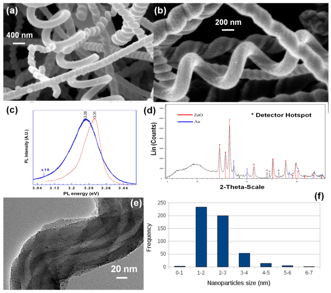
SEM imaging of ZnO/nanosprings shows that the range of average grain sizes is between 3 nm and 100 nm, depending on the ALD conditions. The electronic quality of the ZnO nanocrystals, <italic>i.e.</italic>, the existence of defects, <italic>etc.</italic>, was evaluated by photoluminescence. The photoluminescence (PL) of bare ZnO coated silica nanosprings (ZnO-NS) was analyzed using a CW-Kimmon laser with a wavelength of 325 nm (3.8 eV) together with a JY-Horiba micro-Raman/PL system consisting of a high-resolution T-64000 triple monochromator and a UV microscope capable of focusing to a spot size of ∼800 nm in diameter. Representative room temperature PL spectra of the ZnO coated silica nanosprings (blue) and a single-crystal ZnO reference (red) are displayed in <xref ref-type="fig" rid="f1-sensors-12-05608">Figure 1(c)</xref>. The peak of the PL of the ZnO-NS is ∼50 meV lower in energy than that of the single-crystal ZnO. Our previous study on the PL properties of ZnO nanocrystals and nanostructured flexible ZnO thin films found similar results [<xref ref-type="bibr" rid="b43-sensors-12-05608">43</xref>,<xref ref-type="bibr" rid="b44-sensors-12-05608">44</xref>], where the lower emission was attributed to surface defects. Schirra <italic>et al.</italic> [<xref ref-type="bibr" rid="b45-sensors-12-05608">45</xref>] utilized cathodoluminescence, in conjunction with high resolution imaging, to show that this type of PL originates predominantly from structural defects on ZnO surfaces, such as stacking faults. Furthermore, the broad PL line of the ZnO-NS relative to that of the single crystal is also an indicator of the presence of defects. The crystal structure of the ZnO nanocrystals was verified with X-ray diffraction. Displayed in <xref ref-type="fig" rid="f1-sensors-12-05608">Figure 1(d)</xref> is a representative 2θ-XRD rocking curve for ZnO-NS. The primary peaks of ZnO are all present (red bars), as well as those of Au (blue bars), where Au is the catalyst used for nanospring synthesis. The peaks with * are artifacts of hotspots of the x-ray detector. The XRD spectrum is indicative of good quality ZnO.</p>
<p>In addition to ZnO coated nanosprings, metal nanoparticle-decorated ZnO coated nanosprings were also fabricated (<xref ref-type="fig" rid="f1-sensors-12-05608">Figure 1(e)</xref>). Metal-mediated interactions are expected to increase the sensitivity and selectivity to gases and vapors [<xref ref-type="bibr" rid="b21-sensors-12-05608">21</xref>]. Metal nanoparticles were synthesized on the ZnO coated nanosprings by wet impregnation [<xref ref-type="bibr" rid="b21-sensors-12-05608">21</xref>]. Acetylacetonante (acac)metal-organic salts were dissolved in an organic solvent, such as ethanol or benzene, with a typical base concentration of 1.95 × 10<sup>−2</sup> M of metal content, where the solvent and final concentration varies depending on the material to be deposited. For example, palladium nanoparticles were obtained with a solution of Pd(II) aceylacetonate (Strem Chemicals). For a 1 cm × 1 cm planar sample of nanosprings 10.4 microliters of the solution was applied to the sample surface and the solvent allowed to evaporate at room temperature. Next, the sample was placed in an oven at 500 °C under a hydrogen-nitrogen flow for 15 minutes, thereby reducing the compound to Pd nanoparticles. Finally, the sample was allowed to cool to room temperature in a nitrogen atmosphere to avoid oxidation. The TEM image in <xref ref-type="fig" rid="f1-sensors-12-05608">Figure 1(e)</xref> verifies that this procedure produces a Pd NP size distribution between 2–5 nm, with an average size of 2.4 ± 1.3 nm (<xref ref-type="fig" rid="f1-sensors-12-05608">Figure 1(f)</xref>).</p></sec>
<sec>
<label>3.</label>
<title>Thermal Activation of Chemiresistors</title>
<p>
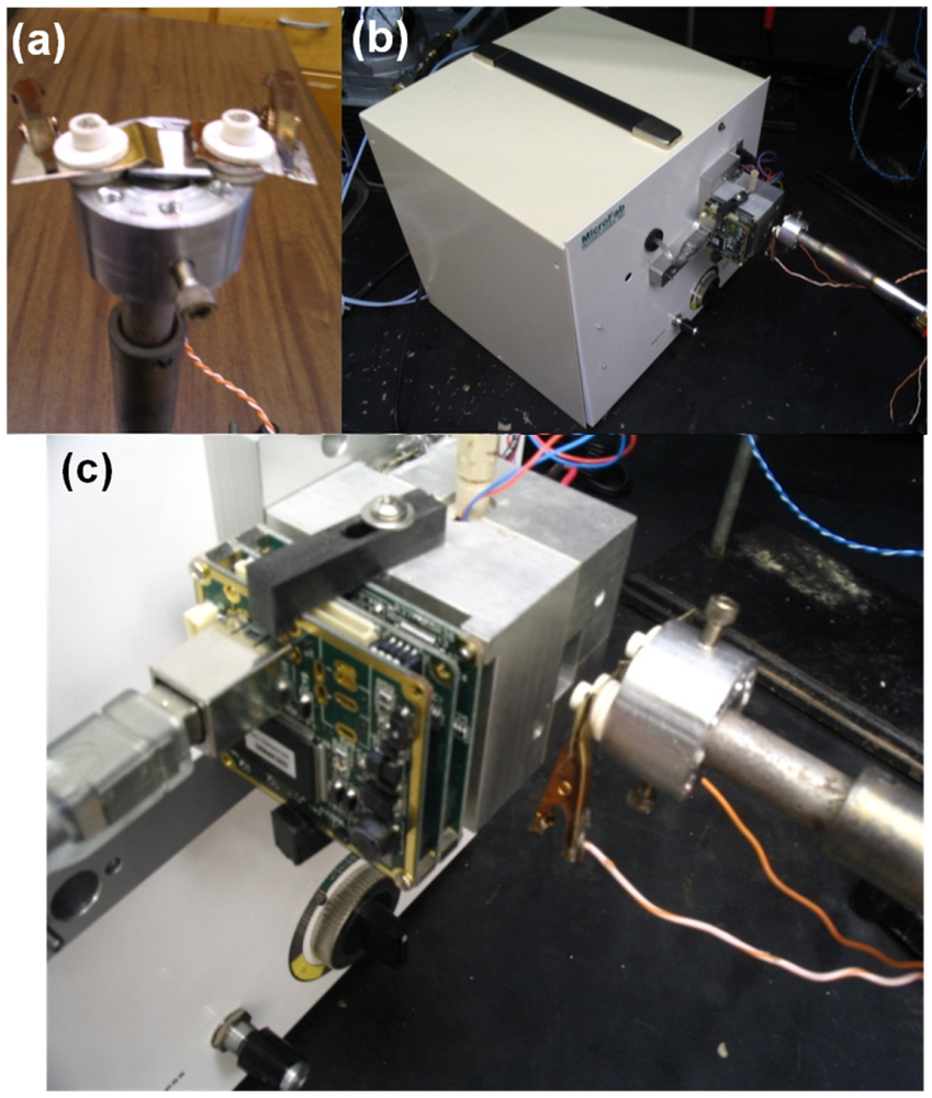
A standard two electrode test geometry was used for measuring the electrical response of the nanospring-based chemiresistors to chemical vapors. The electrodes were annealed and the ohmic nature of ZnO-metal contacts was verified by I-V characterization. The sensor was connected to a thermocouple and placed on a variable temperature platform for temperature control, as shown in the <xref ref-type="fig" rid="f2-sensors-12-05608">Figure 2(a)</xref>. The sensor responses were acquired with a Keithley 2400 SourceMeter interfaced to a computer via Labview-operated data acquisition software allowing for real time conductance measurements. A continuous flow of synthetic air (20% O<sub>2</sub> and 80% N<sub>2</sub>) on the sensor was maintained at all times. The sensor was initially heated to 400 °C in synthetic air at ambient pressure to obtain a steady state resistance. For an average ZnO coating, the resistance upon heating changes from a few kΩ to tens of MΩ. Temperature dependencies of the electronic properties of ZnO-coated nanosprings is significantly different than bulk ZnO. Heating bulk ZnO excites free carriers, producing a drop in resistance. However, for ZnO coated nanosprings, we observed two competing processes: thermal generation of free carriers (decreases the resistance) and trapping of free electrons by ionized oxygen at the surface (increases the resistance). At high temperatures, the depletion by adsorbed oxygen dominates—a necessary condition for high sensitivity. In fact, the ability to adsorb large quantities of oxygen is the most important factor in determining the sensitivity of a chemiresistor, which is based on rapid catalytic reactions.</p>
<p>
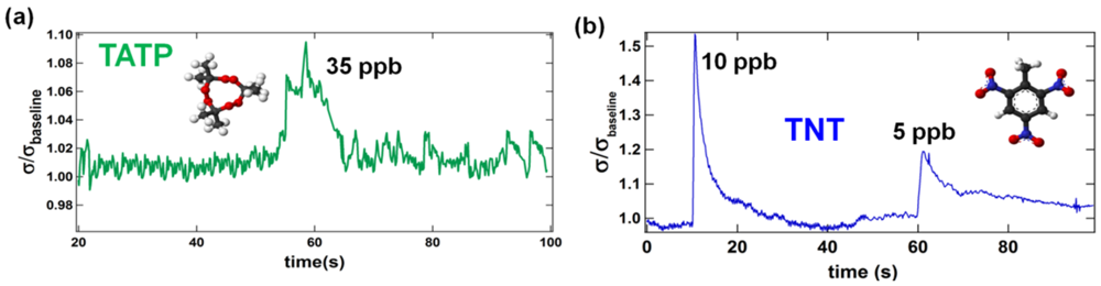
Once a steady state conductance was achieved, pulses of vapor were introduced in the air flow by the VaporJet calibrator [<xref ref-type="bibr" rid="b46-sensors-12-05608">46</xref>], as shown in <xref ref-type="fig" rid="f2-sensors-12-05608">Figure 2(b,c)</xref>. To effectively determine the detection limit of the chemiresistor, sublimation of solids is preferable to the evaporation of liquids. The VaporJet's ability to sublimate solids almost instantly allows for extremely short pulse on the order of milliseconds [<xref ref-type="bibr" rid="b46-sensors-12-05608">46</xref>]. The performance of the Pd/ZnO nanospring sensors was tested using the VaporJet with the explosives trinitrotoluene (TNT) and triacetone triperoxide (TATP) at an operating temperature of 400 °C [<xref ref-type="bibr" rid="b47-sensors-12-05608">47</xref>]. The compounds were introduced into the flow of artificial atmosphere in 0.1 ms pulses. Repeatable peaks of conductance were obtained for both chemicals at ppb levels of concentrations.</p>
<p>Examples of their responses are displayed in <xref ref-type="fig" rid="f3-sensors-12-05608">Figure 3(a,b)</xref>. The results demonstrate that the sensors are extremely sensitive to ppb concentrations and short exposure times. A consequence of these characteristics is their quick recovery of 20–40 s, which demonstrates their superiority to previously reported designs [<xref ref-type="bibr" rid="b1-sensors-12-05608">1</xref>–<xref ref-type="bibr" rid="b34-sensors-12-05608">34</xref>]. Specifically, the best reports on vapor detection of ppb concentrations required several seconds to a few minutes of exposure, <italic>i.e.</italic>, an accumulation of adsorbed vapor onto the sensor's surface was required to achieve a detectable level of response. Examples of their responses are displayed in <xref ref-type="fig" rid="f3-sensors-12-05608">Figure 3(a,b)</xref>. The results demonstrate that the sensors are extremely sensitive to ppb concentrations and short exposure times. A consequence of these characteristics is their quick recovery of 20–40 s, which demonstrates their superiority to previously reported designs [<xref ref-type="bibr" rid="b1-sensors-12-05608">1</xref>–<xref ref-type="bibr" rid="b34-sensors-12-05608">34</xref>]. Specifically, the best reports on vapor detection of ppb concentrations required several seconds to a few minutes of exposure, <italic>i.e.</italic>, an accumulation of adsorbed vapor onto the sensor's surface was required to achieve a detectable level of response. The nearly instantaneous and reversible response of nanospring based sensors to ultra-small vapor concentrations bodes well for their realization as field deployed sensors of explosive. The difference in the detection limit of TNT and TATP (<xref ref-type="fig" rid="f3-sensors-12-05608">Figure 3(a,b)</xref>) is currently attributed to the specific thermodynamic characteristics of the respective catalytic reactions. Contrary to most conventional nitrogen-containing explosives (TNT, PETN, RDX) which transfer much of their energy into heat through rapid catalytic oxidation, peroxide-based explosives, such as TATP, undergo entropic catalytic oxidation resulting in an almost instantaneous decomposition of every solid state TATP molecule into four gas-phase molecules—one ozone and three acetone molecules [<xref ref-type="bibr" rid="b48-sensors-12-05608">48</xref>].</p>
<p>The nearly instantaneous and reversible response of nanospring based sensors to ultra-small vapor concentrations bodes well for their realization as field deployed sensors of explosive. The difference in the detection limit of TNT and TATP (<xref ref-type="fig" rid="f3-sensors-12-05608">Figure 3(a,b)</xref>) is currently attributed to the specific thermodynamic characteristics of the respective catalytic reactions. Contrary to most conventional nitrogen-containing explosives (TNT, PETN, RDX) which transfer much of their energy into heat through rapid catalytic oxidation, peroxide-based explosives, such as TATP, undergo entropic catalytic oxidation resulting in an almost instantaneous decomposition of every solid state TATP molecule into four gas-phase molecules—one ozone and three acetone molecules [<xref ref-type="bibr" rid="b48-sensors-12-05608">48</xref>].</p></sec>
<sec sec-type="methods">
<label>4.</label>
<title>Integrated Sensor Design and Response</title>
<p>
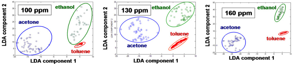
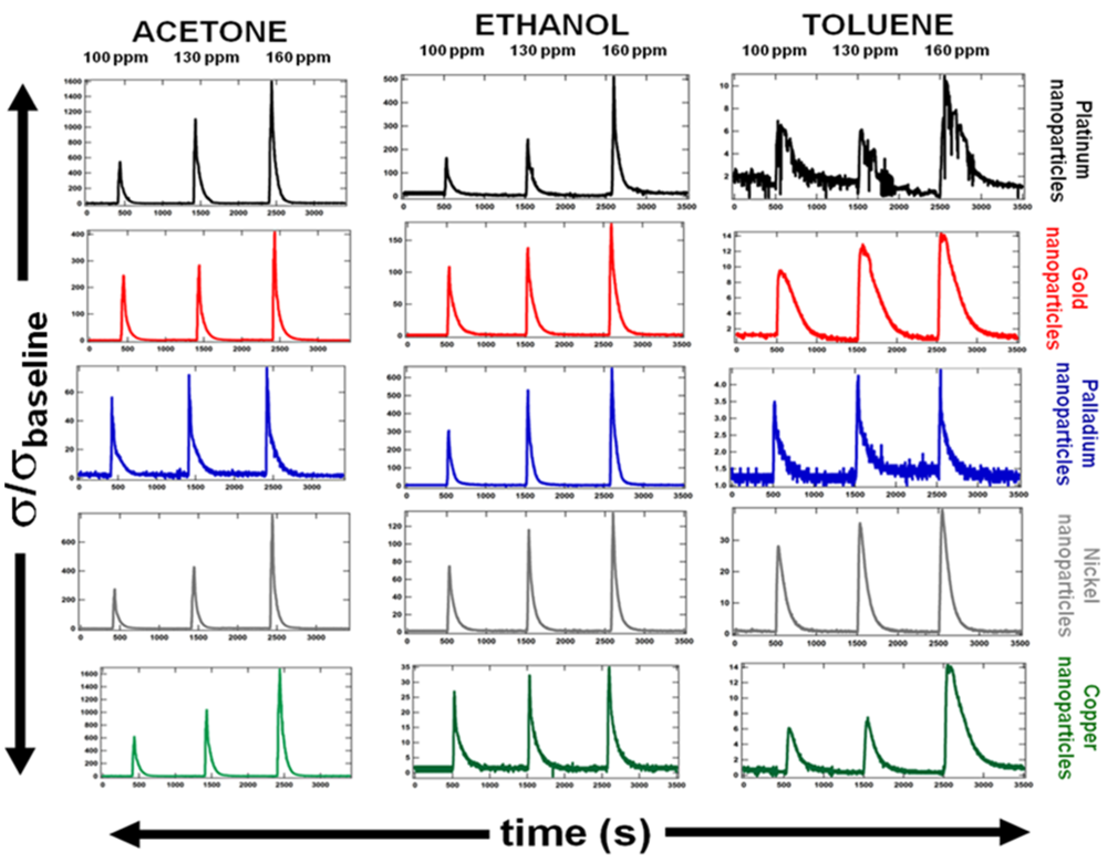
In order to conduct a feasibility study of an artificial olfactory system based on functionalized nanosprings, the simultaneous response of several sensors, coated with the following metal nanoparticles: Pt, Pd, Au, Ni, and Cu, was investigated. To test the electrical response of chemiresistors to chemical vapors, five samples (#1—ZnO/Pt nanoparticles coated, #2—ZnO/Au nanoparticles coated, #3—ZnO/Pd nanoparticles coated, #4—ZnO/Ni nanoparticles coated, and #5—ZnO/Cu nanoparticles coated) were assembled into an integrated array and placed into a tubular flow furnace at 400 °C. Each sensor in the array was connected to Labview-operated data acquisition software through a National Instruments NIcompactDAQ9178 chassis in conjunction with NI9264 voltage source and the NI9203 ammeter, for simultaneous real-time resistance scans. A continuous flow of dry air into the furnace was maintained at all times. Basic degradation products of high-explosives were chosen as analytes for this study. Sequential vapor pulses were introduced into the flow-tube via a VaporJet calibrator. <xref ref-type="fig" rid="f4-sensors-12-05608">Figure 4</xref> summarizes the synchronized matrix of responses of the five sensors to acetone, ethanol and toluene. Each row corresponds to a particular type of sensor, determined by the type of metal nanoparticle coating, while each column corresponds to a particular vapor. Sequential peaks in the graphs correspond to vapor pulses with concentrations of 100 ppm, 130 ppm, and 160 ppm, respectively. The sensor response is measured as conductance normalized to their respective baseline signals in the absence of vapor. Although the chemiresistors are cross-sensitive to multiple gases, the vertical scales drastically differ from graph to graph. For instance, the response of Pd coated ZnO to 160 ppm of acetone is ∼1,500 units, to 160 ppm of ethanol is ∼500 units, and to 160 ppm of toluene is ∼12 units. The relationship between individual sensor responses in the integrated signal appears to be significantly different.</p>
<p>The Linear Discriminant Analysis (LDA) method was used for separation and recognition of vapors. LDA is a commonly used technique for pattern analysis [<xref ref-type="bibr" rid="b1-sensors-12-05608">1</xref>,<xref ref-type="bibr" rid="b49-sensors-12-05608">49</xref>]. It has been widely used and proven successful in many applications. <xref ref-type="fig" rid="f5-sensors-12-05608">Figure 5</xref> demonstrates the LDA analysis of sensor responses shown in the <xref ref-type="fig" rid="f4-sensors-12-05608">Figure 4</xref>. Ten second intervals of the sensor response were used to create transient signals for each of the vapors detected. From these transient signals, common features were extracted to create a feature vector for each sensor. These features include: the signal amplitude, total area beneath the adsorption curve, total area beneath the response curve, and time for the signal to reach its amplitude value [<xref ref-type="bibr" rid="b1-sensors-12-05608">1</xref>,<xref ref-type="bibr" rid="b49-sensors-12-05608">49</xref>]. LDA is used to find a projection which minimizes within class variance while maximizing the distance between class means. This was accomplished by finding a projection which maximizes Fisher's criteria. Responses were then projected onto the Fisher basis vectors to obtain discrimination. The principal components were calculated for three different vapor pressures. As expected, a drop in vapor pressure makes the chemicals less distinguishable (<xref ref-type="fig" rid="f5-sensors-12-05608">Figure 5</xref>). The primary mechanism for increasing the discrimination power of an integrated sensor array is the number of sensors containing different nanoparticles.</p>
<p>To ensure the consistency and reliability of the integrated sensor response, a range of relatively high vapor pressures (between 100 and 200 ppm) and well-known chemical vapors was considered. This selection of vapors was used to conduct a feasibility study of selectivity and specificity of the functionalized nanosprings and to obtain electronic signatures of vapors at different vapor pressures. This selection did not diminish the role of sensitivity and a detection limit of the sensor was obtained along with evidence regarding the ability to recognize more complex chemical vapors. Nanospring-based sensors demonstrate promising capabilities to detect complex vapors such as TNT and TATP at ppb concentrations (<xref ref-type="fig" rid="f3-sensors-12-05608">Figure 3</xref>). However, reliable pattern recognition at this level of signal requires additional pre-processing and noise reduction techniques, which will be left for the future publications.</p></sec>
<sec>
<label>5.</label>
<title>UV Reset Mechanism of Thermally Activated of Chemiresistors</title>
<p>Besides sensitivity and selectivity, the level of noise and baseline stability are important factors in determining overall sensor performance. Baseline stability refers to the ability of a sensor to refresh completely after each cycle of exposure. Due to the fast evaporation of the catalytic reaction products from the ZnO surface, nanospring-based sensors are self-refreshing and, in general, do not need a reset mechanism. For gases like CO, where the oxidation to CO<sub>2</sub> is a simple one-step catalytic reaction, the recovery rate is faster compared with vapors and the recovery curve is more smooth [<xref ref-type="bibr" rid="b3-sensors-12-05608">3</xref>–<xref ref-type="bibr" rid="b26-sensors-12-05608">26</xref>]. Upon exposure to simple vapors such as toluene or ethanol the recovery time is longer; however, the recovery persists for a few seconds with complete baseline restoration [<xref ref-type="bibr" rid="b3-sensors-12-05608">3</xref>–<xref ref-type="bibr" rid="b26-sensors-12-05608">26</xref>]. For complex organic analytes (TNT, TATP, RDX, HMX) with several intermediate oxidation stages, it is highly desirable to reduce the recovery time in order to achieve proper efficiency and accuracy. For example, TNT (C<sub>7</sub>H<sub>5</sub>N<sub>3</sub>O<sub>6</sub>) is able to undergo full catalytic oxidation with products of carbon dioxide, water and nitrogen gas. However, TNT has a negative oxygen balance, which implies that the oxygen content of the molecule is insufficient compared to the amount of oxygen needed to form all of these products. Thus, as with many explosives, TNT's oxidation is more efficient in the presence of an external oxidant, implying that the oxygen-rich high-temperature surface of ZnO comprises an environment favorable for the following catalytic reaction:
<disp-formula id="FD1">
<label>(1)</label>
<mml:math id="mm1" display="block">
<mml:semantics id="sm1">
<mml:mrow>
<mml:mn>2</mml:mn>
<mml:msub>
<mml:mi>C</mml:mi>
<mml:mn>7</mml:mn></mml:msub>
<mml:msub>
<mml:mi>H</mml:mi>
<mml:mn>5</mml:mn></mml:msub>
<mml:msub>
<mml:mi>N</mml:mi>
<mml:mn>3</mml:mn></mml:msub>
<mml:msub>
<mml:mi>O</mml:mi>
<mml:mn>6</mml:mn></mml:msub>
<mml:mo>+</mml:mo>
<mml:mn>21</mml:mn>
<mml:msup>
<mml:mi>O</mml:mi>
<mml:mo>−</mml:mo></mml:msup>
<mml:mo>→</mml:mo>
<mml:mn>14</mml:mn>
<mml:mi>C</mml:mi>
<mml:msub>
<mml:mi>O</mml:mi>
<mml:mn>2</mml:mn></mml:msub>
<mml:mo>+</mml:mo>
<mml:mn>5</mml:mn>
<mml:msub>
<mml:mi>H</mml:mi>
<mml:mn>2</mml:mn></mml:msub>
<mml:mi>O</mml:mi>
<mml:mo>+</mml:mo>
<mml:mn>3</mml:mn>
<mml:msub>
<mml:mi>N</mml:mi>
<mml:mn>2</mml:mn></mml:msub>
<mml:mo>+</mml:mo>
<mml:mn>21</mml:mn>
<mml:msup>
<mml:mi>e</mml:mi>
<mml:mo>−</mml:mo></mml:msup></mml:mrow></mml:semantics></mml:math></disp-formula></p>
<p>During this reaction, some of the TNT molecules experience only partial oxidation upon reaching the ZnO surface. The intermediate reaction products (dinitrotoluene, toluene <italic>etc.</italic>) remain attached to surface defects and then oxidize at a slower rate to the final oxidation stage gaseous products. These products evaporate from the surface, causing re-adsorption of atmospheric oxygen and thus baseline restoration. The average thermal energy of electrons in bulk ZnO may not be high enough to ionize atmospheric oxygen into <italic>O</italic><sup>–</sup> groups on the surface. Only a small fraction of high-energy electrons are involved in the oxygen ionization, creating a slow recovery rate. These processes together cause the step-like behavior observed in the desorption portion of the vapor-sensing characteristics (<xref ref-type="fig" rid="f6-sensors-12-05608">Figure 6(a)</xref>) which is often erroneously attributed to thermal noise despite the amplitude of these steps being sufficiently higher than the noise. This step-like behavior is not observed in the sensing characteristics of simple gases, where the full catalytic oxidation occurs in a single-step. For instance, carbon monoxide oxidizes to carbon dioxide via the following reaction:
<disp-formula id="FD2">
<label>(2)</label>
<mml:math id="mm2" display="block">
<mml:semantics id="sm2">
<mml:mrow>
<mml:mtext mathvariant="italic">CO</mml:mtext>
<mml:mo>+</mml:mo>
<mml:msup>
<mml:mi>O</mml:mi>
<mml:mo>−</mml:mo></mml:msup>
<mml:mo>→</mml:mo>
<mml:mi>C</mml:mi>
<mml:msub>
<mml:mi>O</mml:mi>
<mml:mn>2</mml:mn></mml:msub>
<mml:mo>+</mml:mo>
<mml:msup>
<mml:mi>e</mml:mi>
<mml:mo>−</mml:mo></mml:msup></mml:mrow></mml:semantics></mml:math></disp-formula></p>
<p>
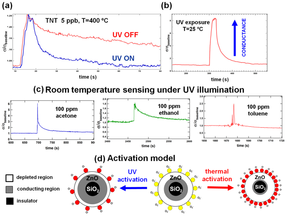
To increase the sensor recovery rate after a TNT pulse, the nanospring-mat was exposed to broad-spectrum UV radiation. ZnO is well known for its high optical activity [<xref ref-type="bibr" rid="b31-sensors-12-05608">31</xref>–<xref ref-type="bibr" rid="b34-sensors-12-05608">34</xref>]; therefore, when this wide band gap material (band gap 3.4 eV) is illuminated under UV light with energy equal or greater than 3.4 eV, a large number of high-energy electron-hole pairs (excitons) is generated. In addition, the products of partial TNT oxidation can be cracked by UV light and oxidized by the activated oxygen on the surface. Once the gaseous products of full oxidation (CO<sub>2</sub>, H<sub>2</sub>O, and N<sub>2</sub>) desorb from ZnO, the high energy electrons generated by UV light ionize the atmospheric oxygen on the surface and restore <italic>O</italic><sup>−</sup> coverage. The experimental observation of this effect is shown in the <xref ref-type="fig" rid="f6-sensors-12-05608">Figure 6(a)</xref>, where the recovery rate at high temperature drastically increases upon the UV illumination.</p></sec>
<sec>
<label>6.</label>
<title>Room Temperature UV Activation of Chemiresistors</title>
<p>At room temperature, the exposure of nanosprings to UV light in the ambient air causes an increase in conductance by a factor of eight (<xref ref-type="fig" rid="f6-sensors-12-05608">Figure 6(b)</xref>). This jump in conductance is attributed to the enhanced carrier density in the nanospring and the reduced depletion width. Once the electron-hole pairs are generated by the UV light, the holes migrate to the surface and discharge the adsorbed oxygen ions. This causes the depletion layer width and the intergranule barrier height to decrease, resulting in the desorption of surface oxygen. Over time, the unpaired electrons accumulate until the desorption and adsorption of oxygen reaches an equilibrium state. Hence, UV excitation leads to an enhanced carrier density in the nanospring and a narrower depletion width, resulting in a gradual increase in current until saturation.</p>
<p>The UV-activated room-temperature gas sensing characteristics for the ZnO/Pd coated sensor upon exposure to a 1 sec pulse of vapor phase analytes at 100 ppm are shown in the <xref ref-type="fig" rid="f6-sensors-12-05608">Figure 6(c)</xref>. The UV-activated sensor responds to a vapor pulse and returns to the steady state faster than if it were thermally activated and does so with a significantly lower level of noise. However, the response level of the UV-activated sensor is more than ten times lower than the response of a thermally activated one. The measurable response to ppb levels of TNT and TATP at room temperature was not observed. Although the sensing mechanism for thermally-activated ZnO and UV-activated ZnO are the same, the steady state conditions for them are qualitatively different. For the thermally-activated sensor, a significant increase in resistance in the steady state due to the depletion of ZnO by the adsorbed oxygen is an indicator of high sensitivity. In contrast, for a UV-activated sensor in the steady state under constant UV illumination the resistance drops, indicating that the amount of adsorbed oxygen is less than for the non-UV room temperature conditions. Although it seems like a paradox, the mechanism of this effect is hidden in the nature of the adsorbed oxygen species. The mechanism of UV-activation of a ZnO sensor is shown in the <xref ref-type="fig" rid="f6-sensors-12-05608">Figure 6(d)</xref>. Under non-UV conditions ionized oxygen chemisorbs on the surface in its molecular form, <italic>O</italic><sub>2</sub><sup>−</sup>. In this form it is less interactive: analogously, the sensitivity of high-temperature sensors is very low below 150 °C, when the molecular form prevails. When UV exposed ZnO reaches the steady-state adsorption-desorption equilibrium, the amount of adsorbed oxygen decreases compared to non-UV conditions. However, the presence of high energy excitons leads to the formation of the atomic form of adsorbed oxygen, <italic>O</italic><sup>−</sup>, which is substantially more chemically interactive and creates favorable conditions for catalytic reactions.</p></sec>
<sec sec-type="conclusions">
<label>7.</label>
<title>Conclusions</title>
<p>We have developed a method for constructing high surface area chemiresistors using silica nanosprings as scaffolding. The chemiresistors were fabricated by coating the silica nanosprings by atomic layer deposition with ZnO, or ZnO followed by decoration with Pd nanoparticles. Thermal and optical methods of sensor activation were developed and compared. At 400 °C, well-defined spikes in conductance upon exposure to explosive vapors (TNT, TATP) were obtained for 0.1 ms exposure times at ppb levels. It was found that exposure of the thermally activated sensor to UV light after each cycle of exposure improves the desorption of chemicals from the surface and drastically decreases the time of reset. Room temperature UV-activation of solid state sensors has multiple attractive features, such as: sufficient noise reduction, stable baseline, short time of response and recovery, long durability and low energy consumption. However, the detection limit is sufficiently higher for the thermally activated sensors. Therefore, until the UV mechanism is fully developed, thermal excitation remains the primary mechanism for activation in oxide-based chemical sensors.</p></sec></body>
<back>
<ack>
<p>Authors would like to thank the Office of Naval Research (grant # N00014-10-1-0282) for the support of this work. DMc would like to acknowledge the USDA and the Dyess Faculty Fellowship for additional support.</p></ack>
<ref-list>
<title>References</title>
<ref id="b1-sensors-12-05608"><label>1.</label><citation citation-type="book"><source>Handbook of Machine Olfaction: Electronic Nose Technology</source><person-group person-group-type="editor"><name><surname>Pearce</surname><given-names>T.C.</given-names></name><name><surname>Schiffman</surname><given-names>S.S.</given-names></name><name><surname>Nagle</surname><given-names>H.T.</given-names></name><name><surname>Gardner</surname><given-names>J.W.</given-names></name></person-group><publisher-name>John Wiley &amp; Sons</publisher-name><publisher-loc>Hoboken, NJ, USA</publisher-loc><fpage>2003</fpage></citation></ref>
<ref id="b2-sensors-12-05608"><label>2.</label><citation citation-type="journal"><person-group person-group-type="author"><name><surname>Yinon</surname><given-names>J.</given-names></name></person-group><article-title>Detection of explosives by electronic noses</article-title><source>Anal. Chem.</source><year>2003</year><volume>75</volume><fpage>98A</fpage><lpage>105A</lpage><pub-id pub-id-type="doi">10.1021/ac020428b</pub-id></citation></ref>
<ref id="b3-sensors-12-05608"><label>3.</label><citation citation-type="journal"><person-group person-group-type="author"><name><surname>Kolmakov</surname><given-names>A.</given-names></name><name><surname>Klenov</surname><given-names>D.O.</given-names></name><name><surname>Lilach</surname><given-names>Y.</given-names></name><name><surname>Stemmer</surname><given-names>S.</given-names></name><name><surname>Moskovits</surname><given-names>M.</given-names></name></person-group><article-title>Enhanced gas sensing by individual SnO<sub>2</sub> nanowires and nanobelts functionalized with Pd catalyst particles</article-title><source>Nano Lett.</source><year>2005</year><volume>5</volume><fpage>667</fpage><lpage>673</lpage><pub-id pub-id-type="doi">10.1021/nl050082v</pub-id><pub-id pub-id-type="pmid">15826106</pub-id></citation></ref>
<ref id="b4-sensors-12-05608"><label>4.</label><citation citation-type="journal"><person-group person-group-type="author"><name><surname>Sysoev</surname><given-names>V.V.</given-names></name><name><surname>Goschnick</surname><given-names>J.</given-names></name><name><surname>Schneider</surname><given-names>T.</given-names></name><name><surname>Strelcov</surname><given-names>E.</given-names></name><name><surname>Kolmakov</surname><given-names>A.</given-names></name></person-group><article-title>A gradient microarray electronic nose based on percolating SnO<sub>2</sub> nanowire sensing elements</article-title><source>Nano Lett.</source><year>2007</year><volume>7</volume><fpage>3182</fpage><lpage>3188</lpage><pub-id pub-id-type="doi">10.1021/nl071815+</pub-id><pub-id pub-id-type="pmid">17924710</pub-id></citation></ref>
<ref id="b5-sensors-12-05608"><label>5.</label><citation citation-type="journal"><person-group person-group-type="author"><name><surname>Sysoev</surname><given-names>V.V.</given-names></name><name><surname>Kiselev</surname><given-names>I.</given-names></name><name><surname>Frietsch</surname><given-names>M.</given-names></name><name><surname>Goschnick</surname><given-names>J.</given-names></name></person-group><article-title>Temperature gradient effect on gas discrimination power of a metal-oxide thin-film sensor microarray</article-title><source>Sensors</source><year>2004</year><volume>4</volume><fpage>37</fpage><lpage>46</lpage><pub-id pub-id-type="doi">10.3390/s40400037</pub-id></citation></ref>
<ref id="b6-sensors-12-05608"><label>6.</label><citation citation-type="journal"><person-group person-group-type="author"><name><surname>Sysoev</surname><given-names>V.V.</given-names></name><name><surname>Button</surname><given-names>B.K.</given-names></name><name><surname>Wepsiec</surname><given-names>K.</given-names></name><name><surname>Dmitriev</surname><given-names>S.</given-names></name><name><surname>Kolmakov</surname><given-names>A.</given-names></name></person-group><article-title>Towards the nanoscopic “electronic nose”: Hydrogen <italic>versus</italic> carbon monoxide discrimination with an array of individual metal oxide nano- and meso-wire sensors</article-title><source>Nano Lett.</source><year>2006</year><volume>6</volume><fpage>1584</fpage><lpage>1588</lpage><pub-id pub-id-type="doi">10.1021/nl060185t</pub-id><pub-id pub-id-type="pmid">16895339</pub-id></citation></ref>
<ref id="b7-sensors-12-05608"><label>7.</label><citation citation-type="journal"><person-group person-group-type="author"><name><surname>Barsan</surname><given-names>N.</given-names></name><name><surname>Weimar</surname><given-names>U.</given-names></name></person-group><article-title>Conduction model of metal oxide gas sensors</article-title><source>J. Electroceramics</source><year>2001</year><volume>7</volume><fpage>143</fpage><lpage>167</lpage><pub-id pub-id-type="doi">10.1023/A:1014405811371</pub-id></citation></ref>
<ref id="b8-sensors-12-05608"><label>8.</label><citation citation-type="journal"><person-group person-group-type="author"><name><surname>Barsan</surname><given-names>N.</given-names></name><name><surname>Weimar</surname><given-names>U.</given-names></name></person-group><article-title>Understanding the fundamental principles of metal oxide based gas sensors; the example of CO sensing with SnO<sub>2</sub> sensors in the presence of humidity</article-title><source>J. Phys. Condens. Matter</source><year>2003</year><volume>15</volume><fpage>R813</fpage><lpage>R839</lpage><pub-id pub-id-type="doi">10.1088/0953-8984/15/20/201</pub-id></citation></ref>
<ref id="b9-sensors-12-05608"><label>9.</label><citation citation-type="journal"><person-group person-group-type="author"><name><surname>Gurlo</surname><given-names>A.</given-names></name><name><surname>Bârsan</surname><given-names>N.</given-names></name><name><surname>Oprea</surname><given-names>A.</given-names></name><name><surname>Sahm</surname><given-names>M.</given-names></name><name><surname>Sahm</surname><given-names>T.</given-names></name><name><surname>Weimar</surname><given-names>U.</given-names></name></person-group><article-title>An n- to p-type conductivity transition induced by oxygen adsorption on a-Fe<sub>2</sub>O<sub>3</sub></article-title><source>Appl. Phys. Lett.</source><year>2004</year><volume>85</volume><pub-id pub-id-type="doi">10.1063/1.1794853.</pub-id></citation></ref>
<ref id="b10-sensors-12-05608"><label>10.</label><citation citation-type="journal"><person-group person-group-type="author"><name><surname>Capone</surname><given-names>S.</given-names></name><name><surname>Forleo</surname><given-names>A.</given-names></name><name><surname>Francioso</surname><given-names>L.</given-names></name><name><surname>Rella</surname><given-names>R.</given-names></name><name><surname>Siciliano</surname><given-names>P.</given-names></name><name><surname>Spadavecchia</surname><given-names>J.</given-names></name><name><surname>Presicce</surname><given-names>D.S.</given-names></name><name><surname>Taurino</surname><given-names>A.M.</given-names></name></person-group><article-title>Solid state gas sensors: State of the art and future activities</article-title><source>J. Optoelectron. Adv. Mater.</source><year>2003</year><volume>5</volume><fpage>1335</fpage><lpage>1348</lpage></citation></ref>
<ref id="b11-sensors-12-05608"><label>11.</label><citation citation-type="journal"><person-group person-group-type="author"><name><surname>Yamazoe</surname><given-names>N.</given-names></name><name><surname>Sakai</surname><given-names>G.</given-names></name><name><surname>Shimanoe</surname><given-names>K.</given-names></name></person-group><article-title>Oxide semiconductor gas sensors</article-title><source>Catal. Surv. Asia</source><year>2003</year><volume>7</volume><fpage>63</fpage><lpage>75</lpage><pub-id pub-id-type="doi">10.1023/A:1023436725457</pub-id></citation></ref>
<ref id="b12-sensors-12-05608"><label>12.</label><citation citation-type="journal"><person-group person-group-type="author"><name><surname>Gas'kov</surname><given-names>A.M.</given-names></name><name><surname>Rumyantseva</surname><given-names>M.N.</given-names></name></person-group><article-title>Nature of gas sensitivity in nanocrystalline metal oxides</article-title><source>J. Appl. Chem.</source><year>2001</year><volume>74</volume><fpage>440</fpage><lpage>444</lpage><pub-id pub-id-type="doi">10.1023/A:1012793527799</pub-id></citation></ref>
<ref id="b13-sensors-12-05608"><label>13.</label><citation citation-type="journal"><person-group person-group-type="author"><name><surname>Gas'kov</surname><given-names>A.M.</given-names></name><name><surname>Rumyantseva</surname><given-names>M.N.</given-names></name></person-group><article-title>Materials for solid-state gas sensors</article-title><source>Inorg. Mater.</source><year>2000</year><volume>36</volume><fpage>293</fpage><lpage>301</lpage><pub-id pub-id-type="doi">10.1007/BF02757935</pub-id></citation></ref>
<ref id="b14-sensors-12-05608"><label>14.</label><citation citation-type="journal"><person-group person-group-type="author"><name><surname>Basu</surname><given-names>S.</given-names></name><name><surname>Basu</surname><given-names>P.K.</given-names></name></person-group><article-title>Nanocrystalline metal oxides for methane sensors: Role of noble metals</article-title><source>J. Sens.</source><year>2009</year><pub-id pub-id-type="doi">10.1155/2009/861968.</pub-id></citation></ref>
<ref id="b15-sensors-12-05608"><label>15.</label><citation citation-type="journal"><person-group person-group-type="author"><name><surname>Ra</surname><given-names>H.W.</given-names></name><name><surname>Khan</surname><given-names>R.</given-names></name><name><surname>Kim</surname><given-names>J.T.</given-names></name><name><surname>Kang</surname><given-names>B.R.</given-names></name><name><surname>Im</surname><given-names>Y.H.</given-names></name></person-group><article-title>The effect of grain boundaries inside the individual ZnO nanowires in gas sensing</article-title><source>Nanotechnology</source><year>2010</year><volume>21</volume><pub-id pub-id-type="doi">10.1088/0957-4484/21/8/085502</pub-id></citation></ref>
<ref id="b16-sensors-12-05608"><label>16.</label><citation citation-type="journal"><person-group person-group-type="author"><name><surname>Roy</surname><given-names>S.</given-names></name><name><surname>Basu</surname><given-names>S.</given-names></name></person-group><article-title>Improved zinc oxide film for gas sensor applications</article-title><source>Bull. Mater. Sci.</source><year>2002</year><volume>25</volume><fpage>513</fpage><lpage>515</lpage><pub-id pub-id-type="doi">10.1007/BF02710540</pub-id></citation></ref>
<ref id="b17-sensors-12-05608"><label>17.</label><citation citation-type="journal"><person-group person-group-type="author"><name><surname>Chatterjee</surname><given-names>A.P.</given-names></name><name><surname>Mitra</surname><given-names>P.</given-names></name><name><surname>Mukhopadhyay</surname><given-names>A.K.</given-names></name></person-group><article-title>Chemically deposited zinc oxide thin film gas sensor</article-title><source>J. Mater. Sci.</source><year>1999</year><volume>34</volume><fpage>4225</fpage><lpage>4231</lpage><pub-id pub-id-type="doi">10.1023/A:1004694501646</pub-id></citation></ref>
<ref id="b18-sensors-12-05608"><label>18.</label><citation citation-type="journal"><person-group person-group-type="author"><name><surname>Liao</surname><given-names>L.</given-names></name><name><surname>Lu</surname><given-names>H.B.</given-names></name><name><surname>Li</surname><given-names>J.C.</given-names></name><name><surname>He</surname><given-names>H.</given-names></name><name><surname>Wang</surname><given-names>D.F.</given-names></name><name><surname>Fu</surname><given-names>D.J.</given-names></name><name><surname>Liu</surname><given-names>C.</given-names></name></person-group><article-title>Size dependence of gas sensitivity of ZnO nanorods</article-title><source>J. Phys. Chem. C</source><year>2007</year><volume>111</volume><fpage>1900</fpage><lpage>1903</lpage><pub-id pub-id-type="doi">10.1021/jp065963k</pub-id></citation></ref>
<ref id="b19-sensors-12-05608"><label>19.</label><citation citation-type="journal"><person-group person-group-type="author"><name><surname>Law</surname><given-names>J.B.K.</given-names></name><name><surname>Thong</surname><given-names>J.T.L.</given-names></name></person-group><article-title>Improving the NH3 gas sensitivity of ZnO nanowire sensors by reducing the carrier concentration</article-title><source>Nanotechnology</source><year>2008</year><volume>19</volume><pub-id pub-id-type="doi">10.1088/0957-4484/19/20/205502</pub-id></citation></ref>
<ref id="b20-sensors-12-05608"><label>20.</label><citation citation-type="journal"><person-group person-group-type="author"><name><surname>Wang</surname><given-names>J.X.</given-names></name><name><surname>Sun</surname><given-names>X.W.</given-names></name><name><surname>Yang</surname><given-names>Y.</given-names></name><name><surname>Huang</surname><given-names>H.</given-names></name><name><surname>Lee</surname><given-names>Y.C.</given-names></name><name><surname>Tan</surname><given-names>O.K.</given-names></name><name><surname>Vayssieres</surname><given-names>L.</given-names></name></person-group><article-title>Hydrothermally grown oriented ZnO nanorod arrays for gas sensing applications</article-title><source>Nanotechnology</source><year>2006</year><volume>17</volume><fpage>4995</fpage><lpage>4998</lpage><pub-id pub-id-type="doi">10.1088/0957-4484/17/19/037</pub-id></citation></ref>
<ref id="b21-sensors-12-05608"><label>21.</label><citation citation-type="journal"><person-group person-group-type="author"><name><surname>Cuenya</surname><given-names>B.R.</given-names></name></person-group><article-title>Synthesis and catalytic properties of metal nanoparticles: Size, shape, support, composition, and oxidation state effects</article-title><source>Thin Solid Films</source><year>2010</year><volume>518</volume><fpage>3127</fpage><lpage>3150</lpage><pub-id pub-id-type="doi">10.1016/j.tsf.2010.01.018</pub-id></citation></ref>
<ref id="b22-sensors-12-05608"><label>22.</label><citation citation-type="journal"><person-group person-group-type="author"><name><surname>Zhai</surname><given-names>H.-J.</given-names></name><name><surname>Wang</surname><given-names>L.-S.</given-names></name></person-group><article-title>Chemisorption sites of CO on small gold clusters and transitions from chemisorption to physisorption</article-title><source>J. Chem. Phys.</source><year>2005</year><volume>122</volume><fpage>051101:1</fpage><lpage>051101:4</lpage></citation></ref>
<ref id="b23-sensors-12-05608"><label>23.</label><citation citation-type="journal"><person-group person-group-type="author"><name><surname>Simakov</surname><given-names>V.V.</given-names></name><name><surname>Yakusheva</surname><given-names>O.V.</given-names></name><name><surname>Voroshilov</surname><given-names>A.S.</given-names></name><name><surname>Grebennikov</surname><given-names>A.I.</given-names></name><name><surname>Kisin</surname><given-names>V.V.</given-names></name></person-group><article-title>Variation of the conductivity of a thin film of tin dioxide in response to stepwise gas sampling</article-title><source>Tech. Phys. Lett.</source><year>2006</year><volume>32</volume><fpage>725</fpage><lpage>728</lpage><pub-id pub-id-type="doi">10.1134/S1063785006080256</pub-id></citation></ref>
<ref id="b24-sensors-12-05608"><label>24.</label><citation citation-type="journal"><person-group person-group-type="author"><name><surname>Huang</surname><given-names>J.</given-names></name><name><surname>Wan</surname><given-names>Q.</given-names></name></person-group><article-title>Gas sensors based on semiconducting metal oxide one-dimensional nanostructures</article-title><source>Sensors</source><year>2009</year><volume>9</volume><fpage>9903</fpage><lpage>9924</lpage><pub-id pub-id-type="doi">10.3390/s91209903</pub-id><pub-id pub-id-type="pmid">22303154</pub-id></citation></ref>
<ref id="b25-sensors-12-05608"><label>25.</label><citation citation-type="journal"><person-group person-group-type="author"><name><surname>Choi</surname><given-names>K.J.</given-names></name><name><surname>Jang</surname><given-names>H.W.</given-names></name></person-group><article-title>One-dimensional oxide nanostructures as gas-sensing materials: Review and issues</article-title><source>Sensors</source><year>2010</year><volume>10</volume><fpage>4083</fpage><lpage>4099</lpage><pub-id pub-id-type="doi">10.3390/s100404083</pub-id><pub-id pub-id-type="pmid">22319343</pub-id></citation></ref>
<ref id="b26-sensors-12-05608"><label>26.</label><citation citation-type="journal"><person-group person-group-type="author"><name><surname>Hsueh</surname><given-names>T.-J.</given-names></name><name><surname>Chang</surname><given-names>S.-J.</given-names></name><name><surname>Hsu</surname><given-names>C.-L.</given-names></name><name><surname>Lin</surname><given-names>Y.-R.</given-names></name><name><surname>Chen</surname><given-names>C.</given-names></name></person-group><article-title>Highly sensitive ZnO nanowire ethanol sensor with Pd adsorption</article-title><source>Appl. Phys. Lett.</source><year>2007</year><volume>91</volume><fpage>053111:1</fpage><lpage>053111:3</lpage></citation></ref>
<ref id="b27-sensors-12-05608"><label>27.</label><citation citation-type="journal"><person-group person-group-type="author"><name><surname>Dobrokhotov</surname><given-names>V.V.</given-names></name><name><surname>McIlroy</surname><given-names>D.N.</given-names></name><name><surname>Norton</surname><given-names>G.M.</given-names></name><name><surname>Abdelrahaman</surname><given-names>R.</given-names></name><name><surname>Safir</surname><given-names>A.</given-names></name><name><surname>Berven</surname><given-names>C.A.</given-names></name></person-group><article-title>Interaction of hybrid nanowire—Nanoparticle structures with carbon monoxide</article-title><source>Nanotechnology</source><year>2009</year><volume>20</volume><pub-id pub-id-type="doi">10.1088/0957-4484/20/13/135504</pub-id></citation></ref>
<ref id="b28-sensors-12-05608"><label>28.</label><citation citation-type="journal"><person-group person-group-type="author"><name><surname>Berven</surname><given-names>C.A.</given-names></name><name><surname>Dobrokhotov</surname><given-names>V.V.</given-names></name></person-group><article-title>Towards practicable sensors using one-dimensional nanostructures</article-title><source>Int. J. Nanotechnol.</source><year>2007</year><volume>5</volume><fpage>402</fpage><lpage>449</lpage></citation></ref>
<ref id="b29-sensors-12-05608"><label>29.</label><citation citation-type="journal"><person-group person-group-type="author"><name><surname>Dobrokhotov</surname><given-names>V.V.</given-names></name><name><surname>McIlroy</surname><given-names>D.N.</given-names></name><name><surname>Norton</surname><given-names>M.G.</given-names></name><name><surname>Berven</surname><given-names>C.A.</given-names></name></person-group><article-title>Transport properties of hybrid nanoparticle-nanowire systems and their application to gas sensing</article-title><source>Nanotechnology</source><year>2006</year><volume>17</volume><fpage>4135</fpage><lpage>4142</lpage><pub-id pub-id-type="doi">10.1088/0957-4484/17/16/024</pub-id><pub-id pub-id-type="pmid">21727550</pub-id></citation></ref>
<ref id="b30-sensors-12-05608"><label>30.</label><citation citation-type="journal"><person-group person-group-type="author"><name><surname>Dobrokhotov</surname><given-names>V.</given-names></name><name><surname>McIlroy</surname><given-names>D.N.</given-names></name><name><surname>Grant Norton</surname><given-names>M.</given-names></name><name><surname>Abuzir</surname><given-names>A.</given-names></name><name><surname>Yeh</surname><given-names>W.J.</given-names></name><name><surname>Stevenson</surname><given-names>I.</given-names></name><name><surname>Pouy</surname><given-names>R.</given-names></name><name><surname>Bochenek</surname><given-names>J.</given-names></name><name><surname>Cartwright</surname><given-names>M.</given-names></name><name><surname>Wang</surname><given-names>L.</given-names></name><name><surname>Dawson</surname><given-names>J.</given-names></name><name><surname>Beaux</surname><given-names>M.</given-names></name><name><surname>Berven</surname><given-names>C.</given-names></name></person-group><article-title>Principles and mechanisms of gas sensing by gan-nanowires functionalized with gold nanoparticles</article-title><source>J. Appl. Phys.</source><year>2006</year><volume>99</volume><fpage>104302:1</fpage><lpage>104302:7</lpage></citation></ref>
<ref id="b31-sensors-12-05608"><label>31.</label><citation citation-type="journal"><person-group person-group-type="author"><name><surname>Fan</surname><given-names>S.-W.</given-names></name><name><surname>Srivastava</surname><given-names>S.-W.</given-names></name><name><surname>Dravid</surname><given-names>V.P.</given-names></name></person-group><article-title>UV-activated room-temperature gas sensing mechanism of polycrystalline ZnO</article-title><source>Appl. Phys. Lett.</source><year>2009</year><volume>95</volume><fpage>142106:1</fpage><lpage>142106:3</lpage></citation></ref>
<ref id="b32-sensors-12-05608"><label>32.</label><citation citation-type="journal"><person-group person-group-type="author"><name><surname>Luo</surname><given-names>L.</given-names></name><name><surname>Sosnowchik</surname><given-names>B.D.</given-names></name><name><surname>Lin</surname><given-names>L.</given-names></name></person-group><article-title>Local vapor transport synthesis of zinc oxide nanowires for ultraviolet-enhanced gas sensing</article-title><source>Nanotechnology</source><year>2010</year><volume>21</volume><pub-id pub-id-type="doi">10.1088/0957-4484/21/49/495502</pub-id></citation></ref>
<ref id="b33-sensors-12-05608"><label>33.</label><citation citation-type="journal"><person-group person-group-type="author"><name><surname>Park</surname><given-names>J.Y.</given-names></name><name><surname>Song</surname><given-names>D.E.</given-names></name><name><surname>Kim</surname><given-names>S.S.</given-names></name></person-group><article-title>An approach to fabricating chemical sensors based on ZnO nanorod arrays</article-title><source>Nanotechnology</source><year>2008</year><volume>19</volume><pub-id pub-id-type="doi">10.1088/0957-4484/19/10/105503</pub-id></citation></ref>
<ref id="b34-sensors-12-05608"><label>34.</label><citation citation-type="journal"><person-group person-group-type="author"><name><surname>Li</surname><given-names>Q.H.</given-names></name><name><surname>Gao</surname><given-names>T.</given-names></name><name><surname>Wang</surname><given-names>Y.G.</given-names></name><name><surname>Wang</surname><given-names>T.H.</given-names></name></person-group><article-title>Adsorption and desorption of oxygen probed from ZnO nanowire films by photocurrent measurements</article-title><source>Appl. Phys. Lett.</source><year>2005</year><volume>86</volume><fpage>123117:1</fpage><lpage>123117:3</lpage></citation></ref>
<ref id="b35-sensors-12-05608"><label>35.</label><citation citation-type="journal"><person-group person-group-type="author"><name><surname>Wang</surname><given-names>L.</given-names></name><name><surname>Major</surname><given-names>D.</given-names></name><name><surname>Paga</surname><given-names>P.</given-names></name><name><surname>Zhang</surname><given-names>D.</given-names></name><name><surname>Norton</surname><given-names>M.G.</given-names></name><name><surname>McIlroy</surname><given-names>D.N.</given-names></name></person-group><article-title>High yield synthesis and lithography of silica-based nanospring mats</article-title><source>Nanotechnology</source><year>2006</year><volume>17</volume><fpage>S298</fpage><lpage>S303</lpage><pub-id pub-id-type="doi">10.1088/0957-4484/17/11/S12</pub-id></citation></ref>
<ref id="b36-sensors-12-05608"><label>36.</label><citation citation-type="journal"><person-group person-group-type="author"><name><surname>McIlroy</surname><given-names>D.N.</given-names></name><name><surname>Alkhateeb</surname><given-names>A.</given-names></name><name><surname>Zhang</surname><given-names>D.</given-names></name><name><surname>Aston</surname><given-names>D.E.</given-names></name><name><surname>Marcy</surname><given-names>A.C.</given-names></name><name><surname>Norton</surname><given-names>M.G.</given-names></name></person-group><article-title>Nanospring formation—Unexpected catalyst mediated growth</article-title><source>J. Phys. Condens. Matter</source><year>2004</year><volume>16</volume><fpage>R415</fpage><lpage>R440</lpage><pub-id pub-id-type="doi">10.1088/0953-8984/16/12/R02</pub-id></citation></ref>
<ref id="b37-sensors-12-05608"><label>37.</label><citation citation-type="patent"><person-group person-group-type="author"><name><surname>McIlroy</surname><given-names>D.N.</given-names></name><name><surname>Corti</surname><given-names>G.</given-names></name><name><surname>Cantrell</surname><given-names>T.</given-names></name><name><surname>Prakash</surname><given-names>T.</given-names></name></person-group><article-title>Method for Manufacture and Coating of Nonostructured Components</article-title><patent>U.S. patent No. 11/993,452</patent><day>20</day><month>December</month><year>2009</year></citation></ref>
<ref id="b38-sensors-12-05608"><label>38.</label><citation citation-type="journal"><person-group person-group-type="author"><name><surname>Elam</surname><given-names>J.W.</given-names></name><name><surname>Groner</surname><given-names>M.D.</given-names></name><name><surname>George</surname><given-names>S.M.</given-names></name></person-group><article-title>Viscous flow reactor with quartz crystal microbalance for thin film growth by atomic layer deposition</article-title><source>Rev. Sci. Instrum.</source><year>2002</year><volume>73</volume><fpage>2981</fpage><lpage>2987</lpage><pub-id pub-id-type="doi">10.1063/1.1490410</pub-id></citation></ref>
<ref id="b39-sensors-12-05608"><label>39.</label><citation citation-type="journal"><person-group person-group-type="author"><name><surname>George</surname><given-names>S.M.</given-names></name><name><surname>Ott</surname><given-names>A.W.</given-names></name><name><surname>Klaus</surname><given-names>J.W.</given-names></name></person-group><article-title>Surface chemistry for atomic layer growth</article-title><source>J. Phys. Chem.</source><year>1996</year><volume>100</volume><fpage>13121</fpage><lpage>13131</lpage><pub-id pub-id-type="doi">10.1021/jp9536763</pub-id></citation></ref>
<ref id="b40-sensors-12-05608"><label>40.</label><citation citation-type="journal"><person-group person-group-type="author"><name><surname>Elam</surname><given-names>J.W.</given-names></name><name><surname>George</surname><given-names>S.M.</given-names></name></person-group><article-title>Growth of ZnO/Al<sub>2</sub>O<sub>3</sub> alloy films using atomic layer deposition techniques</article-title><source>Chem. Mater.</source><year>2003</year><volume>15</volume><fpage>1020</fpage><lpage>1028</lpage><pub-id pub-id-type="doi">10.1021/cm020607+</pub-id></citation></ref>
<ref id="b41-sensors-12-05608"><label>41.</label><citation citation-type="journal"><person-group person-group-type="author"><name><surname>Guziewicz</surname><given-names>E.</given-names></name></person-group><article-title>ZnO by ALD-advantages of the material grown at low temperature</article-title><source>Acta Phys. Pol. A</source><year>2009</year><volume>116</volume><fpage>814</fpage><lpage>817</lpage></citation></ref>
<ref id="b42-sensors-12-05608"><label>42.</label><citation citation-type="journal"><person-group person-group-type="author"><name><surname>Przeździecka</surname><given-names>E.</given-names></name></person-group><article-title>Characterization of ZnO films grown at low temperature</article-title><source>Acta Phys. Pol. A</source><year>2008</year><volume>114</volume><fpage>1303</fpage><lpage>1310</lpage></citation></ref>
<ref id="b43-sensors-12-05608"><label>43.</label><citation citation-type="journal"><person-group person-group-type="author"><name><surname>Morrison</surname><given-names>J.L.</given-names></name><name><surname>Huso</surname><given-names>J.</given-names></name><name><surname>Hoeck</surname><given-names>H.</given-names></name><name><surname>Casey</surname><given-names>E.</given-names></name><name><surname>Mitchell</surname><given-names>J.</given-names></name><name><surname>Bergman</surname><given-names>L.</given-names></name><name><surname>Norton</surname><given-names>M.G.</given-names></name></person-group><article-title>Optical properties of ZnO and MgZnO nanocrystals below and at the phase separation range</article-title><source>J. Appl. Phys.</source><year>2008</year><volume>104</volume><fpage>123519:1</fpage><lpage>123519:6</lpage></citation></ref>
<ref id="b44-sensors-12-05608"><label>44.</label><citation citation-type="journal"><person-group person-group-type="author"><name><surname>Huso</surname><given-names>J.</given-names></name><name><surname>Morrison</surname><given-names>J.L.</given-names></name><name><surname>Che</surname><given-names>H.</given-names></name><name><surname>Sundararajan</surname><given-names>J.P.</given-names></name><name><surname>Yeh</surname><given-names>W.J.</given-names></name><name><surname>McIlroy</surname><given-names>D.</given-names></name><name><surname>Williams</surname><given-names>T.J.</given-names></name><name><surname>Bergman</surname><given-names>L.</given-names></name></person-group><article-title>ZnO and MgZnO nanocrystalline flexible films: Optical and material properties</article-title><source>J. Nanomater.</source><year>2011</year><pub-id pub-id-type="doi">10.1155/2011/691582</pub-id></citation></ref>
<ref id="b45-sensors-12-05608"><label>45.</label><citation citation-type="journal"><person-group person-group-type="author"><name><surname>Schirra</surname><given-names>M.</given-names></name><name><surname>Schneider</surname><given-names>R.</given-names></name><name><surname>Reiser</surname><given-names>A.</given-names></name><name><surname>Prinz</surname><given-names>G.M.</given-names></name><name><surname>Feneberg</surname><given-names>M.</given-names></name><name><surname>Biskupek</surname><given-names>J.</given-names></name><name><surname>Kaiser</surname><given-names>U.</given-names></name><name><surname>Krill</surname><given-names>C.E.</given-names></name><name><surname>Thonke</surname><given-names>K.</given-names></name><name><surname>Sauer</surname><given-names>R.</given-names></name></person-group><article-title>Stacking fault-related 3.31 eV luminescence at 130 meV acceptors in zinc oxide</article-title><source>Phys. Rev. B.</source><year>2008</year><volume>77</volume><pub-id pub-id-type="doi">10.1103/PhysRevB.77.235215</pub-id></citation></ref>
<ref id="b46-sensors-12-05608"><label>46.</label><citation citation-type="confproc"><person-group person-group-type="author"><name><surname>Antohe</surname><given-names>B.V.</given-names></name><name><surname>Hayes</surname><given-names>D.J.</given-names></name><name><surname>Ayers</surname><given-names>S.</given-names></name><name><surname>Wallace</surname><given-names>D.B.</given-names></name><name><surname>Grove</surname><given-names>M.E.</given-names></name><name><surname>Christison</surname><given-names>M.</given-names></name></person-group><article-title>Portable Vapor Generator for the Calibration and Test of Explosive Detectors</article-title><conf-name>Proceedings of the 2009 IEEE International Conference on Technologies for Homeland Security</conf-name><conf-loc>Waltham, MA, USA</conf-loc><conf-date>11–12 May 2009</conf-date></citation></ref>
<ref id="b47-sensors-12-05608"><label>47.</label><citation citation-type="journal"><person-group person-group-type="author"><name><surname>Dobrokhotov</surname><given-names>V.V.</given-names></name><name><surname>Oakes</surname><given-names>L.</given-names></name><name><surname>Sowell</surname><given-names>D.</given-names></name><name><surname>Larin</surname><given-names>A.</given-names></name><name><surname>Hall</surname><given-names>J.</given-names></name><name><surname>Kengne</surname><given-names>A.</given-names></name><name><surname>Bakharev</surname><given-names>P.</given-names></name><name><surname>Corti</surname><given-names>G.</given-names></name><name><surname>Cantrell</surname><given-names>T.</given-names></name><name><surname>Prakash</surname><given-names>T.</given-names></name><name><surname>Williams</surname><given-names>J.</given-names></name><name><surname>McIlroy</surname><given-names>D.N.</given-names></name></person-group><article-title>ZnO coated nanospring-based chemiresistors</article-title><source>J. Appl. Phys.</source><year>2012</year><volume>111</volume><fpage>044311:1</fpage><lpage>044311:8</lpage></citation></ref>
<ref id="b48-sensors-12-05608"><label>48.</label><citation citation-type="journal"><person-group person-group-type="author"><name><surname>Dubnikova</surname><given-names>F.</given-names></name><name><surname>Kosloff</surname><given-names>R.</given-names></name><name><surname>Almog</surname><given-names>J.</given-names></name><name><surname>Zeiri</surname><given-names>Y.</given-names></name><name><surname>Boese</surname><given-names>R.</given-names></name><name><surname>Itzhaky</surname><given-names>H.</given-names></name><name><surname>Alt</surname><given-names>A.</given-names></name><name><surname>Keinan</surname><given-names>E.</given-names></name></person-group><article-title>Decomposition of triacetone triperoxide is an entropic explosion</article-title><source>J. Am. Chem. Soc.</source><year>2005</year><volume>127</volume><fpage>1146</fpage><lpage>1159</lpage><pub-id pub-id-type="doi">10.1021/ja0464903</pub-id><pub-id pub-id-type="pmid">15669854</pub-id></citation></ref>
<ref id="b49-sensors-12-05608"><label>49.</label><citation citation-type="journal"><person-group person-group-type="author"><name><surname>Scott</surname><given-names>S.M.</given-names></name><name><surname>James</surname><given-names>D.</given-names></name><name><surname>Ali</surname><given-names>Z.</given-names></name></person-group><article-title>Data analysis for electronic nose systems</article-title><source>Microchim. Acta</source><year>2007</year><volume>156</volume><fpage>183</fpage><lpage>207</lpage></citation></ref></ref-list>
<sec sec-type="display-objects">
<title>Figures</title>
<fig id="f1-sensors-12-05608" position="float">
<label>Figure 1.</label>
<caption>
<p>(<bold>a,b</bold>) SEM images of various ZnO coated nanosprings. (<bold>c</bold>) Room temperature photoluminescence spectra ZnO coated silica nanosprings (blue) and a single-crystal ZnO reference (red). (<bold>d</bold>) 2θ-XRD rocking curve for ZnO coated nanosprings. (<bold>e</bold>) A TEM images of silica nanosprings, sans ZnO, coated with Pd nanoparticles. (<bold>f</bold>) The Pd nanoparticle size distribution.</p></caption>
<graphic xlink:href="sensors-12-05608f1.gif"/></fig>
<fig id="f2-sensors-12-05608" position="float">
<label>Figure 2.</label>
<caption>
<p>Images of the experimental setup: (<bold>a</bold>) the sensor holder, (<bold>b</bold>) the sensor holder in front of the output of the VaporJet, and (<bold>c</bold>) a close up view of the sensor holder in front of the Vaporjet.</p></caption>
<graphic xlink:href="sensors-12-05608f2.gif"/></fig>
<fig id="f3-sensors-12-05608" position="float">
<label>Figure 3.</label>
<caption>
<p>(<bold>a</bold>) The relative change in conductance of a thermally activated Pd/ZnO nanospring sensor upon exposure to TATP at 35 ppb and an exposure pulse of 0.1 ms; (<bold>b</bold>) The relative change in conductance of a thermally activated Pd/ZnO nanospring sensor upon exposure to TNT at 10 ppb and 5 ppb and exposure pulses of 0.1 ms.</p></caption>
<graphic xlink:href="sensors-12-05608f3.gif"/></fig>
<fig id="f4-sensors-12-05608" position="float">
<label>Figure 4.</label>
<caption>
<p>Integrated matrix of responses to tree types of chemical vapors. Each column corresponds to a particular vapor: acetone, ethanol, or toluene. Each row corresponds to a particular type of sensor, which is determined by the type of metal nanoparticles in the coating. Consequent peaks correspond to tree different partial vapor pressures (100, 130, and 160 ppm). The sensor response is measured as conductance normalized with respect to a baseline signal level, when no vapor is present.</p></caption>
<graphic xlink:href="sensors-12-05608f4.gif"/></fig>
<fig id="f5-sensors-12-05608" position="float">
<label>Figure 5.</label>
<caption>
<p>Separation of classes of chemicals in two-dimensional slices of multidimensional hyperspace using LDA technique at three different vapor pressures.</p></caption>
<graphic xlink:href="sensors-12-05608f5.gif"/></fig>
<fig id="f6-sensors-12-05608" position="float">
<label>Figure 6.</label>
<caption>
<p>(<bold>a</bold>) The relative change in conductance of a thermally activated Pd/ZnO nanospring sensor upon exposure to TNT at 5 ppb and exposure pulses of 0.1 ms. The upper desorption curve corresponds to a self-reset, and the lower one corresponds to a reset upon the UV exposure; (<bold>b</bold>) The relative change in conductance of Pd/ZnO nanospring sensor upon a 20 s UV exposure in the ambient atmosphere at room temperature; (<bold>c</bold>) The relative change in conductance of a UV activated Pd/ZnO nanospring sensor upon exposure to vapor-phase analytes at 100 ppm and an exposure pulse of 1 s; (<bold>d</bold>) A cross-section view of a nanowire showing the size of the conducting region (grey) with no activation at room temperature (center), upon the thermal activation (right), and upon the UV-activation (left).</p></caption>
<graphic xlink:href="sensors-12-05608f6.gif"/></fig></sec></back></article>
