Low Power 24 GHz ad hoc Networking System Based on TDOA for Indoor Localization

Abstract
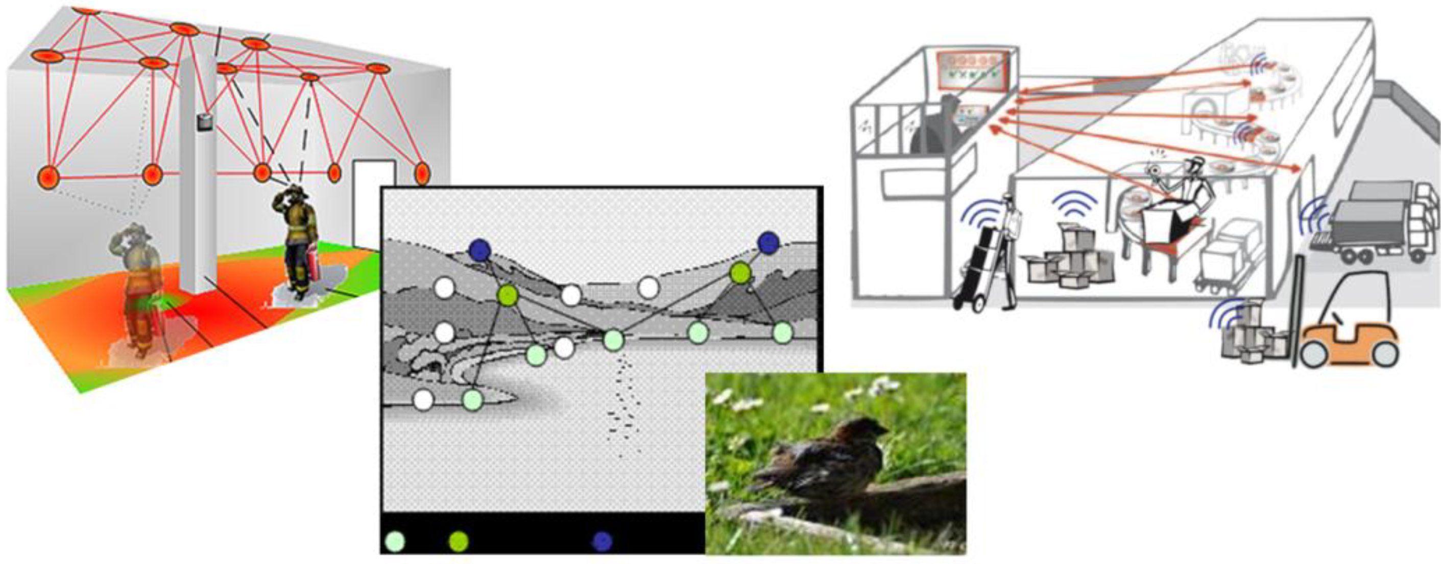
:1. Introduction

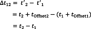
2. Localization Using Time-Difference-of-Arrival (TDOA)
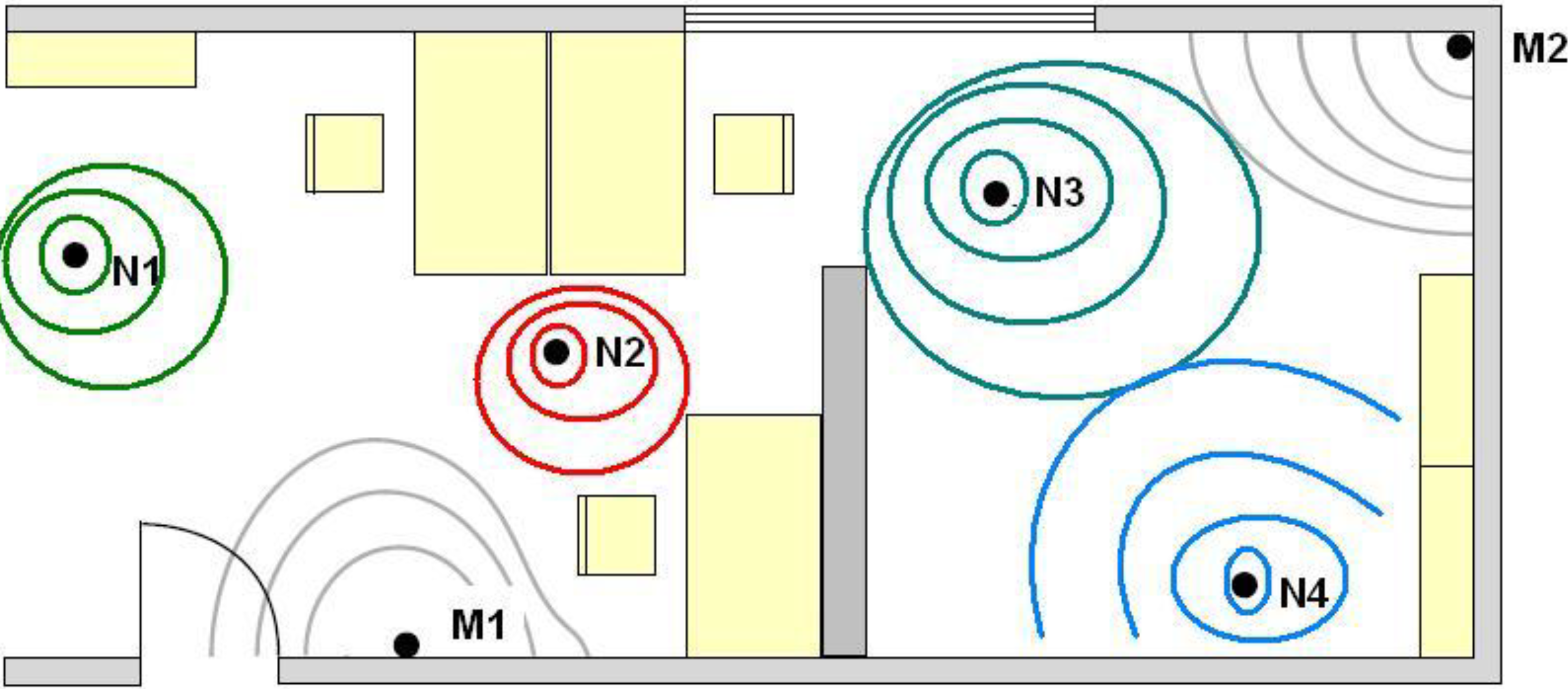

3. System Design
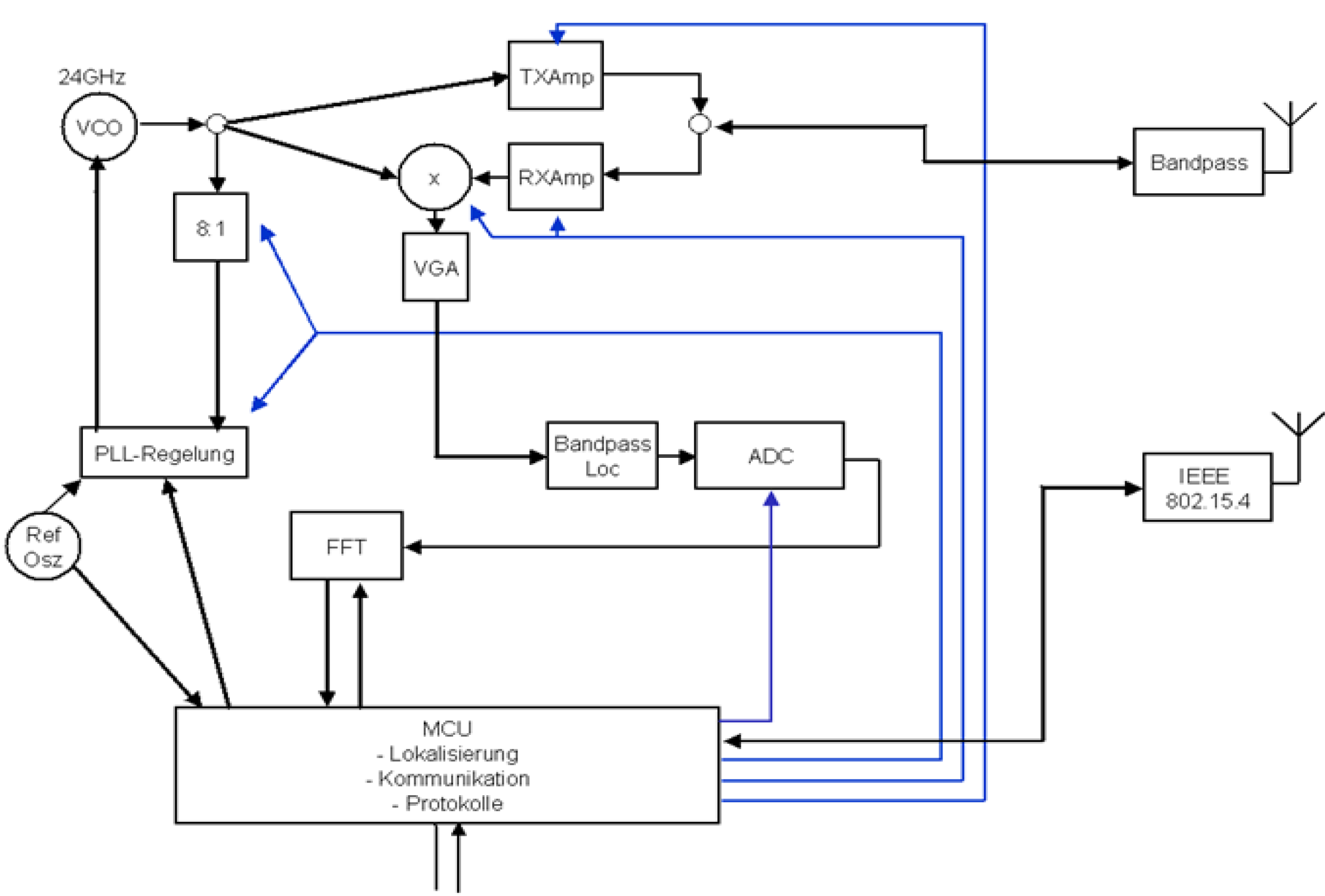
3.1. System Overview

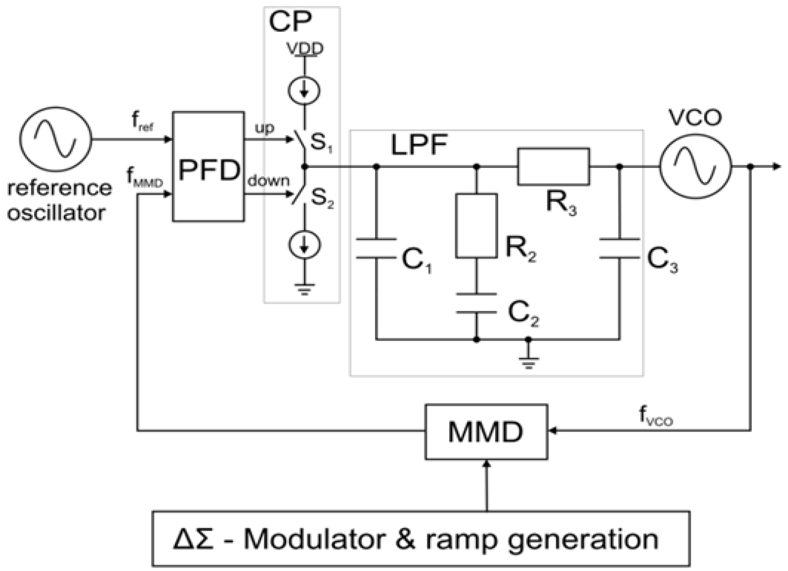
3.2. Synthesizer Concept

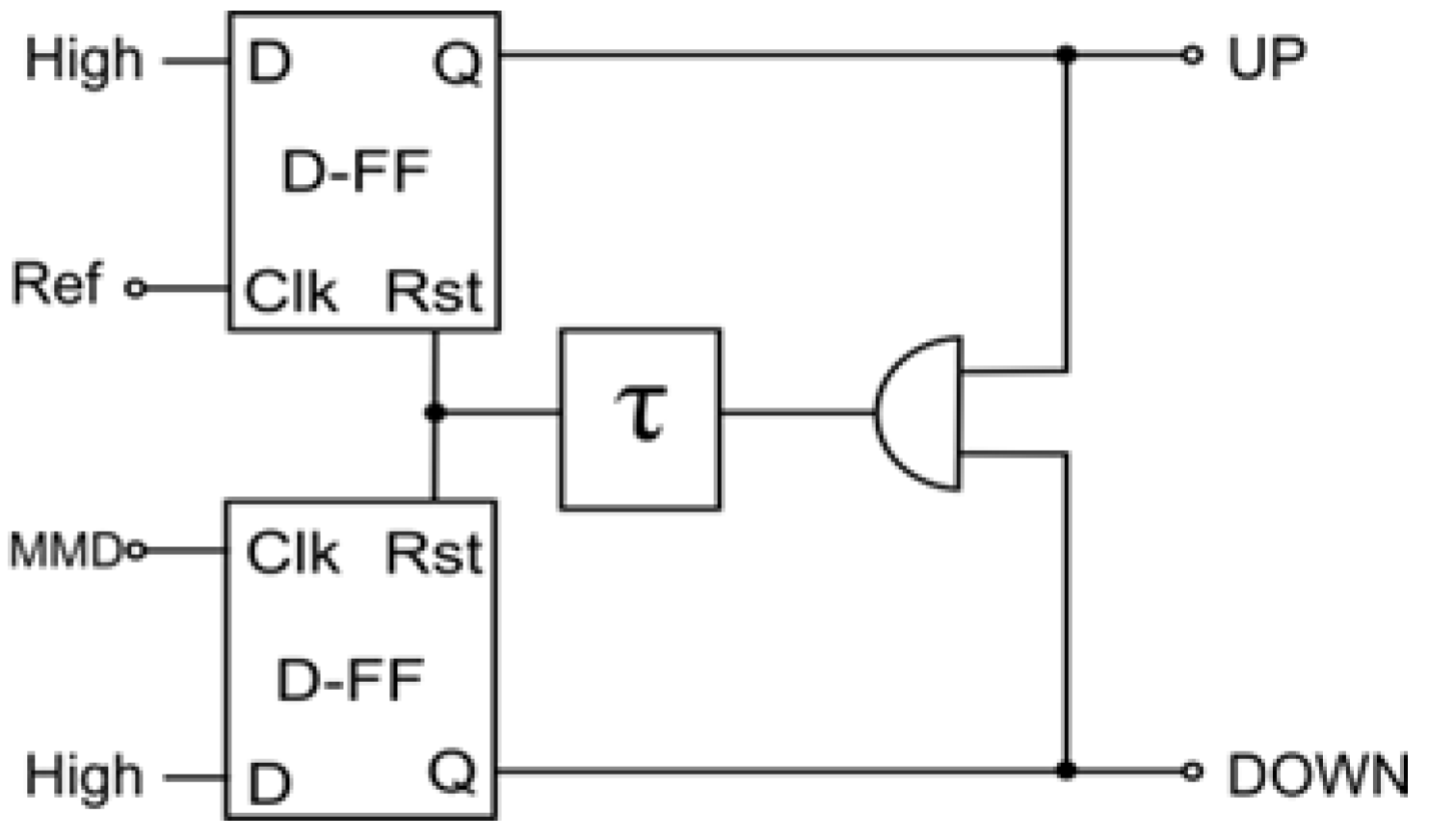
3.2.1. Phase-Frequency Detector
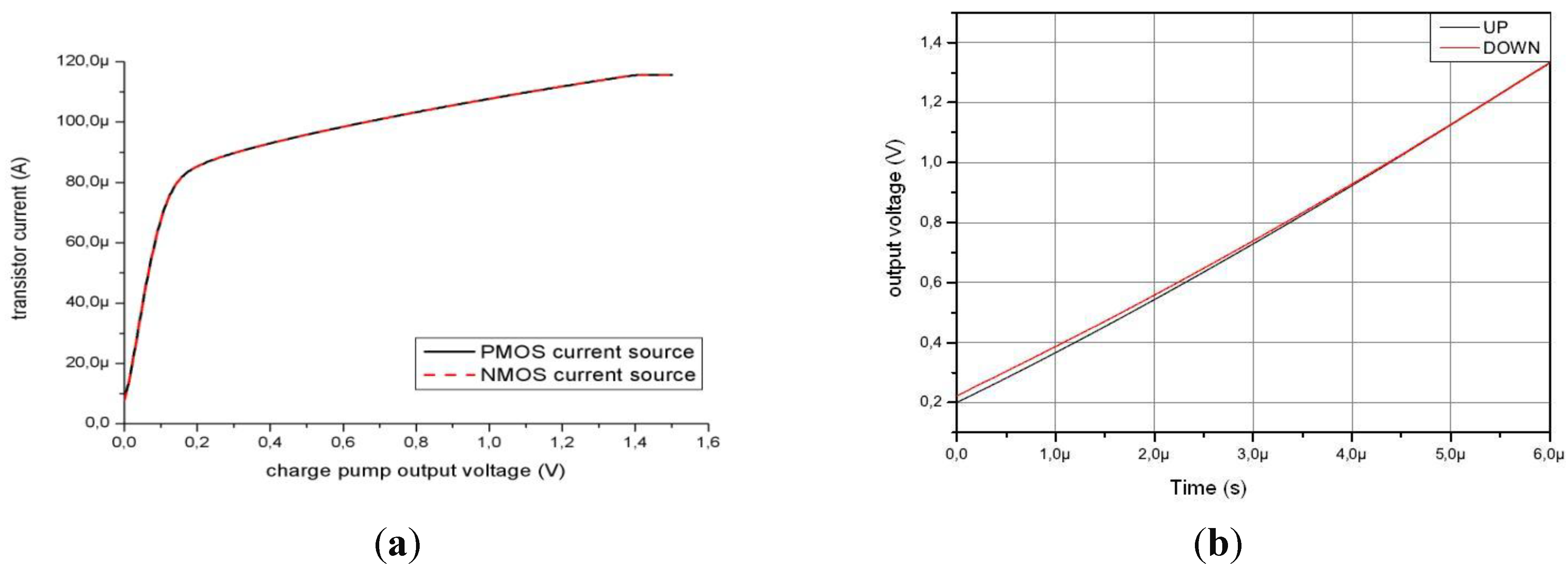
3.2.2. Charge Pump
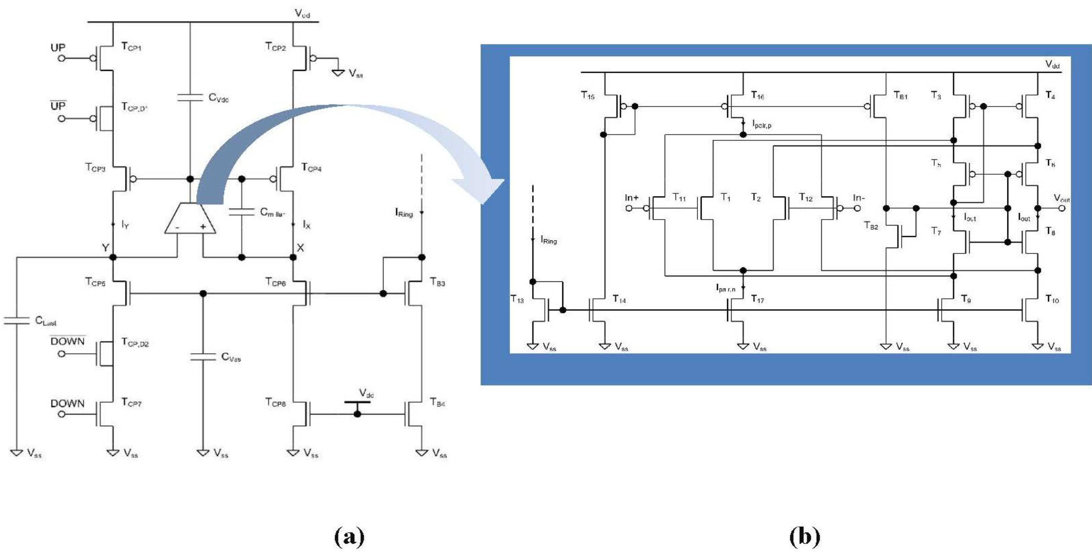
3.2.3. Improved Charge Pump Design


3.2.4. Loop Filter


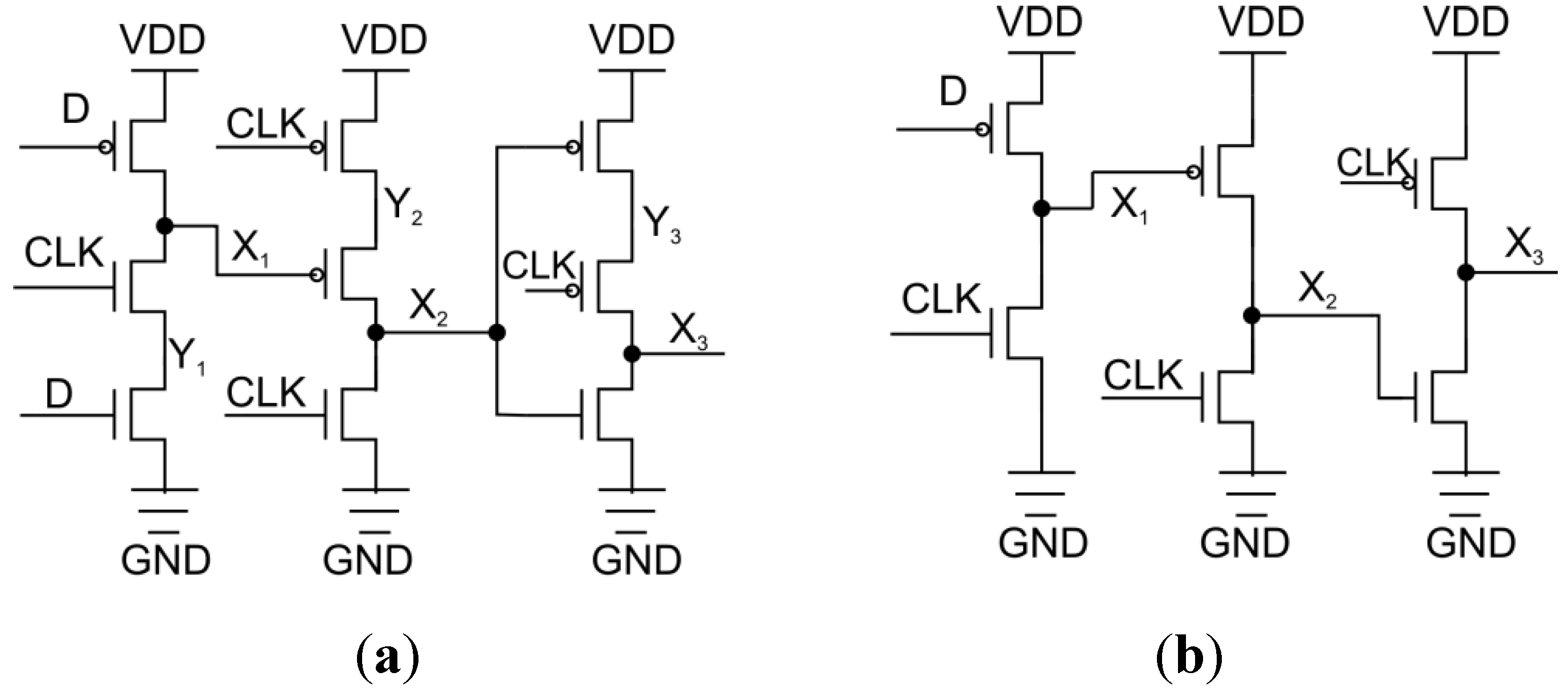
3.2.5. Frequency Divider
3.2.6. New TSPC based Static Frequency Divider

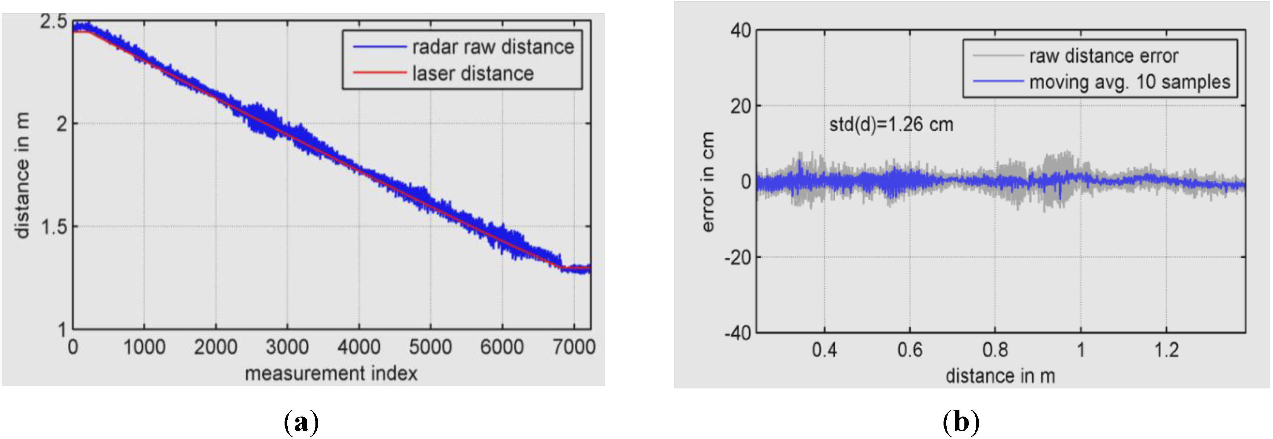
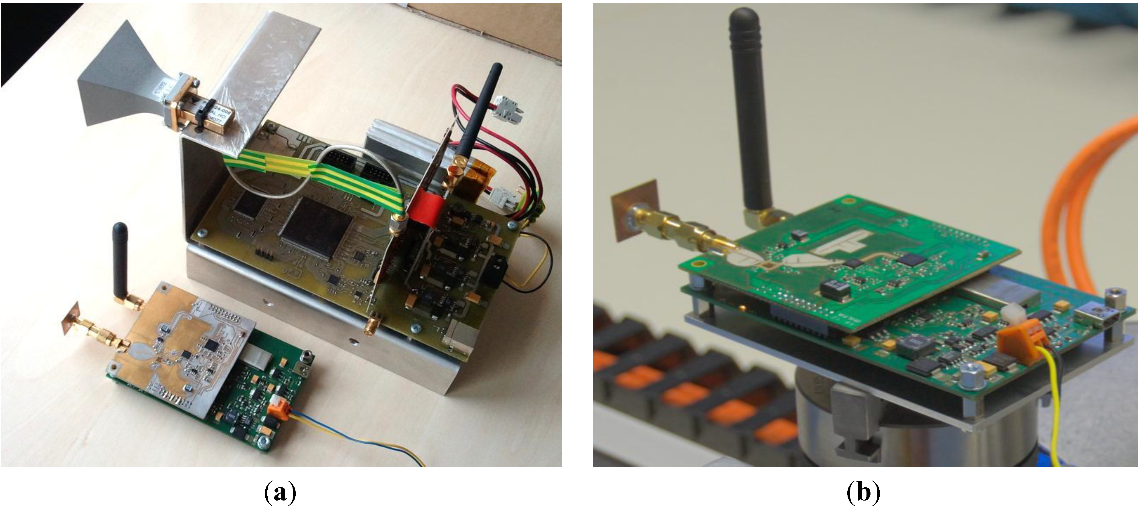
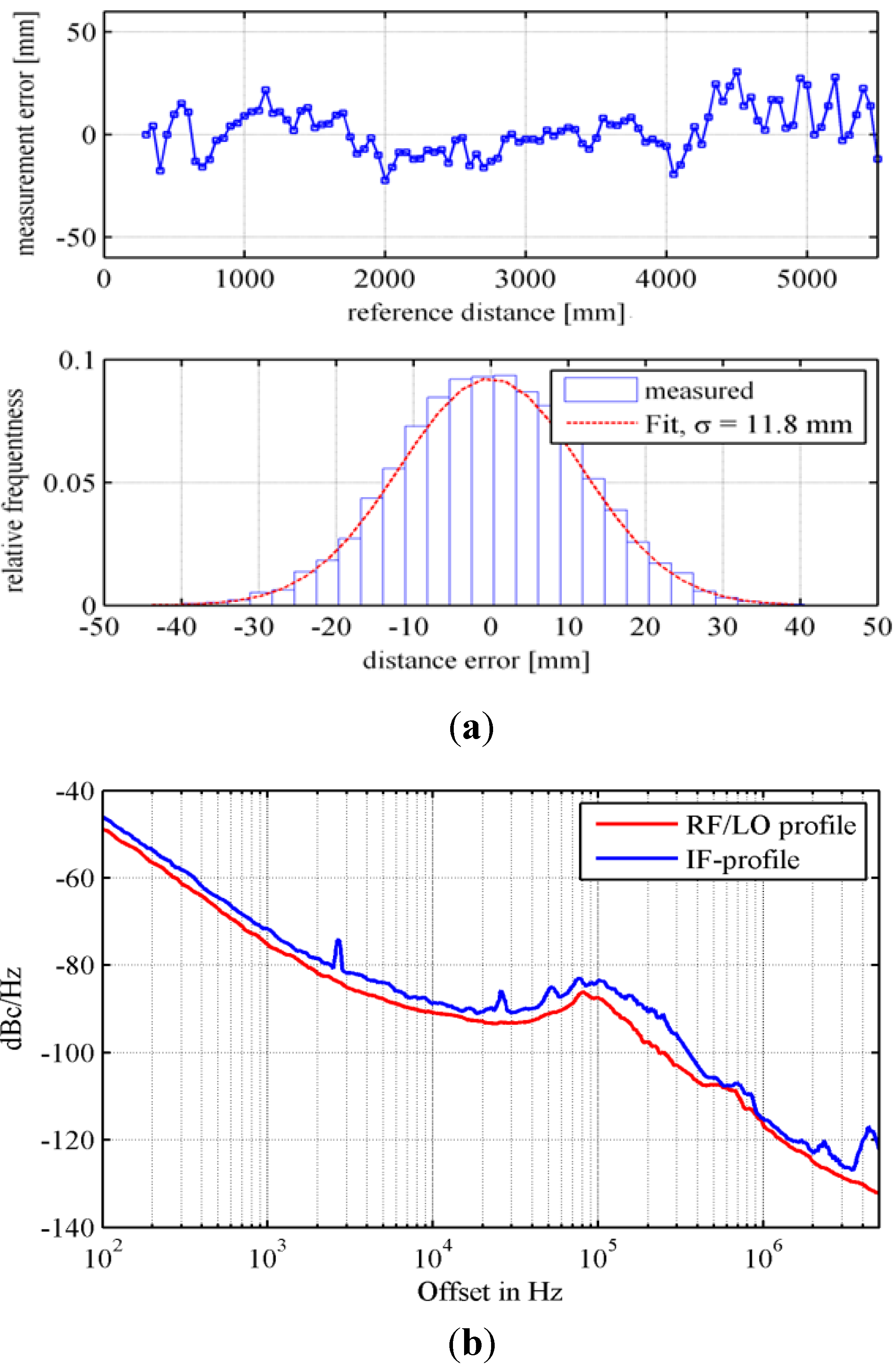
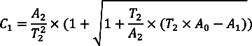
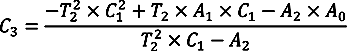
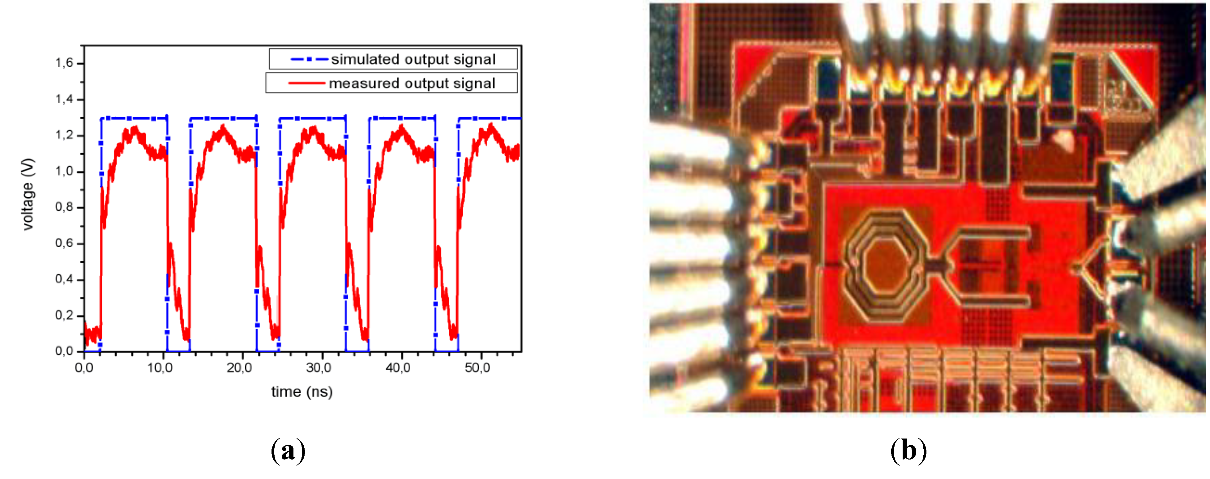
4. Prototype and Experiment


5. Conclusions
Acknowledgments
Conflicts of Interest
References
- Bundesnetzagentur. Available online: http://www.bundesnetzagentur.de (accessed on 16 July 2013).
- Roehr, S.; Gulden, P.; Vossiek, M. Method for High Precision Clock Synchronization in Wireless Systems with Application to Radio Navigation. In Proceedings of 2007 IEEE Radio and Wireless Symposium, Long Beach, CA, USA, 9–11 January 2007; pp. 551–554.
- Heidrich, J.; Brenk, D.; Essel, J. Local Positioning with Passive UHF RFID Transponders. In Proceediongs of 2009 IEEE MTT-S International Microwave Workshop on Wireless Sensing, Local Positioning, and RFID, Cavtat, Italy, 24–25 September 2009; pp. 1–4.
- Tragas, P.; Kalis, A.; Papadias, C.; Ellinger, F. RESOLUTION: Reconfigurable System for Mobile Local Communication and Positioning. In Proceedings of 2007 16th IST Mobile and Wireless Communication Summit, Budapest, Hungary, 1–5 July 2007; pp. 1–5.
- Kirsch, F.; Vossiek, M. Distributed Kalman Filter for Precise and Robust Clock Synchronization in Wireless Networks. In Proceedings of the 2009 IEEE Radio & Wireless Symposium, San Diego, CA, USA, 18–22 January 2009; pp. 482–485.
- Shmakov, D.; Ebelt, R.; Vossiek, M. Wireless Sensor Network with 24 GHz Local Positioning Transceiver. In Proceedings of 2012 IEEE MTT-S International Microwave Symposium (IMS), Montreal, Canada, 17–22 June 2012; pp. 1–3.
- Ferizi, A.; Baust, P.; Jung, M.; Fischer, G.; Weigel, R.; Koelpin, A. An Area-Efficient 130 nm CMOS Baseband Processing Unit for 24 GHz FMCW Radar Positioning. In Proceedings of 2012 International Symposium on Signals, Systems and Electronics (ISSSE), Potsdam, German, 3–5 October 2012; pp. 1–5.
- Jung, M.; Ferizi, A.; Weigel, R. A Chargepump with Enhanced Current Matching and Reduced Clock-Feedthrough in Wireless Sensor Nodes. In Proceedings of 2010 Asia-Pacific Microwave Conference, Yokohama, Japan, 7–10 December 2010; pp. 2291–2294.
- Ivanov, V.V.; Filanovsky, I.M. Operational Amplifier Speed and Accuracy Improvement: Analog Circuit Design with Structural Methodology; Springer: New York, NY, USA, 2004. [Google Scholar]
- Banerjee, D. PLL Performance, Simulation and Design, 3rd ed.; Dog Ear Pub. LLC: Indianapolis, IN, USA, 2003. [Google Scholar]
- Vaucher, C.S.; Ferencic, I.; Locher, M.; Sedvallson, S. A family of low-power truly modular programmable dividers in standard 0.35 µm technology. IEEE J. Solid State Circ. 2002. [Google Scholar] [CrossRef]
- Lacaita, A.; Levantino, S.; Samori, C. Integrated Frequency Synthesizers for Wireless Systems; Cambridge University Press: Cambridge, UK, 2007. [Google Scholar]
- Alioto, M.; Mita, R.; Palumbo, G. Design of high-speed powerefficient mos current-mode logic frequency dividers. IEEE Trans. Circ. Syst. II Expr. Br. 2006, 53, 1165–1169. [Google Scholar] [CrossRef]
- Navarro Soares, J., Jr.; Van Noije, W.A.M. A 1.6 GHz dual modulus prescaler using the extended true-single-phase-clock cmos circuit technique (E-TSPC). IEEE J. Solid State Circ. 1999, 34, 97–102. [Google Scholar] [CrossRef]
- Jung, M.; Fuhrmann, J.; Ferizi, A.; Fischer, G.; Weigel, R.; Ussmueller, T. Design of a 12 GHz Low-Power Extended True Single Phase Clock (E-TSPC) Prescaler in 0.13 µm CMOS Technology. In Proceedings of 2011 Asia-Pacific Microwave Conference (APMC), Melbourne, Australia, 5–8 December 2011; pp. 1238–1241.
- Shoji, M. Fet scaling in Domino CMOS gates. IEEE J. Solid State Circ. 1985, 20, 1067–1071. [Google Scholar] [CrossRef]
- Böck, G.; Ebelt, R.; Ferizi, A.; Fritzsch, T.; Heinrich, W.; Jung, M.; Maaß, U.; Müller, M.; Ndip, I.; Pursche, U.; et al. LOWILO—Low Power Wireless Sensor Network with Localization. In Proceedings of 2013 Öffentliches Statusmeeting Für Projekte im Bereich der, Berlin, Republic of Ireland, 18–19 February 2013; pp. 10–19.
© 2013 by the authors; licensee MDPI, Basel, Switzerland. This article is an open access article distributed under the terms and conditions of the Creative Commons Attribution license (http://creativecommons.org/licenses/by/3.0/).
Share and Cite
Jung, M.; Fischer, G.; Weigel, R.; Ussmueller, T. Low Power 24 GHz ad hoc Networking System Based on TDOA for Indoor Localization. ISPRS Int. J. Geo-Inf. 2013, 2, 1122-1135. https://doi.org/10.3390/ijgi2041122
Jung M, Fischer G, Weigel R, Ussmueller T. Low Power 24 GHz ad hoc Networking System Based on TDOA for Indoor Localization. ISPRS International Journal of Geo-Information. 2013; 2(4):1122-1135. https://doi.org/10.3390/ijgi2041122
Chicago/Turabian StyleJung, Melanie, Georg Fischer, Robert Weigel, and Thomas Ussmueller. 2013. "Low Power 24 GHz ad hoc Networking System Based on TDOA for Indoor Localization" ISPRS International Journal of Geo-Information 2, no. 4: 1122-1135. https://doi.org/10.3390/ijgi2041122