Article

Photovoltaic Energy Harvesting Wireless Sensor Node for Telemetry Applications Optimized for Low Illumination Levels

1
Faculty of Electronic Engineering, University of Niš, Aleksandra Medvedeva 14, 18000 Niš, Serbia
2
Department for Mechatronics, ITM School, Royal Institute of Technology (KTH), SE-100 44 Stockholm, Sweden
*
Author to whom correspondence should be addressed.
Electronics 2016, 5(2), 26; https://doi.org/10.3390/electronics5020026
Submission received: 24 March 2016 / Revised: 17 May 2016 / Accepted: 25 May 2016 / Published: 1 June 2016
(This article belongs to the Special Issue Energy Scavenging for Embedded Electronic Systems)

Abstract

:
This paper reports the design of a photovoltaic energy harvesting device used as a telemetry node in wireless sensor networks. The device draws power from the small solar cell, stores it into the primary energy buffer and backup supercapacitor, collects measured data from various sensors and transmits them over low power radio link at 868 MHz. Its design ensures reliable cold booting under very poor illumination conditions (down to 20 lx). The solar cell also enables indirect illumination level detection for the subcircuit that manages stored energy (day/night detector). The device is allowed to draw power from the backup supercapacitor only when it is not possible to gather enough energy from the solar cell during the sleep period. Short lasting and sudden drops of the illumination do not activate the backup power supply. A wireless sensor node design is adjusted to the proposed photovoltaic harvesting circuitry, so the overall power consumption in the sleep mode is less than 25 μW. Also, due to adaptive power consumption, proposed device topology ensures its autonomy time in the total darkness of 81 h. The device has been produced using commercially available components enabling versatile telemetric functionality by the implementation of different sensors.

Graphical Abstract

1. Introduction

Constant reduction in power consumption of microcontrollers and sensors has led to the appearance of various energy harvesting systems [1]. Those are autonomous systems powered by the energy gathered from their surroundings. The most common energy sources are ambient light, thermal gradient, airflow, vibrations or electromagnetic field [2,3,4,5,6,7,8,9,10,11,12]. Indoor environmental sources usually offer a low amount of energy (order of m W or μ W ) and proper operation of the autonomous systems is achieved by different approaches to their design. In ambients where several energy sources are available, they can be exploited simultaneously or alternatively to enable continuous power supply [13]. The indoor hybrid energy harvesting devices usually exploit ambient light in conjunction with thermal energy sources [6,9], vibrations [9,10], airflow [12] or electromagnetic induction [9]. These devices either have only one power management circuit in order to reduce complexity and dissipation [6,14], or an optimized power management circuit for each energy source to obtain increased efficiency of the whole system [9,12]. Considering only ambient light, indoor conditions can provide up to several hundreds of μ W · cm - 2 , mostly from the artificial sources, which demands ultra low–power energy harvesting. It is to be noted that the term “indoor” may also refer to the outdoor environment characterized by the low illumination levels.
Energy harvesting systems are widely used as telemetric nodes in wireless sensor networks (WSNs) [15]. In most cases, nodes of the network are designed to collect data from different sensors and transmit them to the control unit in predefined time intervals. Thus, operating cycle of the node consists of the two operating modes – active and inactive (sleep). During the active mode, node performs data acquisition and transmission. Usually, these operations last very short, around a few tens of milliseconds. WSN node spends much more time in the inactive mode in order to preserve energy and this period lasts from few seconds to few minutes. Ratio of the active and inactive periods represents operating duty cycle of the node, which may be pretty low and ranges approximately from 0.005% to 5%. When the node is inactive, WSN does not “care” if it is in the sleep mode or has lost power supply. The WSN nodes aimed for ultra low–power applications operate non–perpetually with low duty cycle, have optimized number of sensors for data acquisition, and perform data transmission radio frequency (RF) activity.
The main technical issues of the low–power photovoltaic energy harvesting concern the amount of collected and transferred energy, storage elements, and cold booting [16]. Increase of the amount of collected ambient light (especially under low illumination levels) can be achieved by usage of the flat panel reflectors in conjunction with the photovoltaic (PV) cell [17].
The amount of energy transferred from the harvesting device to the load is controlled by the appropriate interface circuitry which usually contains one or more energy storage elements. Some interface circuits are based on the boost converter architecture [18,19,20], while in the other, maximum power point tracking (MPPT) technique is used. Under low illumination levels the amount of harvested energy over time may be comparable to the power consumption of commercial MPPT integrated circuits [21], and therefore, special approaches to this technique are proposed. An ultra-low power MPPT method for illuminations above 200 lx is presented in [4]. A sample–and–hold based MPPT technique for illuminations above 100 lx is described in [22]. In [23], an analog MPPT circuit is implemented by using fractional open circuit voltage algorithm for illumination of 200 lx .
Over the last few years, there have been reports on the on-chip photovoltaic energy conversion/ management circuits. They are manufactured in the nm scale CMOS technology, enabling nA or μA sleep current with [24,25] or without [26,27] implemented MPPT technique. There are also commercial ICs dedicated to indoor light harvesting which operate with low input/start–up voltage, implement MPPT technique and have low quiescent current [28]. However, these ICs can not perform telemetric and large storage charging activities simultaneously.
Two different ways for storage of the harvested energy are most common among various devices. One employs a large storage element to power the system. That is usually a supercapacitor [29,30,31], a battery [27], or a combination of both [3,32]. Selection of the battery or supercapacitor is usually based on their energy or power density, number of charge–recharge cycles, leakage current and complexity of the charging circuit [4]. Since the large storage element requires a long time to be charged to the usable voltage level, it has a slow cold booting (zero–energy system start–up). Larger PV cells provide higher charging currents but that implies oversized harvesting system. In that sense, the second way of energy storage implements an additional element known as a “primary energy buffer” (also designated as a bootstrap capacitor). It has smaller capacity than accompanied larger storage element, known as a “backup storage” or a reservoir capacitor. The role of the primary energy buffer is to enable quick system start–up [33]. In some applications, it needs to be pre–charged to obtain power until the backup storage is charged enough to take over [3].
Reliable cold booting of the system demands its start–up without any disturbances of the operation. A high start voltage value is most common way to solve this issue [16], despite degraded efficiency of such a system. Another way is usage of a Schmitt trigger to postpone the system start until energy storage is sufficiently charged. However, the powering of the Schmitt trigger itself and its reliable switching off remain as problems [16]. The integrated start–up circuit presented in [34] produces a power–on–reset signal for the energy harvesting system and temporarily shunt the output of the PV cell voltage till step–up converter starts operating. The cold–start block from [22] incorporates a capacitor which provides a power supply to the astable multivibrator and sample–and–hold blocks for illuminations above 100 lx . A software solution proposed in [35] enables different operating modes of the microcontroller depending on the charge level of the storage.
The choice of storage elements and their power management circuit is also related to the WSN node autonomy. The primary goal is to achieve at least 12 h autonomy in total darkness with fully charged backup storage element. Appropriate power management circuit can obtain extended node autonomy due to the lower discharging current [36], or by forcing use of the ambient energy as long as it is possible [37]. Another approach is to optimize the storage capacity to satisfy the energy neutral operation condition [31]. The overall WSN efficiency can be alternatively increased by an energy–aware sensor node design. It is accomplished on the node or/and network level, and most often is based on different data processing algorithms [38], or calculation of the lowest power needed to transmit the measurement data [39].
The system presented in this paper is designed to partially overcome issues related to the low illumination energy harvesting and enable reliable telemetry operation and extended autonomy. The device is comprised of the photovoltaic energy power supply and the WSN node which measures temperature and air humidity and transmits data. Device architecture, presented in Section 2, enables reliable cold booting and extended autonomy in the total dark conditions. The harvesting part incorporates primary and backup energy storages which are dimensioned in Section 3. It includes a novel day/night (extremely low illumination level) detector subcircuitry. Detector forces power supply from the primary storage as long as the illumination level is high enough to allow at least one operating cycle of the WSN node. It does not require a separate sensing element for the illumination level. Instead, a single solar cell is used as a charger and an indirect illumination level sensor. In order to exclude all circuit elements which can extensively consume power during the sleep mode, device neither performs MPPT nor contains buck/bust converter. It is practically realized in a form of a prototype and its performance evaluation results are presented in Section 4.

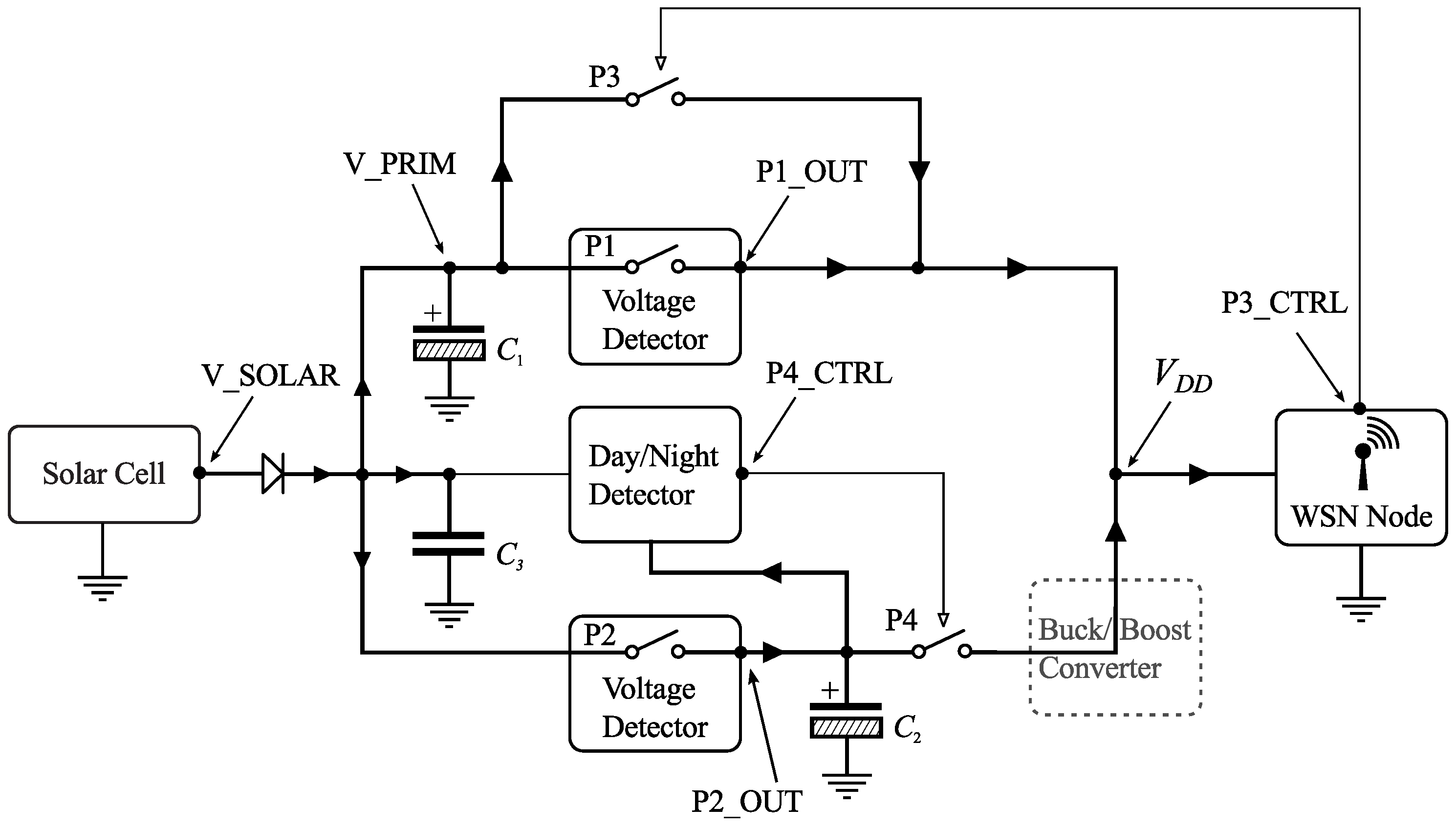
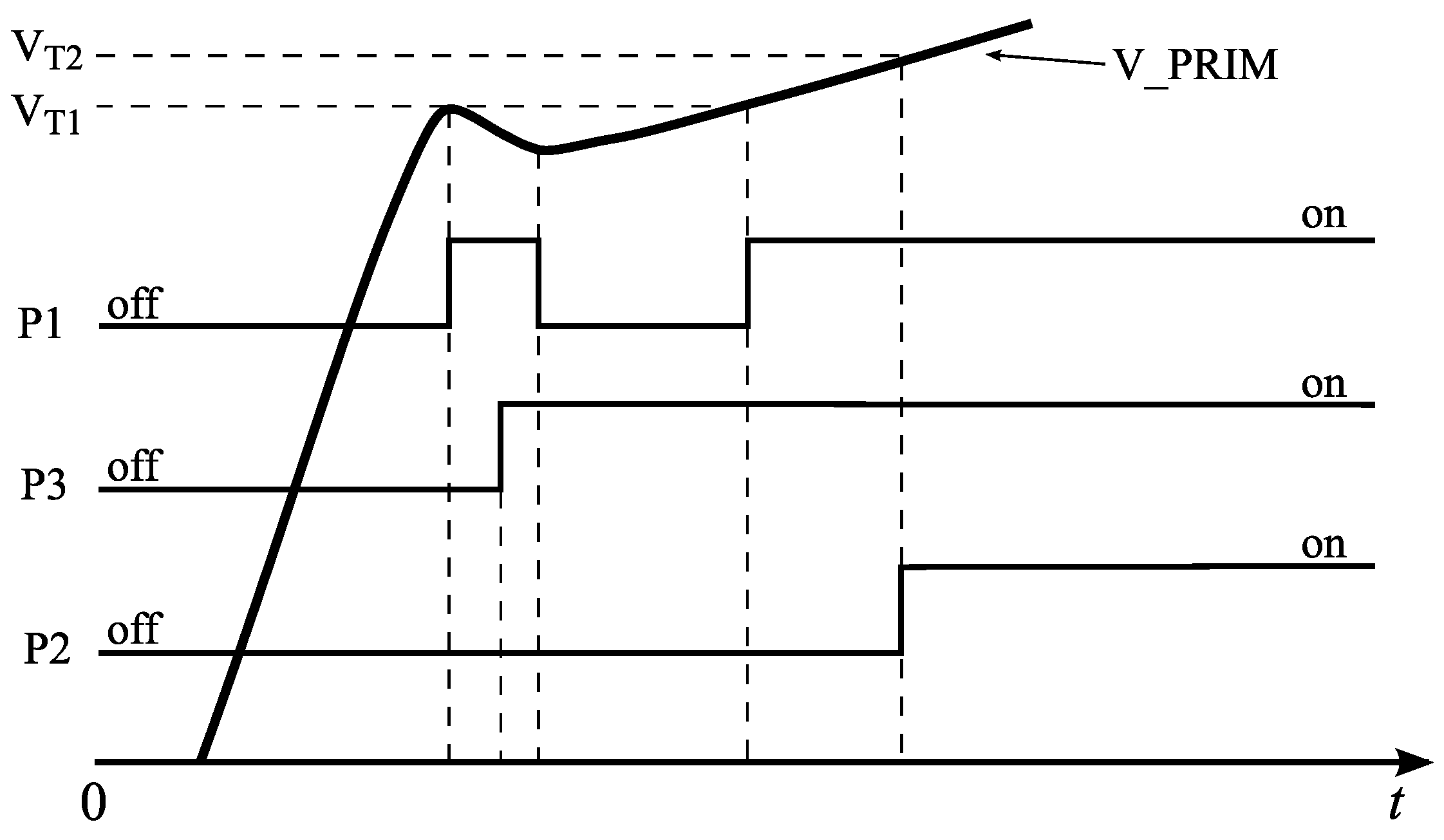
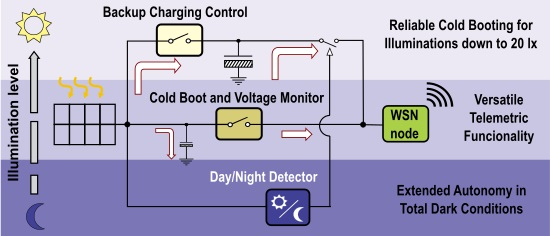
2. Device Architecture

Block diagram of the proposed system is shown in Figure 1.
Capacitor C 1 represents primary energy buffer, while C 2 is backup supercapacitor. The role of switches P1–P4 is to control the route of the harvested energy. Switches P1 and P2 contain high precision voltage detectors that have very low power consumption proportional to their input voltage level [40]. Their threshold voltages are V T 1 = 2 . 1 V and V T 2 = 2 . 4 V , respectively. The value of V T 1 is set to be higher then WSN node minimal operating voltage V D D m i n = 1 . 8 V to avoid multiple faulty boot attempts. Once the cell is illuminated, switch P1 is turned on when the voltage V _ PRIM reaches V T 1 , as illustrated in Figure 2.
The WSN node receives power supply V D D and starts to boot. During the booting process, the node has excessive power consumption and the voltage V _ PRIM decreases abruptly. This turns off P1, which would eventually cut off the power to the node. However, the switch P3 is controlled by the node, and it is being switched on immediately upon the power up of the microcontroller. The switch P1 is effectively bypassed and the node receives continuous supply directly from C 1 . Therefore, the switch P3 ensures reliable cold booting, even at low illumination levels and helps to avoid oversized device due to the high value of V T 1 or large solar cell. It is released when the condition V _ PRIM V D D m i n is met, and the node can not be supplied from the primary section. Although the Schmitt trigger can eliminate P1, it has limitations described in Section 1.
If the amount of harvested energy over time is higher than power consumption of the WSN node, excess energy is stored in C 2 . It starts charging when the voltage V _ PRIM reaches V T 2 and the switch P2 turns on, as presented in Figure 2. Overvoltage protection of the device was realized using two LEDs with low leakage currents connected in series and set parallel to the solar cell.
In indoor applications, it is highly possible that power consumption of the WSN node exceeds the amount of energy harvested from the PV cell. In this case, one approach is that WSN node starts to draw power from the backup storage immediately. If the backup storage is charged enough, the node preserves functionality, but if it is empty, the node is left without power [3]. The proposed system introduces different usage of the energy stored in the backup. The day/night detector decides if the node should be powered from the primary or backup section. It obtains information indirectly, by monitoring the solar cell voltage. This simplifies the system because it does not require additional sensors like the pilot cell or light dependent resistor [3,5].
Schematic of the harvesting block, including semiconductor devices that protect storage elements from unnecessary discharging, is presented in Figure 3.
Note that switch P3 is the circuit comprised of transistors Q 1 and Q 3 , while P4 is essentially transistor Q 6 [41,42].
Capacitance C 3 is very small in comparison to C 1 , and both are charged simultaneously. By monitoring voltage on C 3 , it is possible to know the solar cell voltage, as well as the primary energy buffer voltage. Detector should prevent usage of the energy stored in the backup as long as the voltage V _ PRIM is above V T 1 . It contains low power comparator [43] which is powered from the backup supercapacitor. Because the comparator has a fixed internal voltage reference of 1.245 V, its input voltage is adjusted to be proportional to the voltage V _ PRIM by using a resistive divider. When V _ PRIM drops below V T 1 , after the delay τ = C 3 ( R 9 + R 10 ) , the comparator turns on the switch P4 and the WSN node starts to be supplied from the backup supercapacitor. By introducing the delay, false triggers of the comparator, which may occur due to the sudden short illumination changes and subsequent solar cell voltage drops, are prevented (because C 3 discharges slower than the illumination change lasts). Also, eventual recharging of C 1 above V T 1 during the delay preserves the backup charge. This recharging time is relatively short because the node does not deplete primary storage down to zero, so the cold booting is avoided. Thus, the node has extended autonomy at poor illumination levels. Only when the illumination level is low for prolonged period of time, the day/night detector enables WSN node to use energy from the backup through P4. The voltage detector U 3 [40] is used to prevent unnecessary discharging of C 2 if it is being charged to a voltage less than V T 1 .
During the design of the harvesting block, two methods of the backup energy usage were considered. The first method implements buck/boost converter block, located between the switch P4 and WSN node (Figure 1). The converter is considered in order to provide constant supply voltage to the WSN node during the night. Another method is to power the WSN node directly from the backup energy storage, and it is adopted because of the advantages discussed in Section 4.
Besides the efficiency of energy harvesting circuitry, it is also very important that the WSN node consumes as little power as possible. Because the node with low duty cycle spends most of the lifetime in sleep mode, it is essential to minimize its power consumption during this period. Block diagram of the realized WSN node is shown in Figure 4.
The node consists of a microcontroller, a radio module, and a temperature/humidity sensor. Particular devices are chosen primarily because of their low power consumption in the sleep mode. The PIC18F25K20 microcontroller [44] with enabled watchdog timer and the MRF89XAM8A radio module [45] operating at 868 M Hz are implemented. The Si7005 sensor [46] has dual sensing element in one package and thus increases the system versatility.

3. Storage Elements

The capacitances of the primary energy buffer and the backup storage are sized according to the relations between their discharging currents and voltage changes during the time periods of interest. Capacitor voltage V c ( t ) decreases over time from its starting value V c ( 0 ) due to discharging with the constant current I d i s as:
V c ( t ) = V c ( 0 ) - I d i s C · t .
Accordingly, capacitance sufficient to retain voltage level above the preset value V c ( t d i s ) , while discharging during the time period t d i s is:
C = I d i s · t d i s V c ( 0 ) - V c ( t d i s ) .
The system current consumption may be averaged over time as:
I a v g = i = 1 n I i t i i = 1 n t i ,
where every product in the sum represents a portion of the total charge depleted from the storage element during each of n distinctive periods of the operation.
The primary energy buffer C 1 , when charged to V T 1 , has to supply the WSN node with enough energy during the start–up period t s , consisting of the microcontroller power–up time t m , and periods required for the radio module configuration t r f c , data acquisition t a c q and RF transmission t r f t . The average current during the start–up period is obtained on the basis of Equation (3) as:
I s = I m t m + I r f c t r f c + I a c q t a c q + I r f t t r f t t m + t r f c + t a c q + t r f t .
All quantities on the right–hand side of Equation (4) are known, either from the datasheets or from the direct measurements on the particular devices (where applicable), as shown in Table 1.
For the worst case design purposes, it is assumed that C 1 discharges with constant current I s during start–up period t s to the value V D D m i n , so it can be sized as:
C 1 = I s · t s V T 1 - V D D m i n .
From Equation (5) the value of C 1 = 905 μ F is calculated. By taking into account tolerances for the standard capacitors, the value of 2 × 470 μ F is adopted as the minimal one.
When the WSN node is powered only from the backup section, its autonomy depends on the average current consumption during one operating cycle:
I o p c = I a c q t a c q + I r f t t r f t + I s l t s l t a c q + t r f t + t s l ,
where t s l and I s l represent sleep period and the corresponding current consumption, respectively. By using Equation (6) and data from Table 1 the value of I o p c = 7 . 7 μ A is calculated.
A supercapacitor is chosen as the backup storage, primarily due to its long life cycle [30]. For a desired period of autonomy t a u t , its capacitance can be calculated as:
C 2 = I o p c · t a u t V B m a x - V B m i n ,
where V B m a x and V B m i n are the maximum and minimum voltages on the supercapacitor, respectively. The maximum backup voltage is limited to V B m a x = 3 . 77 V , in order to protect the WSN node from the overvoltage. The value V B m i n = V T 1 - 0 . 1 V = 2 . 0 V is the turn off voltage of the voltage detector inside the day/night detector (Figure 3). Note that 0.1 V is subtracted due to the voltage detector built–in hysteresis [40].
The primary goal when designing backup section was to achieve at least 12 h autonomy in total darkness with the fully charged supercapacitor, i.e., to have enough energy to operate during the night. Using Equation (7) and standard supercapacitor values, this leads to C 2 = 220 m F . However, in order to explore autonomy with and without buck/boost converter, a value C 2 = 1 . 5 F is adopted ([47], NF series), giving t a u t 96 h . Considering that the capacitance tolerance of the supercapacitor may range from –20% to 80%, this is a rough approximation.

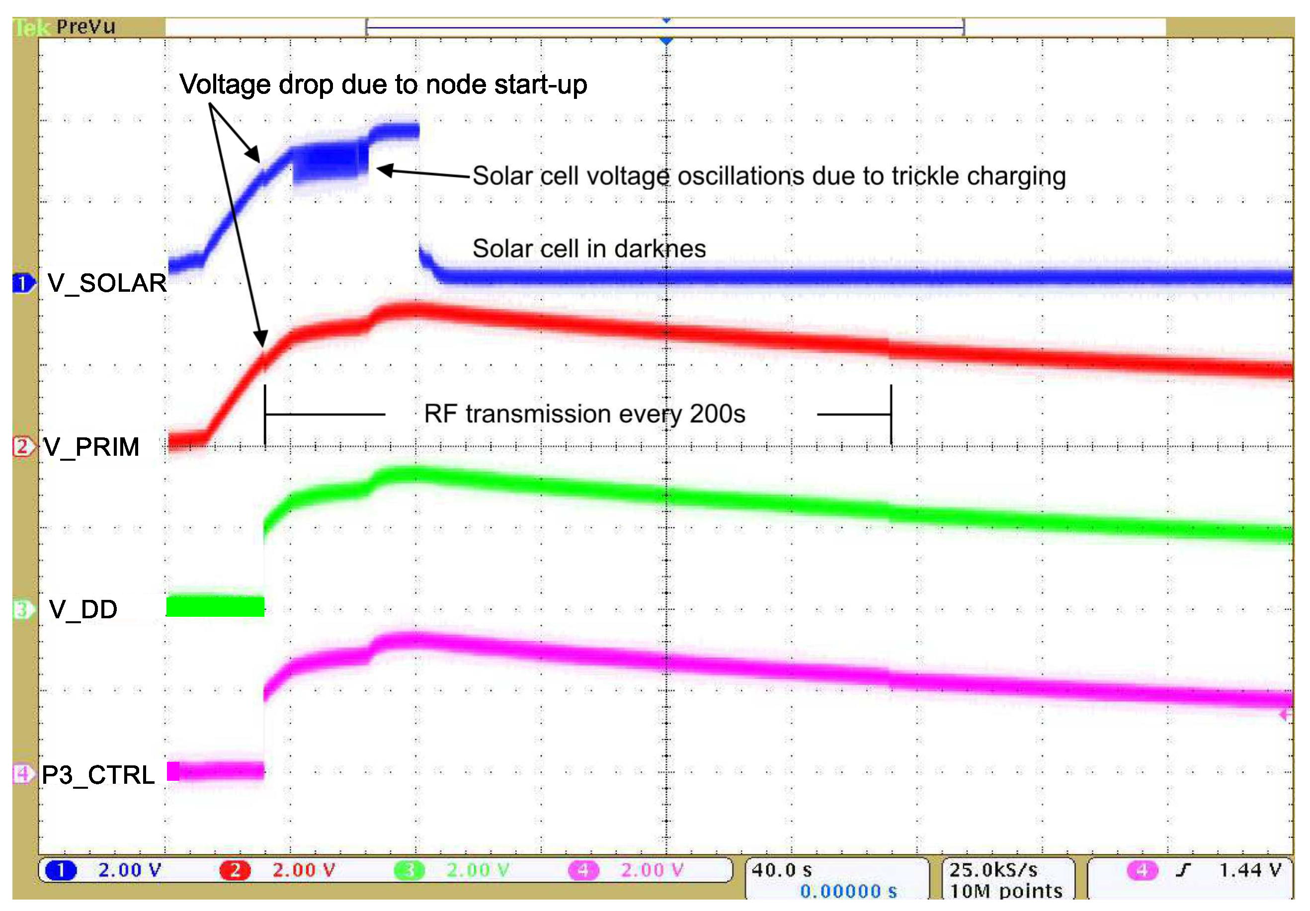
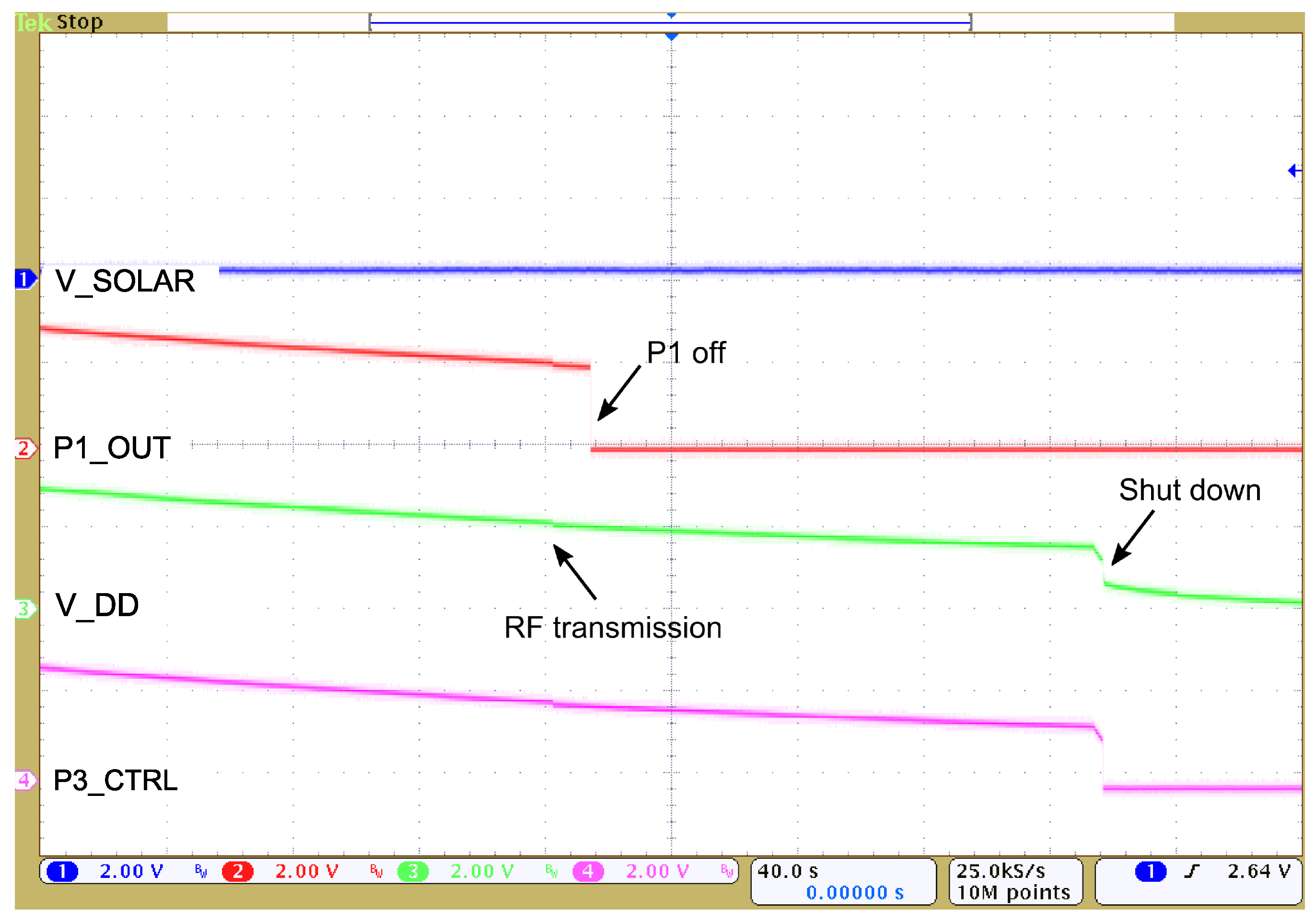
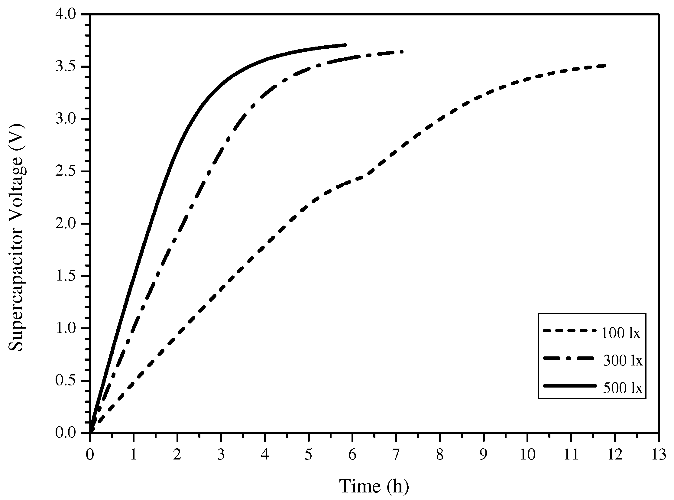
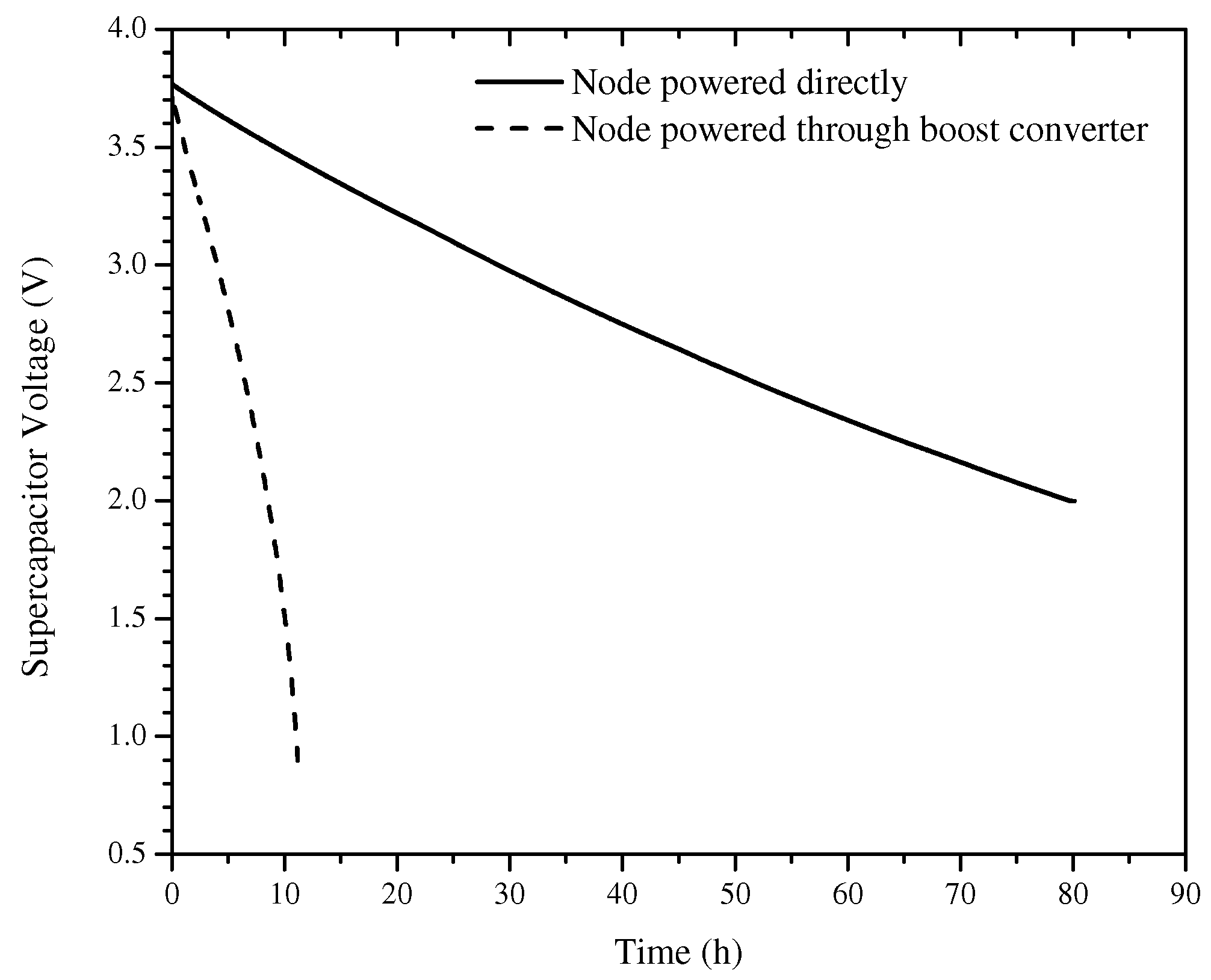
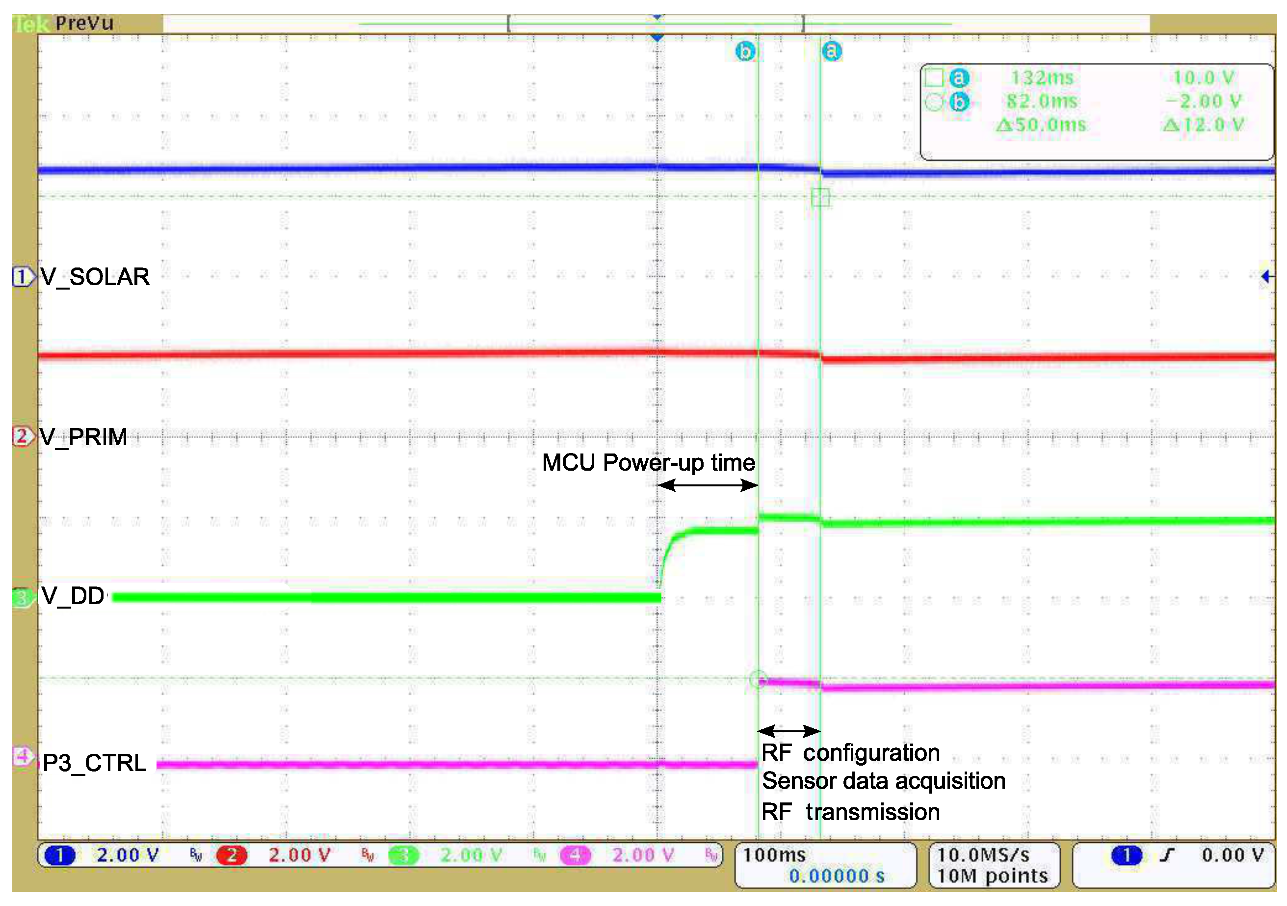
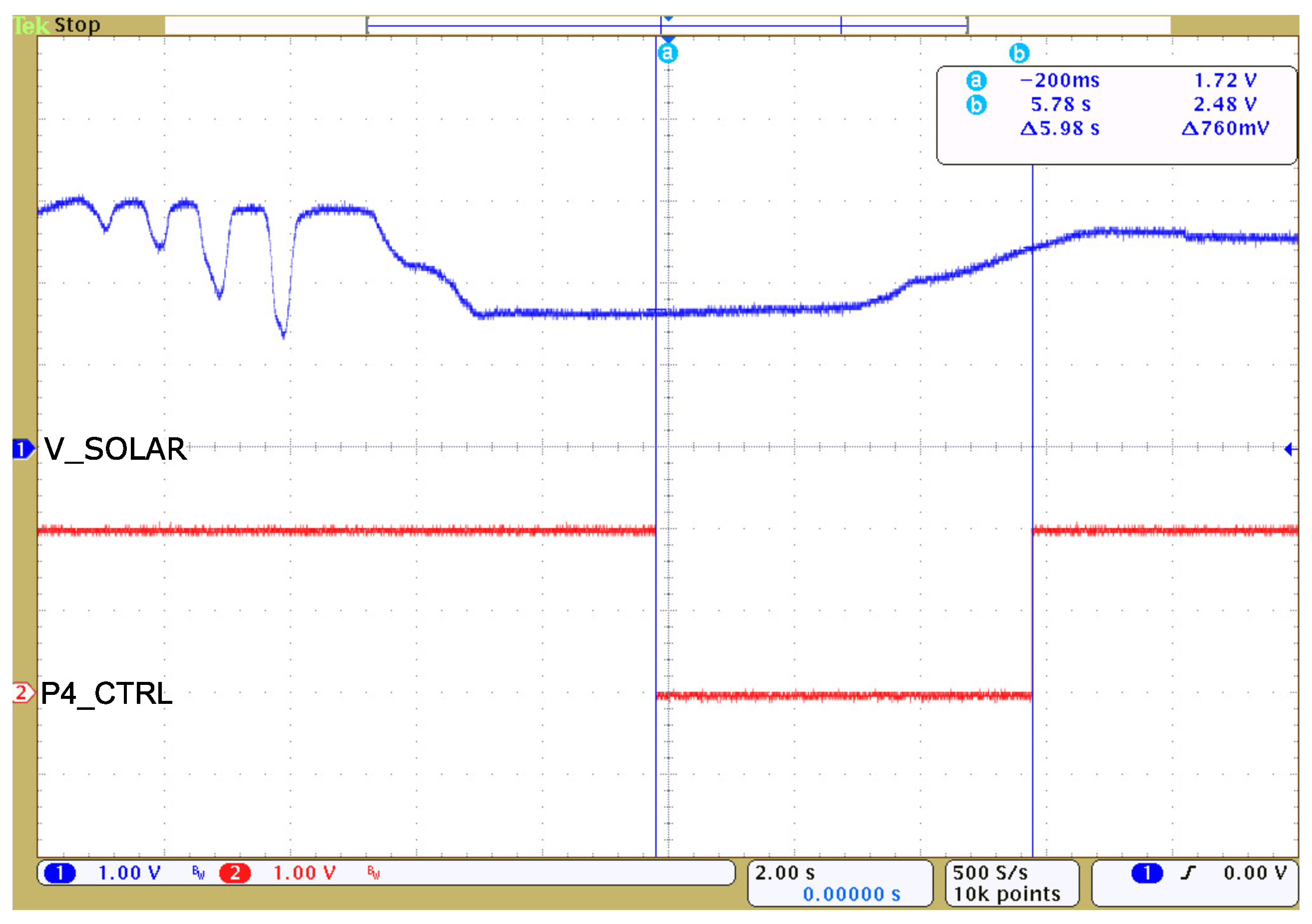
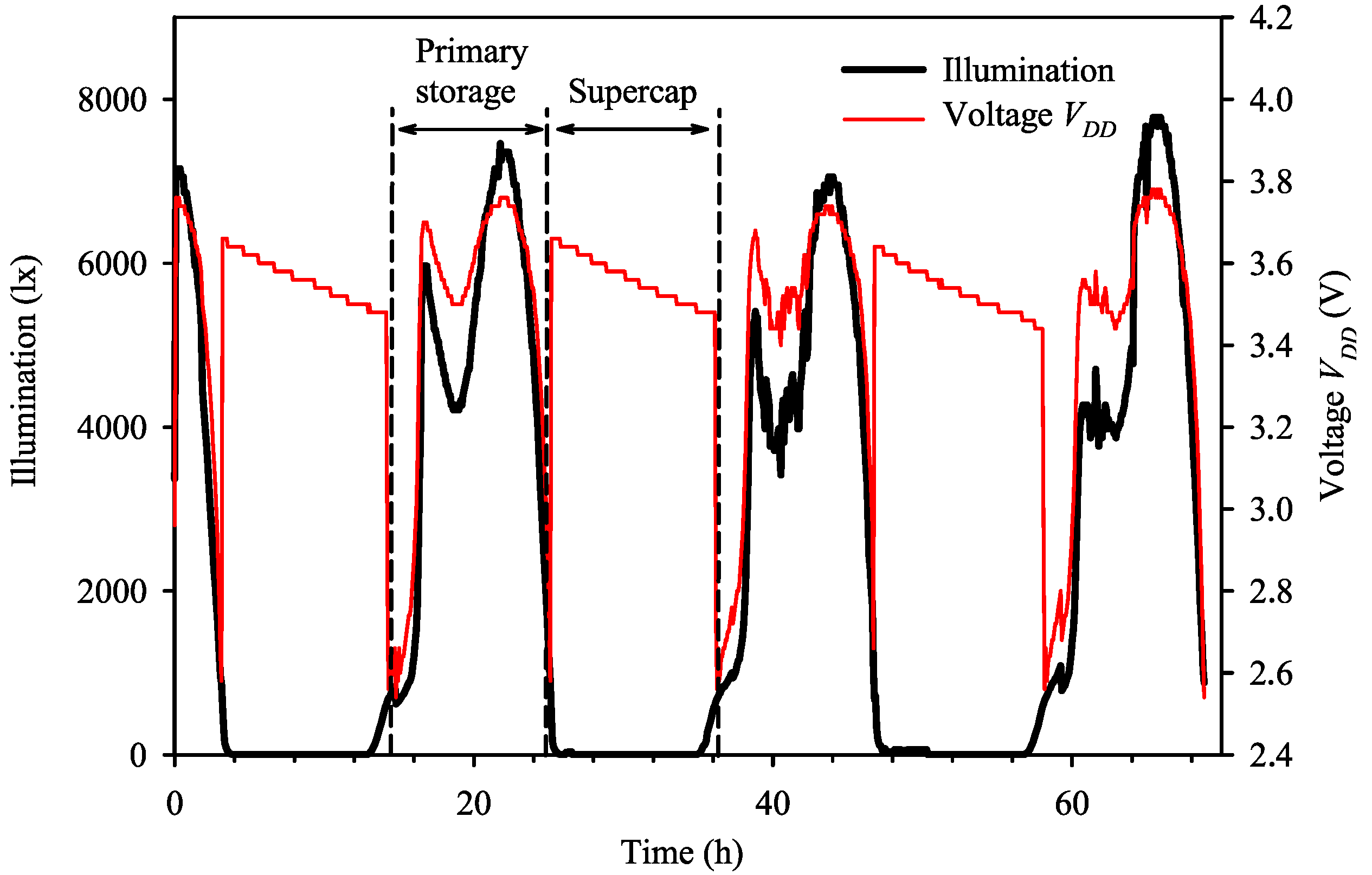
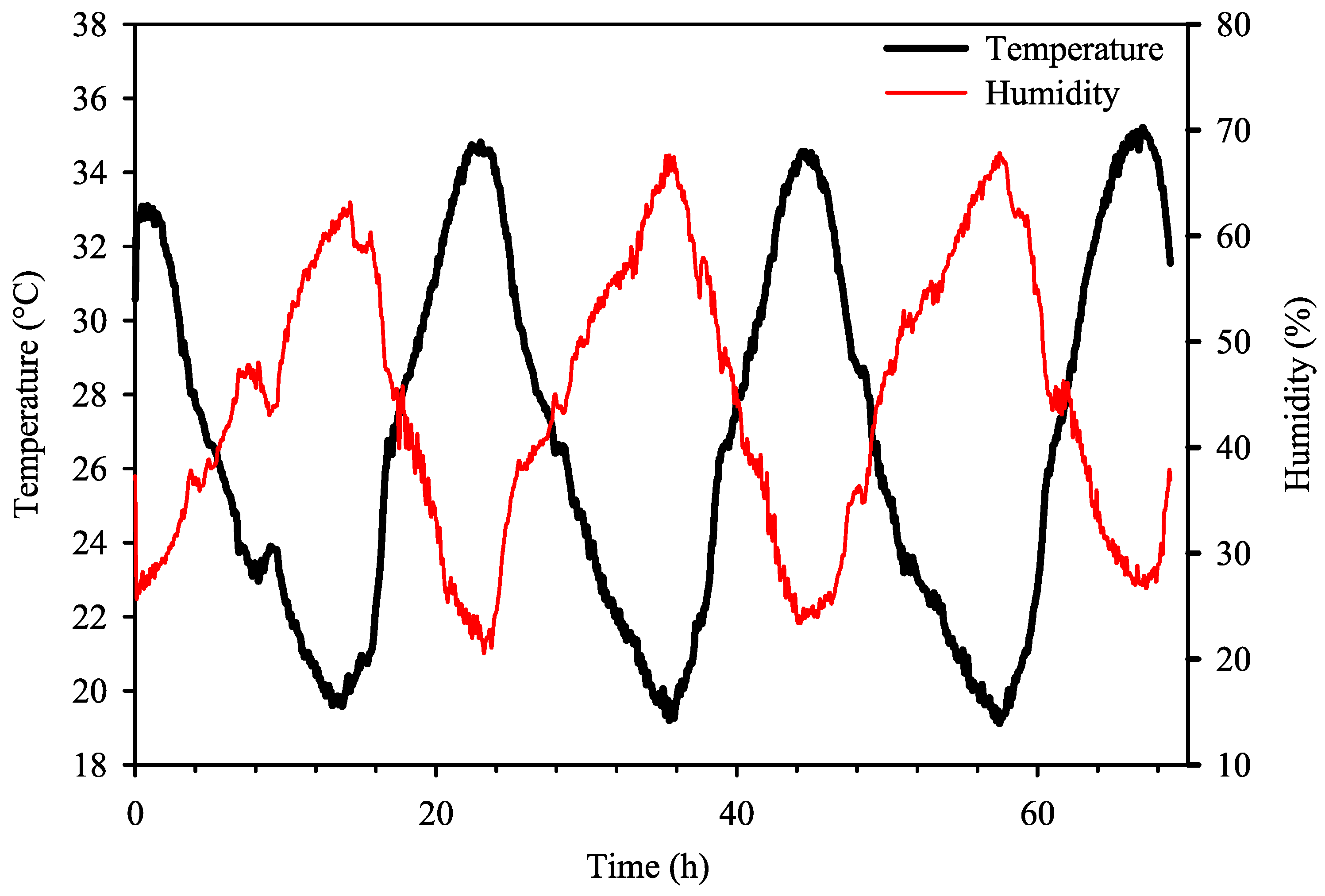
4. Experimental Results

The complete device is practically realized in a form of a prototype, using conventional printed circuit board (PCB) technology, as shown in Figure 5. A monocristaline, high efficiency solar cell SLMD600H10 [48], having area of 35 × 22 mm 2 , is used. During the measurement, WSN node was acquiring temperature and humidity data from a sensor and transmitting a packet consisting of 12 bytes (preamble–1, sync word–4, address–1, sensor readings–4, CRC checksum–2) every 200 s . At low illumination levels, the device was characterized by using an incandescent light bulb with the nominal power of 21 W as a light source. The power dissipated on the bulb was controlled by the power supply Agilent E3646A (Keysight, Santa Clara, CA, USA), while the illumination level was measured with datalogging light meter Extech HD450 (Extech, Nashua, NH, USA). Current and voltage values in the circuitry were logged by using digital multimeter Keysight 34461A (Keysight, Santa Rosa, CA, USA).
Current consumption of components during distinctive periods of the system operation are listed in Table 1. The harvesting circuitry consumes typically 3.7 μ A at 3 V supply, while the microcontroller in the sleep mode draws less than 1.2 μ A . The choice of wake–up mechanism for the microcontroller is a matter of trade–off. Among many techniques, dedicated watchdog timer is chosen for this device, and its counting cycle is predefined in firmware to 200 s . Radio module in power saving operation mode requires around 100 n A , and this is voltage independent. The sensor is active only during data acquisition and communication with the microcontroller (about 40 m s ) and its power consumption is not considered to be of primary importance. Constant, voltage independent, leakage current of the supercapacitor is around 0.5 μ A . Therefore, the whole device in the sleep mode consumes approximately 6.6 μ A . The consumption is reduced as the power supply voltage (primary/backup storage voltage) decreases.
The cold booting process and one operating cycle at high illumination level are illustrated in Figure 6.
When the WSN node receives power, the microcontroller goes through the power–up procedure which is followed by the RF module configuration, data acquisition and transmission.
A closer view of the start–up period is shown in Figure 7.
A small voltage drop is observed when the first RF transmission occurs and after that WSN node goes to the sleep mode. Due to the high illumination level, despite WSN node power consumption, the primary energy buffer is being charged from the solar cell and the voltage across it continues to rise.
When V _ PRIM reaches the threshold voltage V T 2 , the process of charging the supercapacitor starts. At the beginning of this process, oscillations of the solar cell voltage V _ SOLAR are observed (Figure 6). Maximum supercapacitor charging current of a few m A may be provided by the solar cell only at very high illumination levels (over 1000 lx ). Since the current normally obtained by the solar cell in indoor environment is of the order of μ A , when the supercapacitor tries to draw current, the solar cell voltage drops. This forces the voltage detector inside the switch P2 to toggle its output on and off around the voltage V T 2 , resulting in a trickle charging of the supercapacitor. Since V T 2 > V T 1 , the WSN node is powered continuously from the primary section. As the voltage on the supercapacitor rises, its charging current decreases, causing alleviation of the trickle charging and solar cell voltage oscillations. The trickle charging is continued until the charging current becomes equal or smaller than the current available from the solar cell, which depends on the illumination level. After that, the supercapacitor is charged continuously.
It can be observed from Figure 6 that, after first 120 s of constant illumination, solar cell is completely shaded in order to force WSN node to shut down. Figure 8 follows up Figure 6 and describes this process.
The WSN node was operational despite the fact that the solar cell was completely shaded, due to the energy stored in the primary energy buffer. It can be seen that P1 switches off when V D D (equivalent to V _ PRIM ) falls down to 2.0 V , while the switch P3 is still on. The WSN node operating time is prolonged for another 160 s till V D D drops to V D D m i n . If the illumination is re–established during the prolongation period, the node would be normally operational. On the other hand, if there is no illumination, and the backup storage is empty, the node shuts down.
Correlation between the day/night detector and the solar cell voltage is shown in Figure 9.
Abrupt changes of the solar cell voltage have been induced artificially, in order to simulate occasional obscuring of the light source. It can be seen that the comparator does not respond to the sudden changes of the solar cell voltage and consequently it does not switch on the backup section immediately. After the predefined delay, output of the comparator goes low and enables powering from the supercapacitor as long as voltage on the primary capacitor is below V T 1 . For illumination levels high enough to keep voltage on the primary capacitor above V T 1 during the sleep period (above 20 lx ), supercapacitor would not be discharged. This improves node autonomy under the long–term boundary illumination levels.
In order to characterize backup storage, its charging curves for different illumination levels are shown in Figure 10.
At the curve measured at 100 lx , a knee at around 2.4 V is observed. This is directly related to the backup trickle charging process. Considering curves at 300 lx and 500 lx , they are typical capacitor charging curves. The effect of the trickle charging is also present, but it is not visible due to the short duration caused by higher illumination levels.
The two methods of the backup energy usage are compared on the basis of discharging curves of fully charged supercapacitor as shown in Figure 11. During the measurement, the solar cell was completely shaded and the WSN node was acquiring data from a sensor and transmitting a packet consisting of 12 bytes every 200 s .
By using the first method, backup storage was discharged through the boost converter TPS61020 [49], which was providing the WSN node with a constant supply voltage of 3.3 V . This method is adopted in [18,19,20]. Due to the boost converter inefficiency at low output currents, the WSN node retained functionality for 11 h , until the supercapacitor was discharged to minimal input voltage of the boost converter (0.9 V ). The second method enabled powering of the WSN node directly from the backup supercapacitor whose voltage decreases over the time due to the WSN node power consumption. However, as the supply voltage decreases, static as well as dynamic power consumption of the node also decreases. As a result, the WSN node is able to retain full functionality over prolonged period of time. Using this method, the WSN node was functional for 81 h , until the supercapacitor was discharged to the limit imposed by the voltage detector in the day/night detector (2.0 V ). Therefore, this method is implemented in the final design of the energy harvesting circuitry.
Variation of the node supply voltage V D D with illumination level during the longer time period is presented in Figure 12. The node was placed in the office environment and positioned to be able to harvest daylight energy. The value of V D D follows the illumination variations while the supply is obtained directly from the primary storage. When the illumination falls bellow 20 lx the day/night detector enables supply of the node from the supercapacitor which slowly discharges. Re-establishment of the higher illumination transfers supply to the primary section and enables recharging of the supercapacitor. Telemetric functionality of the node is undisturbed during the whole period as shown in Figure 13.

5. Conclusions

This paper describes a photovoltaic energy harvesting device intended for use as a wireless sensor network node with non-perpetual operation in the indoor environment. Basic parameters of the proposed device are summarized in Table 2.
It is characterized by several innovations. Reliable cold booting at minimal amount of the harvested energy (down to 20 lx ) is ensured without any pre–charged or additional power sources. Furthermore, a more efficient management of the stored energy is accomplished by a novel day/night detection subcircuitry. Indirect illumination level detection is established by monitoring the solar cell voltage. The system ignores sudden illumination changes and forces direct usage of the harvested energy as long as minimum WSN node powering limits are not reached. The prolonged system autonomy in the darkness is achieved with the harvesting circuit topology which allows adaptive WSN node power consumption. Experiments have shown that the device can operate in darkness, with the backup fully charged, for 81 h . It should be emphasized that the device has been produced using commercially available (off–the–shelf) components. Due to its flexible design and sensor diversity, several telemetric applications are possible, such as the smart automation systems (indoor usage), or even in the large scale wireless sensor networks (outdoor usage).

Acknowledgments

This work was supported in part by the Serbian Ministry of Education, Science and Technological Development under Grant TR32026 and in part by Ei PCB Factory, Niš.

Author Contributions

L.V., D.N. and S. D. were responsible for the device design and prototype manufacturing. They also defined and performed experimental measurements; L.V., A.P. and Z.P. analyzed the data, interpreted results and prepared the manuscript.

Conflicts of Interest

The authors declare no conflict of interest.

Abbreviations

The following abbreviations are used in this manuscript:
WSN
Wireless sensor network
PCB
Printed circuit board
RF
Radio frequency
PV
Photovoltaic
MPPT
Maximum power point tracking

References

  1. Hamilton, M.C. Recent Advances in Energy Harvesting Technology and Techniques. In Proceedings of the IECON 2012—38th Annual Conference on IEEE Industrial Electronics Society, Montreal, QC, Canada, 25–28 October 2012; pp. 6297–6304.
  2. Baranov, A.; Spirjakin, D.; Akbari, S.; Somov, A.; Passerone, R. POCO: “Perpetual” operation of CO wireless sensor node with hybrid power supply. Sens. Actuators A 2016, 238, 112–121. [Google Scholar] [CrossRef]
  3. Park, C.; Chou, P.H. AmbiMax: Autonomous Energy Harvesting Platform for Multi-Supply Wireless Sensor Nodes. In Proceedings of the Third Annual Conference on Sensor and Ad Hoc Communications and Networks (SECON 2006), Reston, VA, USA, 25–28 September 2006; pp. 168–177.
  4. Wang, W.; O’Donnell, T.; Wang, N.; Hayes, M.; O’Flynn, B.; O’Mathuna, C. Design Considerations of sub-mW Indoor Light Energy Harvesting for Wireless Sensor Systems. ACM J. Emerg. Technol. Comput. Syst. 2010, 6, 1–26. [Google Scholar] [CrossRef]
  5. Li, S.; Pandharipande, A. Networked Illumination Control with Distributed Light-Harvesting Wireless Sensors. IEEE Sens. J. 2015, 15, 1662–1669. [Google Scholar]
  6. Tan, Y.K.; Panda, S.K. Energy Harvesting from Hybrid Indoor Ambient Light and Thermal Energy Sources for Enhanced Performance of Wireless Sensor Nodes. IEEE Trans. Ind. Electron. 2011, 58, 4424–4435. [Google Scholar] [CrossRef]
  7. Dalola, S.; Ferrari, V.; Guizzetti, M.; Marioli, D.; Sardini, E.; Serpelloni, M.; Taroni, A. Autonomous Sensor System with Power Harvesting for Telemetric Temperature Measurements of Pipes. IEEE Trans. Instrum. Meas. 2009, 58, 1471–1478. [Google Scholar] [CrossRef]
  8. Prijić, A.; Vračar, L.; Vučković, D.; Milić, D.; Prijić, Z. Thermal Energy Harvesting Wireless Sensor Node in Aluminum Core PCB Technology. IEEE Sen. J. 2015, 15, 337–345. [Google Scholar] [CrossRef]
  9. Colomer-Farrarons, J.; Miribel-Catala, P.; Saiz-Vela, A.; Samitier, J. A Multiharvested Self-Powered System in a Low-Voltage Low-Power Technology. IEEE Trans. Ind. Electron. 2011, 58, 4250–4263. [Google Scholar] [CrossRef]
  10. Botteron, C.; Briand, D.; Mishra, B.; Tasselli, G.; Janphuang, P.; Haug, F.J.; Skrivervik, A.; Lockhart, R.; Robert, C.; de Rooij, N.; et al. A low-cost UWB sensor node powered by a piezoelectric harvester or solar cells. Sens. Actuators A 2016, 239, 127–136. [Google Scholar] [CrossRef]
  11. Brunelli, D. A High-Efficiency Wind Energy Harvester for Autonomous Embedded Systems. Sensors 2016, 16, 327:1–327:19. [Google Scholar] [CrossRef] [PubMed]
  12. Guo, H.; He, X.; Zhong, J.; Zhong, Q.; Leng, Q.; Hu, C.; Chen, J.; Tian, L.; Xia, Y.; Zhou, J. A nanogenerator for harvesting airflow energy and light energy. J. Mater. Chem. A 2014, 2, 2079–2087. [Google Scholar] [CrossRef]
  13. Weddell, A.S.; Magno, M.; Merrett, G.V.; Brunelli, D.; Al-Hashimi, B.M.; Benini, L. A Survey of Multi-Source Energy Harvesting Systems. In Proceedings of the Design, Automation & Test in Europe Conference & Exhibition (DATE), Grenoble, France, 18–22 March 2013; IEEE: Grenoble, France, 2013; pp. 905–908. [Google Scholar]
  14. Yu, H.; Yue, Q.; Zhou, J.; Wang, W. A Hybrid Indoor Ambient Light and Vibration Energy Harvester for Wireless Sensor Nodes. Sensors 2014, 14, 8740–8755. [Google Scholar] [CrossRef] [PubMed]
  15. Gungor, V.C.; Hancke, G.P. Industrial Wireless Sensor Networks: Challenges, Design Principles, and Technical Approaches. IEEE Trans. Ind. Electron. 2009, 56, 4258–4265. [Google Scholar] [CrossRef]
  16. Chou, P.; Kim, S. Techniques for Maximizing Efficiency of Solar Energy Harvesting Systems. In Proceedings of the 5th Conference on Mobile Computing and Ubiquitous Networking—ICMU 2010, Seattle, WA, USA, 26–28 April 2010; pp. 139–145.
  17. Prijić, A.; Vračar, L.; Pavlović, Z.; Kostić, L.; Prijić, Z. The Effect of Flat Panel Reflectors on Photovoltaic Energy Harvesting in Wireless Sensor Nodes Under Low Illumination Levels. IEEE Sens. J. 2015, 15, 7105–7111. [Google Scholar] [CrossRef]
  18. Dallago, E.; Barnabei, A.L.; Liberale, A.; Malcovati, P.; Venchi, G. An Interface Circuit for Low-Voltage Low-Current Energy Harvesting Systems. IEEE Trans. Power Electron. 2014, 30, 1411–1420. [Google Scholar] [CrossRef]
  19. López-Lapeña, O.; Penella, M.T.; Gasulla, M. A New MPPT Method for Low-Power Solar Energy Harvesting. IEEE Trans. Ind. Electron. 2010, 57, 3129–3138. [Google Scholar] [CrossRef] [Green Version]
  20. Kim, S.; No, K.S.; Chou, P.H. Design and Performance Analysis of Supercapacitor Charging Circuits for Wireless Sensor Nodes. IEEE J. Emerg. Sel. Top. Circuits Syst. 2011, 1, 1–13. [Google Scholar] [CrossRef]
  21. Fröhlich, A.A.; Bezerra, E.A.; Slongo, L.K. Experimental analysis of solar energy harvesting circuits efficiency for low power applications. Comput. Electr. Eng. 2015, 45, 143–154. [Google Scholar] [CrossRef]
  22. Weddell, A.S.; Merrett, G.V.; Al-Hashimi, B.M. Photovoltaic Sample-and-Hold Circuit Enabling MPPT Indoors for Low-Power Systems. IEEE Trans. Circuits Syst. I 2012, 59, 1196–1204. [Google Scholar] [CrossRef]
  23. Yu, H.; Yue, Q. Indoor Light Energy Harvesting System for Energy-aware Wireless Sensor Node. Energy Procedia 2012, 16, 1027–132. [Google Scholar] [CrossRef]
  24. Cevik, I.; Huang, X.; Yu, H.; Yan, M.; Ay, S. An Ultra-Low Power CMOS Image Sensor with On-Chip Energy Harvesting and Power Management Capability. Sensors 2015, 15, 5531–5554. [Google Scholar] [CrossRef] [PubMed]
  25. Chew, K.W.R.; Sun, Z.; Tang, H.; Siek, L. A 400 nW single-inductor dual-input-tri-output DC-DC buck-boost converter with maximum power point tracking for indoor photovoltaic energy harvesting. In Proceedings of the IEEE International Solid-State Circuits Conference Digest of Technical Papers (ISSCC), San Francisco, CA, USA, 17–21 February 2013; pp. 68–69.
  26. Cilingiroglu, U.; Tar, B.; Ozmen, C. On-Chip Photovoltaic Energy Conversion in Bulk-CMOS for Indoor Applications. IEEE Trans. Circuits Syst. I 2014, 61, 2491–2504. [Google Scholar] [CrossRef]
  27. Todeschini, F.; Planat, C.; Milazzo, P.; Tricomi, S.; Urard, P.; Benabes, P. A Nano quiescent Current Power Management for Autonomous Wireless Sensor Network. In Proceedings of the 20th IEEE International Conference on Electronics, Circuits, and Systems (ICECS), Abu Dhabi, United Arab Emirates, 9–12 December 2013; pp. 815–818.
  28. Linear Technology Corporation. LTC3105 400 mA Step-Up DC/DC Converter with Maximum Power Point Control and 250 mV Start-Up; Linear Technology Corporation: Milpitas, CA, USA, 2010. [Google Scholar]
  29. Brunelli, D.; Moser, C.; Thiele, L.; Benini, L. Design of a Solar-Harvesting Circuit for Batteryless Embedded Systems. IEEE Trans. Circuits Syst. I 2009, 56, 2519–2528. [Google Scholar] [CrossRef]
  30. Kim, S.; Chou, P.H. Size and Topology Optimization for Supercapacitor–Based Sub–Watt Energy Harvesters. IEEE Trans. Power Electron. 2013, 28, 2068–2080. [Google Scholar] [CrossRef]
  31. Le, T.N.; Pegatoquet, A.; Berder, O.; Sentieyrs, O.; Carer, A. Energy-Neutral Design Framework for Supercapacitor-Based Autonomous Wireless Sensor Networks. ACM J. Emerg. Technol. Comput. Syst. 2015, 12, 19:1–19:21. [Google Scholar] [CrossRef]
  32. Ongaro, F.; Saggini, S.; Mattavelli, P. Li-Ion Battery-Supercapacitor Hybrid Storage System for a Long Lifetime, Photovoltaic-Based Wireless Sensor Network. IEEE Trans. Power Electron. 2012, 27, 3944–3952. [Google Scholar] [CrossRef]
  33. Chen, C.Y.; Chou, P. DuraCap: A Supercapacitor-Based, Power-Bootstrapping, Maximum Power Point Tracking Energy-Harvesting System. In Proceedings of the IEEE International Symposium on Low-Power Electronics and Design (ISLPED), Austin, TX, USA, 18–20 August 2010; pp. 313–318.
  34. Carvalho, C.; Paulino, N. Start-up circuit for low-power indoor light energy harvesting applications. Electron. Lett. 2013, 49, 669–671. [Google Scholar] [CrossRef]
  35. Minami, M.; Morito, T.; Morikawa, H.; Aoyama., T. Solar Biscuit: A Battery-less Wireless Sensor Network System for Environmental Monitoring Applications. In Proceedings of the 2nd International Workshop on Networked Sensing Systems, San Diego, CA, USA, 27–28 June 2005.
  36. Dias, P.C.; Morais, F.J.O.; de Morais Franca, M.B.; Ferreira, E.C.; Cabot, A.; Dias, J.S. Autonomous Multisensor System Powered by a Solar Thermoelectric Energy Harvester With Ultralow-Power Management Circuit. IEEE Trans. Instrum. Meas. 2015, 64, 2918–2925. [Google Scholar] [CrossRef]
  37. Rieutort-Louis, W.; Huang, L.; Hu, Y.; Sanz-Robinson, J.; Wagner, S.; Sturm, J.C.; Verma, N. Complete Fully Thin-Film PV Harvesting and Power-Management System on Plastic with On-Sheet Battery Management and Wireless Power Delivery to Off-sheet Loads. IEEE J. Photovolt. 2014, 4, 432–439. [Google Scholar] [CrossRef]
  38. Chong, S.K.; Gaber, M.M.; Krishnaswamy, S.; Loke, S.W. Chapter Energy-Aware Data Processing Techniques for Wireless Sensor Networks: A Review; Transactions on Large-Scale Data- and Knowledge-Centered Systems III; Springer: Berlin, Germany; Heidelberg, Germany, 2011; pp. 117–137. [Google Scholar]
  39. Yan, R.; Sun, H.; Qian, Y. Energy-Aware Sensor Node Design with Its Application in Wireless Sensor Networks. IEEE Trans. Instrum. Meas. 2013, 62, 1183–1191. [Google Scholar] [CrossRef]
  40. Seiko Instruments Inc. Ultra-Small Package High-Precision Voltage Detector S-1000 Series; Seiko Instruments Inc.: Chiba, Japan, 2015. [Google Scholar]
  41. NXP Semiconductors. BSH105: N-channel Vertical D-MOS Logic Level FET; NXP Semiconductors: Nijmegen, The Netherlands, 1998. [Google Scholar]
  42. Fairchild. NDS332P P-Channel Logic Level Enhancement Mode Field Effect Transistor; Fairchild: New York, NY, USA, 1997.
  43. Maxim Integrated Inc. MAX917-MAX920 SOT23, 1.8V, Nanopower, Beyond-the-Rails Comparators with/without Reference; Maxim Integrated Inc.: San Jose, CA, USA, 2010. [Google Scholar]
  44. Microchip Tecnology Inc. Microchip PIC18F25K20 - 28/40/44-Pin Flash Microcontrollers with NanoWatt XLP Technology; Microchip Tecnology Inc.: Chandler, AZ, USA, 2010. [Google Scholar]
  45. Microchip Tecnology Inc. 868 MHz Ultra-Low Power Sub-GHz Transceiver Module MRF89XAM8A; Microchip Tecnology Inc.: Chandler, AZ, USA, 2011. [Google Scholar]
  46. Silicon Labs. Digital I2C Humidity and Temperature Sensor Si7005; Silicon Labs.: Austin, TX, USA, 2016. [Google Scholar]
  47. Panasonic Industrial Company. Gold Capacitors Technical Guide; Technical Report; TGGC-7.8; Panasonic Industrial Company: Osaka, Japan, 2016. [Google Scholar]
  48. IXYS Corporation. IXOLAR High Efficiency SolarMD SLMD600H10; IXYS Corporation: Milpitas, CA, USA, 2011. [Google Scholar]
  49. Texas Instruments Inc. TPS6102x 96% Efficient Synchronous Boost Converter; Texas Instruments Inc.: Dallas, TX, USA, 2014. [Google Scholar]
Figure 1. Block diagram of the proposed system: filled arrows indicate energy flow; empty arrows indicate control signals.
Electronics 05 00026 g001
Figure 2. Operation of switches P1–P3 in time domain vs. voltage across the primary energy buffer.
Electronics 05 00026 g002
Figure 3. Schematic of the harvesting block.
Electronics 05 00026 g003
Figure 4. Block diagram of the realized WSN node. Note that the sensor is supplied by a microcontroller.
Electronics 05 00026 g004
Figure 5. Photographs of the device prototype: (a) photovoltaic energy harvester; (b) WSN node; (c) assembled device. Overall dimensions are 74 m m × 34 m m × 15 m m ( L × w × H ).
Electronics 05 00026 g005
Figure 6. System cold boot and one complete operating cycle at illumination level of 1000 lx (office environment under daylight). Waveforms are acquired at points denoted in Figure 1.
Electronics 05 00026 g006
Figure 7. System start-up and one active period at illumination level of 1000 lx (office environment under daylight). Waveforms are acquired at points denoted in Figure 1.
Electronics 05 00026 g007
Figure 8. Shut down process. Waveforms are acquired at points denoted in Figure 1.
Electronics 05 00026 g008
Figure 9. Day/night detector output signal dependence on the solar cell voltage. Waveforms are acquired at points denoted in Figure 1.
Electronics 05 00026 g009
Figure 10. Backup storage charging curves at different illumination levels (incandescent light bulb).
Electronics 05 00026 g010
Figure 11. Voltage across the backup storage while operating in total darkness (transmission every 200 s ).
Electronics 05 00026 g011
Figure 12. Variation of the node supply voltage V D D with illumination level during the period 28 August 2015–31 August 2015.
Electronics 05 00026 g012
Figure 13. Values of the temperature and humidity measured by the node during the period 28 August 2015–31 August 2015.
Electronics 05 00026 g013
Table 1. Current consumption of components during distinctive periods of the system operation.
t m (80 m s ) t rfc (5 m s ) t acq (40 m s ) t rft (5 m s ) t sl (200 s )
I m I rfc I acq I rft I sl
Microcontroller0.8 m A 0.8 m A 0.8 m A 1 )
1.1 m A 2 )
0.8 m A 1 )
1.1 m A 2 )
1.2 μ A
RF module1.7 m A 27 m A 100 n A
Sensor0.6 m A
Harvesting circuitry3.7 μ A 3.7 μ A 3.7 μ A 3.7 μ A 3.7 μ A
Day/night detector1.1 μ A 1.1 μ A 1.1 μ A
Supercapacitor leakage0.5 μ A 0.5 μ A 0.5 μ A
Total0.8 m A 2.5 m A 1.4 m A 1 )
1.7 m A 2 )
27.8 m A 1 )
28.1 m A 2 )
6.6 μ A
Average t m + t r f c + t a c q + t r f t 1) start–up ( V D D = 2 . 1 V ): I s = 2 . 1 m A
Average t a c q + t r f t + t s l 2) operating cycle ( V D D = 3 . 77 V ): I o p c = 7 . 7 μ A
Table 2. Basic parameters of the photovoltaic energy harvesting device. Illumination levels under incandescent light bulb.
ParameterConditionValueUnit
Minimal operating illuminancewith backup charging20 lx
Cold booting time20 lx
100 lx
170
20
s
Maximum operating time in total darknessbackup fully charged at 3.77 V 81 h
Data acquisition and RF transmission intervaldata packet length: 12 bytes200 s
Current consumptionsleep mode
active mode
6 . 6
max 28.1
μ A
m A

