Bandgap Science for Organic Solar Cells


Abstract
:1. Introduction
2. Principles
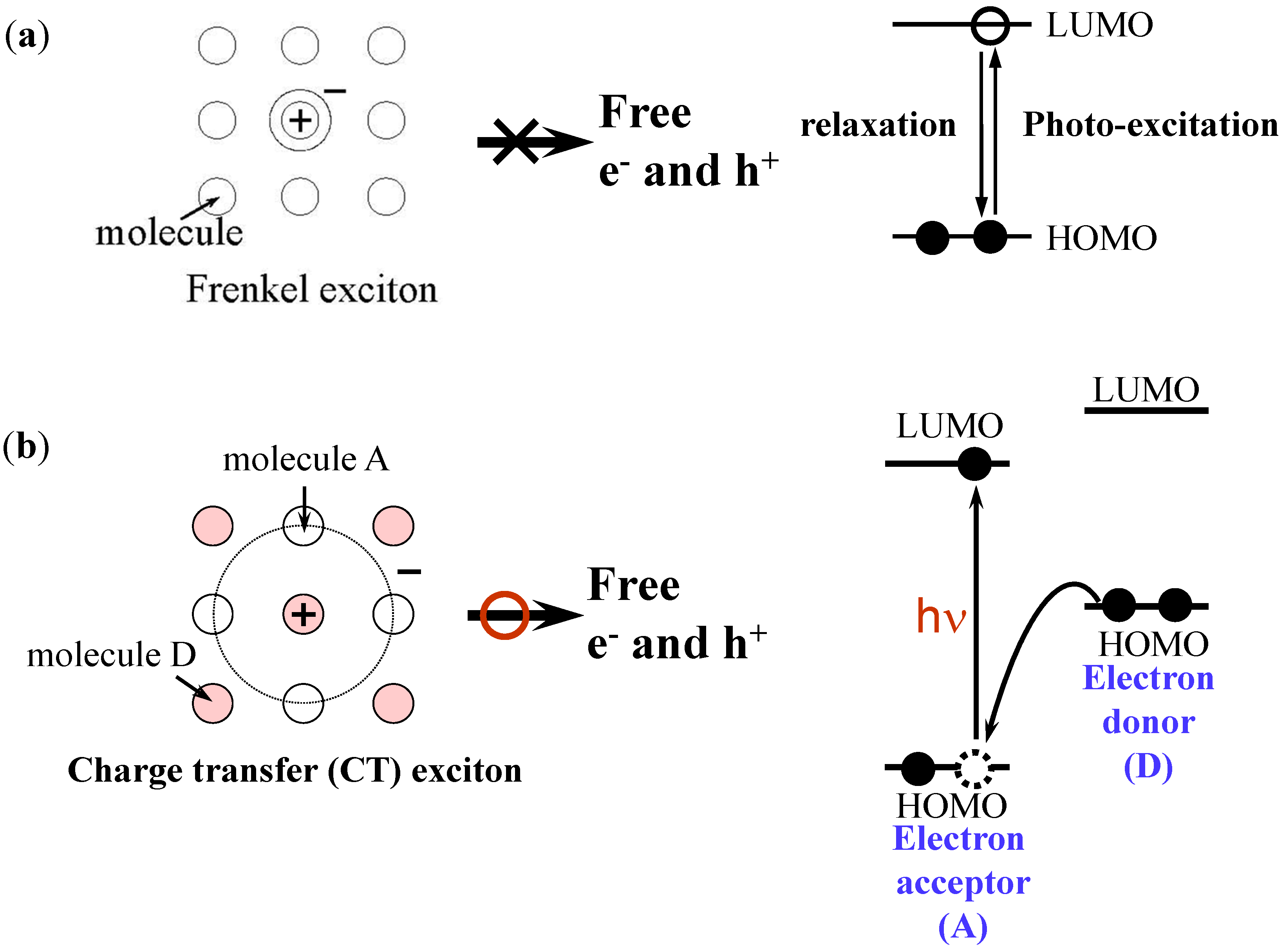
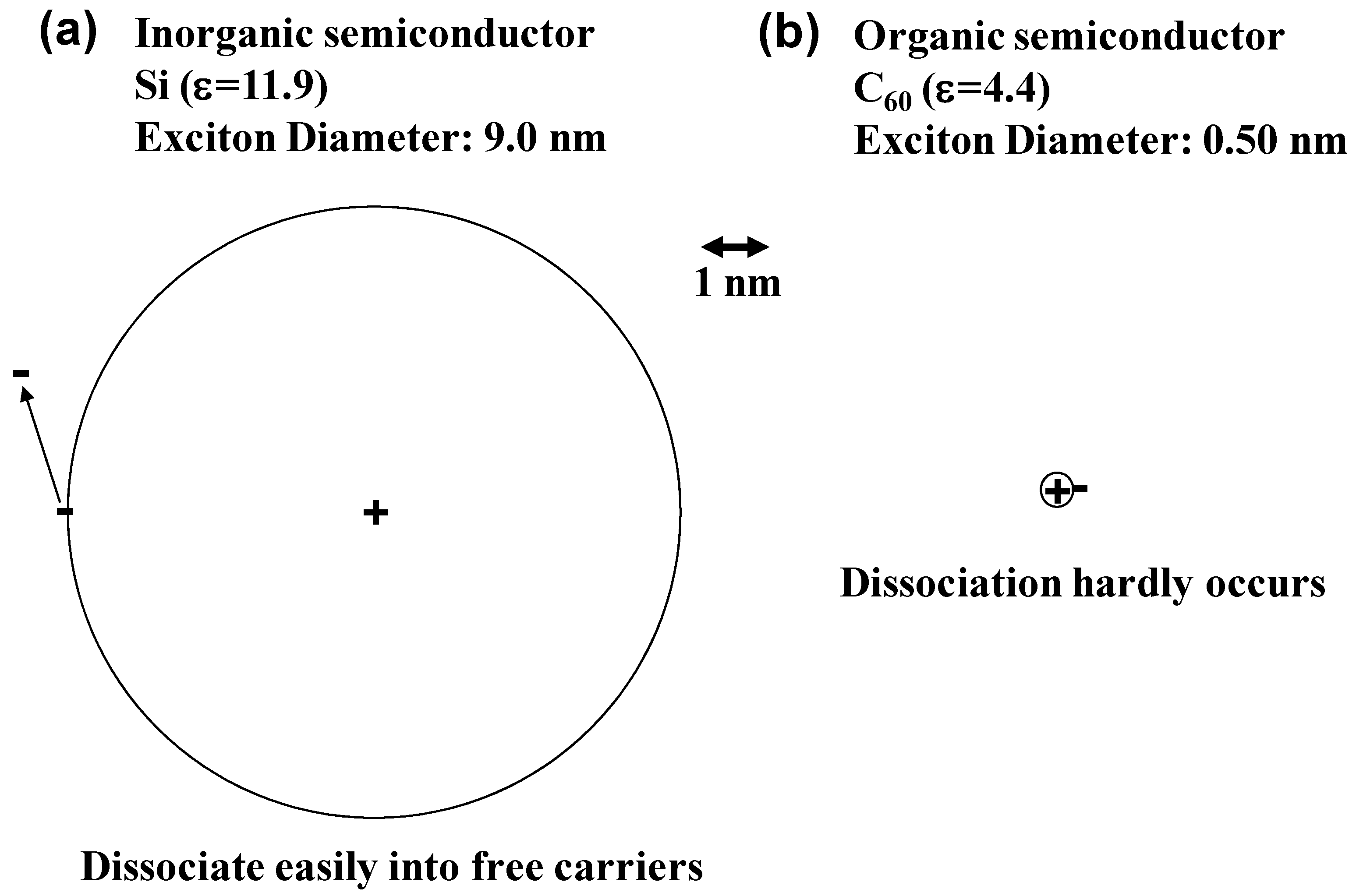
2.1. Exciton


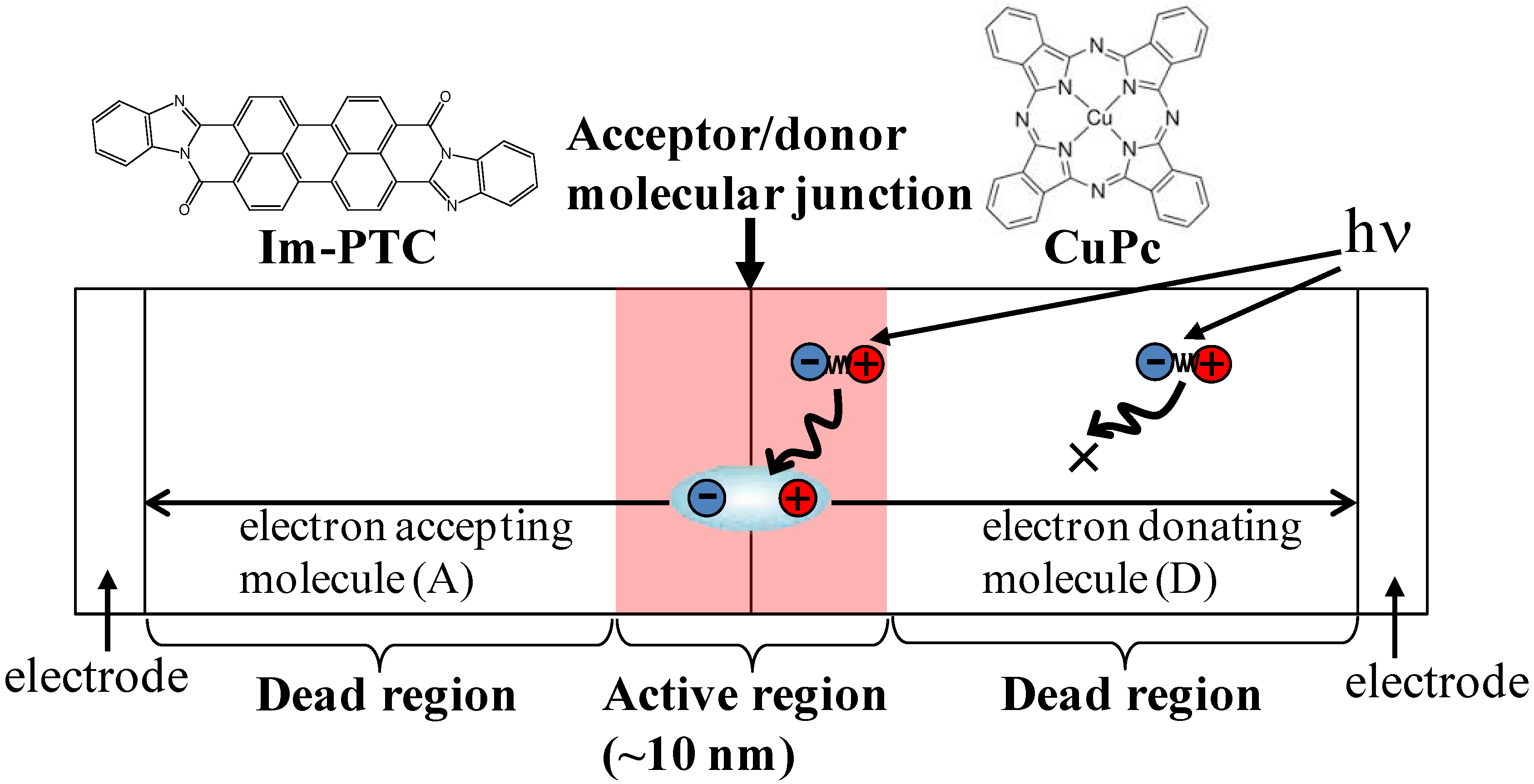
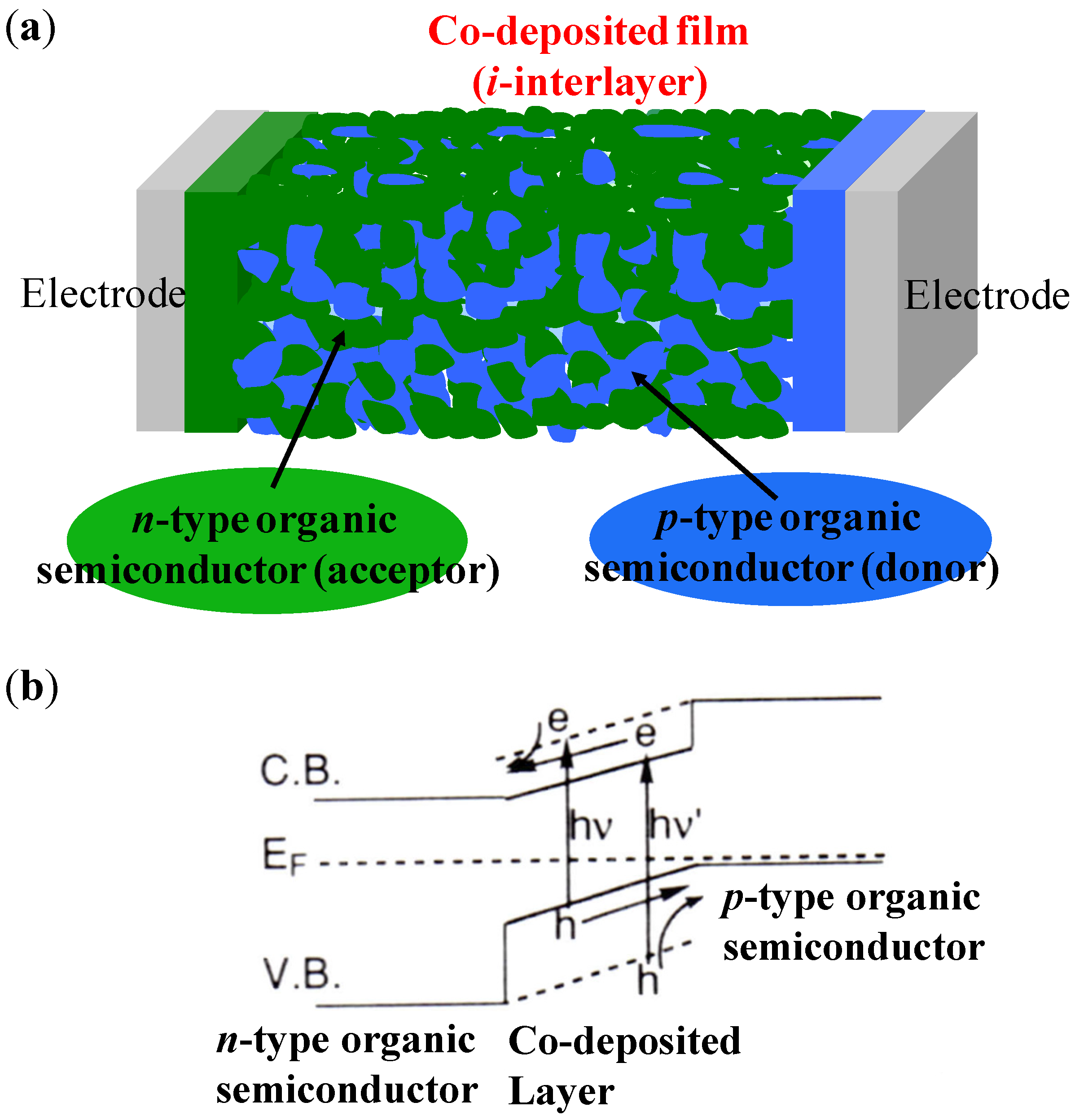
2.2. Co-Deposited Layer

3.Nanostructure Design
3.1. Vertical Superlattice Structure

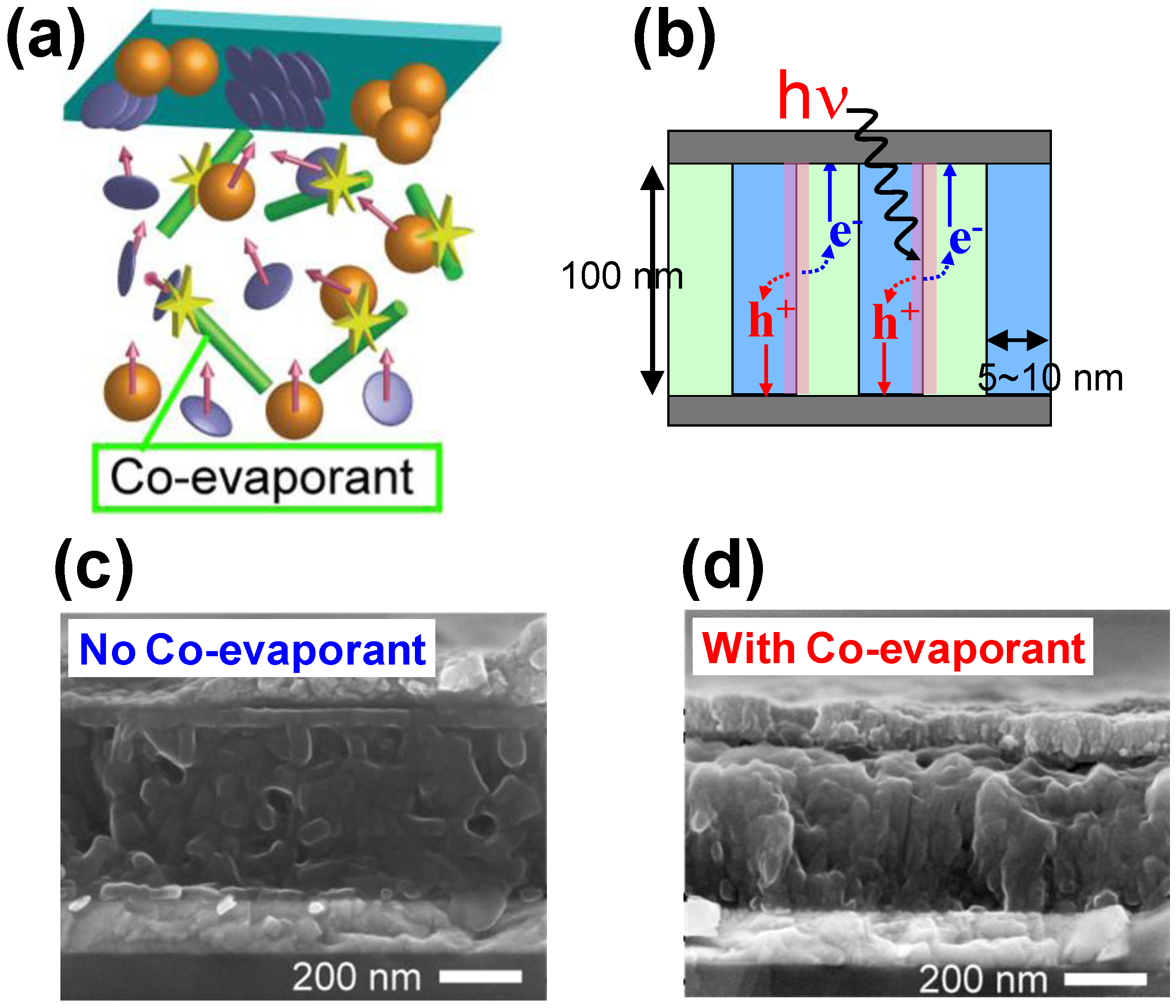
3.2. Co-Evaporant 3rd Molecules
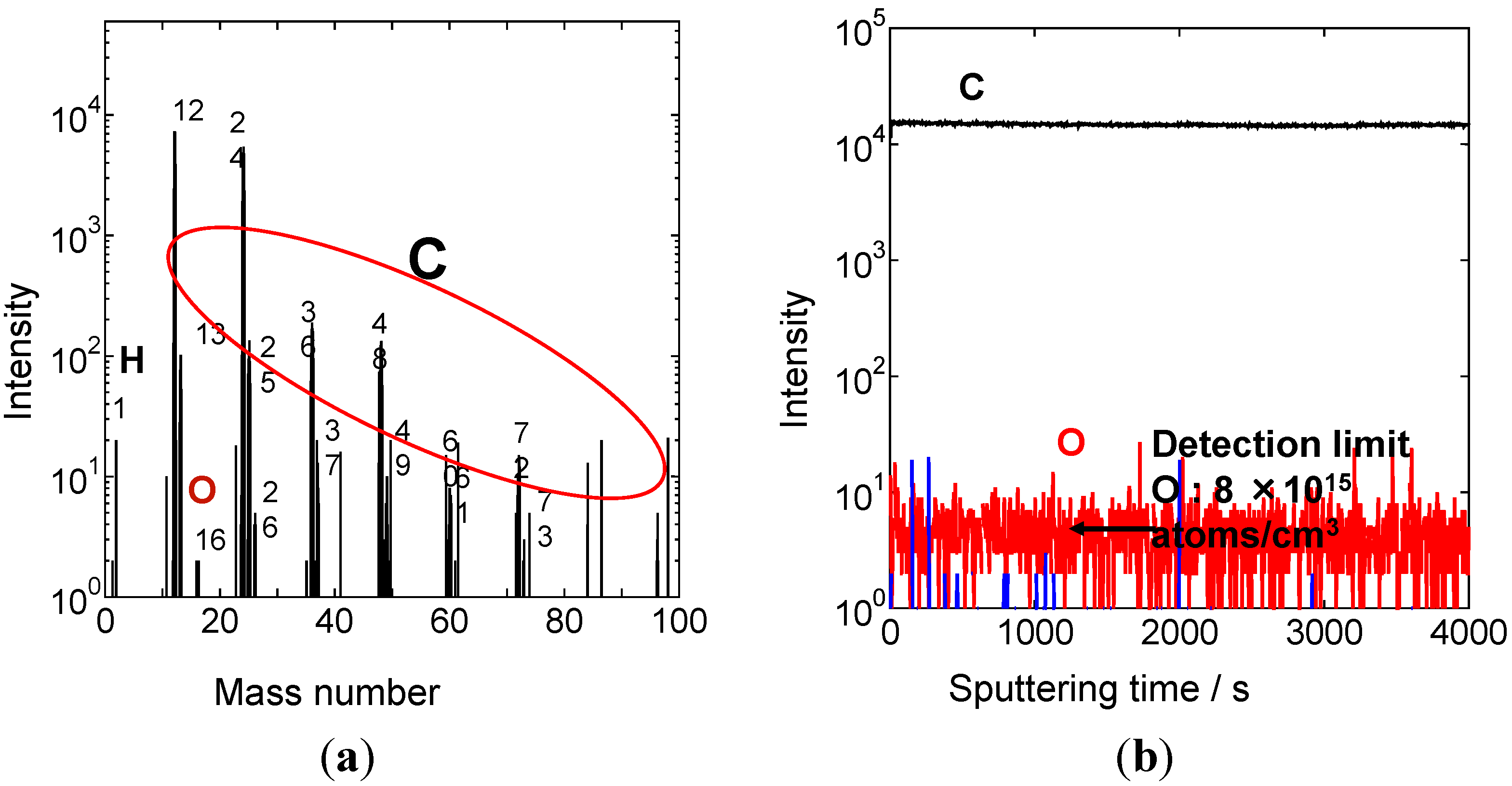
4. Seven-Nines (7N) Purification
4.1. Single-Crystal Sublimation
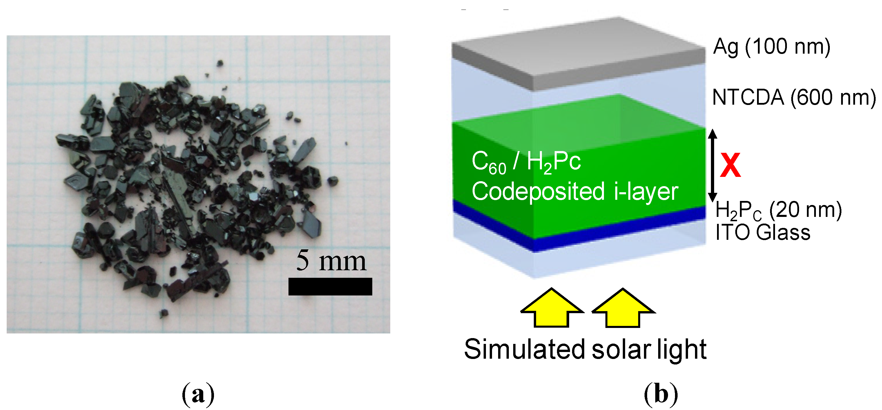
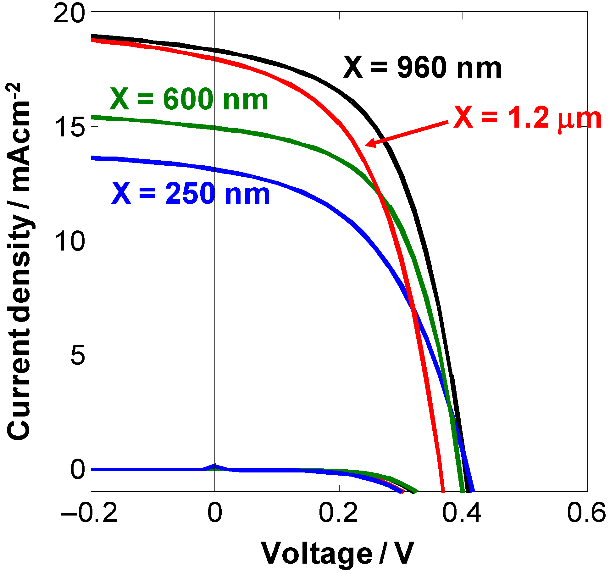
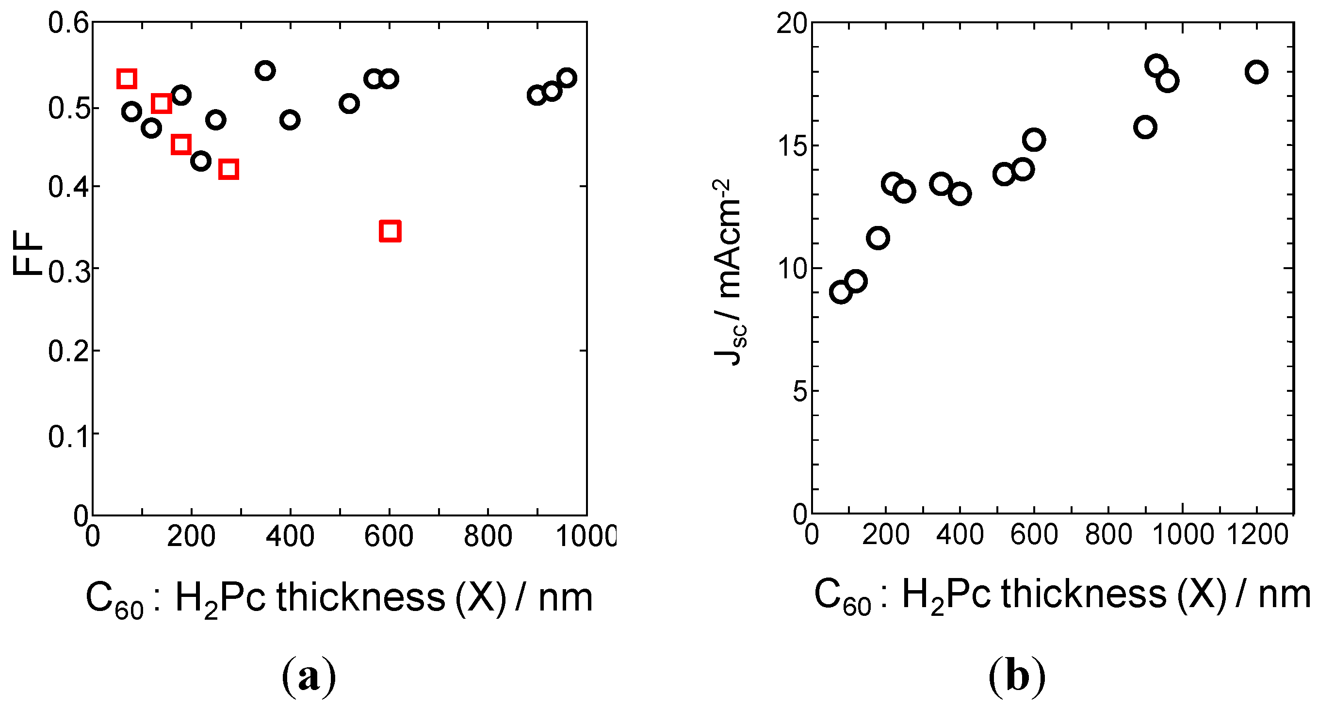
4.2. One Micrometer-Thick Co-Deposition Cells


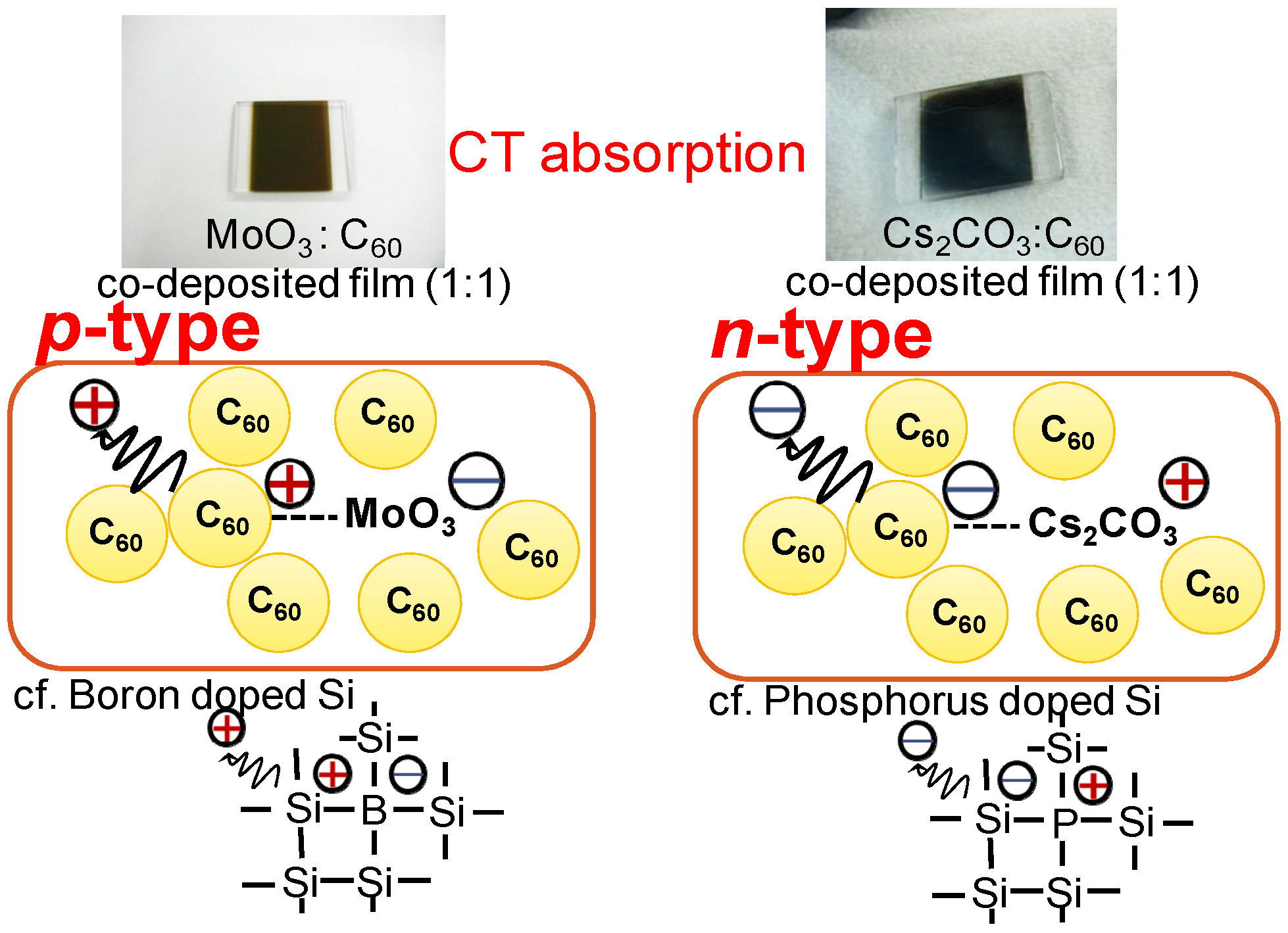
5. pn-Control by Doping
5.1. Background
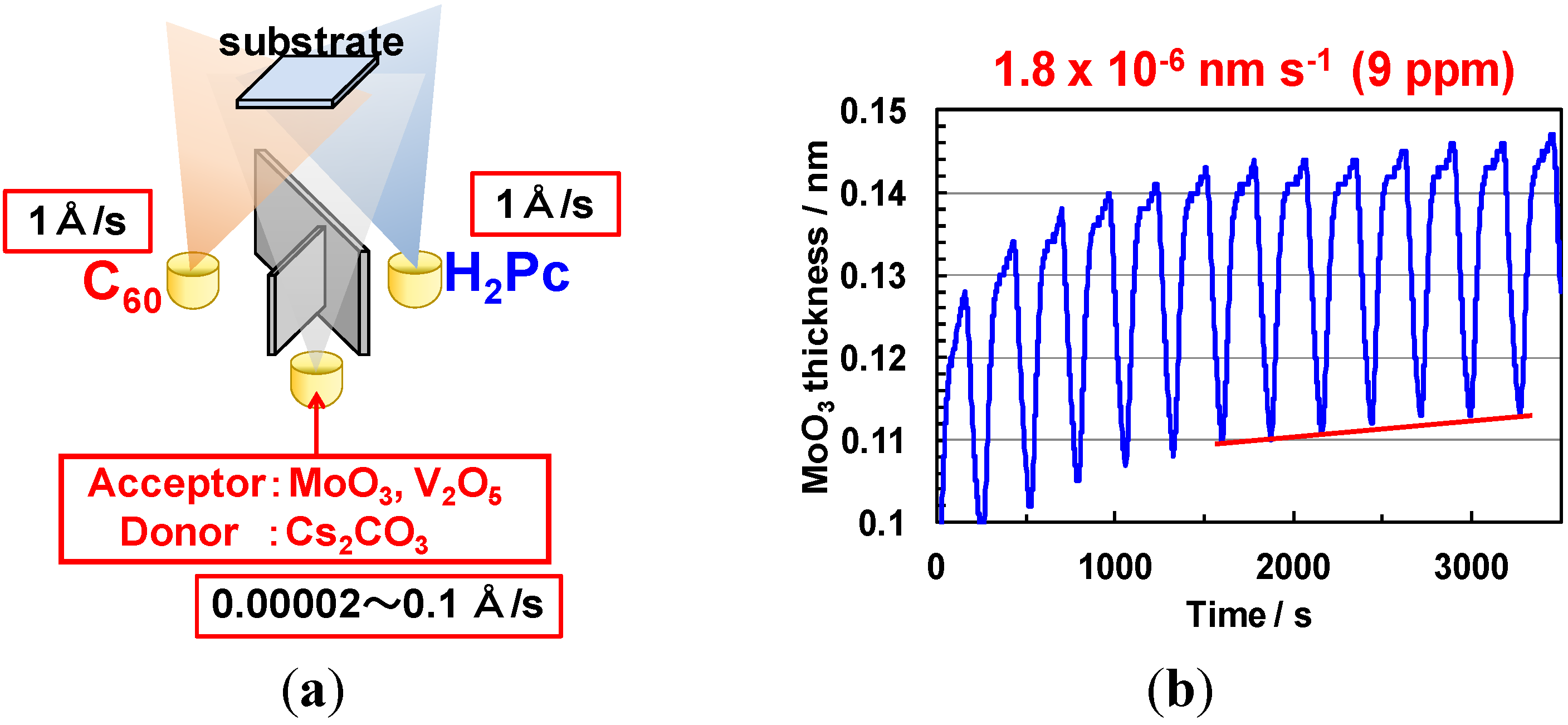
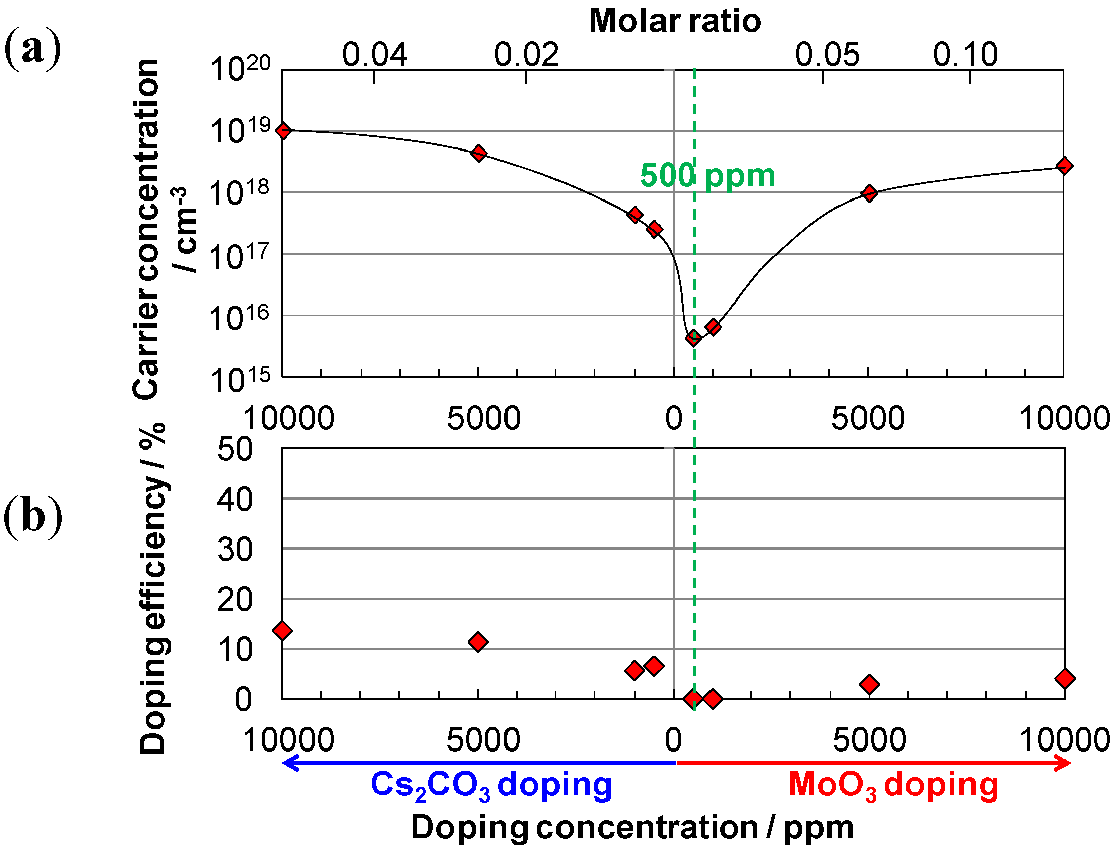
5.2. Method of ppm-Level Doping
5.3. pn-Control of Single C60 Films

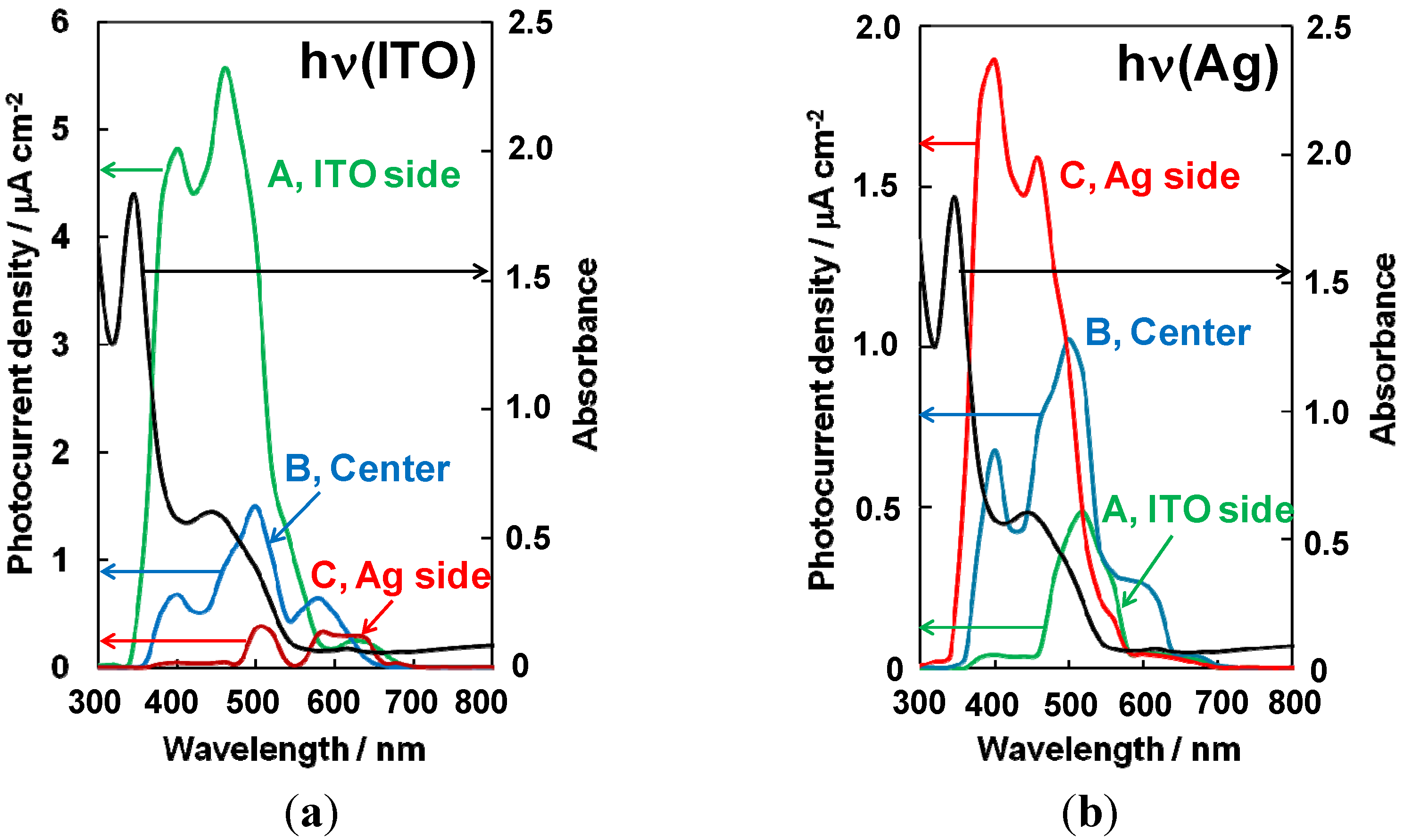
5.4. pn-Homojunction Formation in Single C60 Films


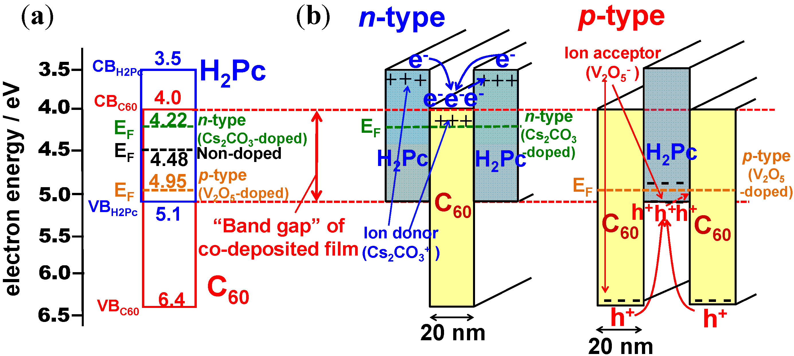
5.5. Generality
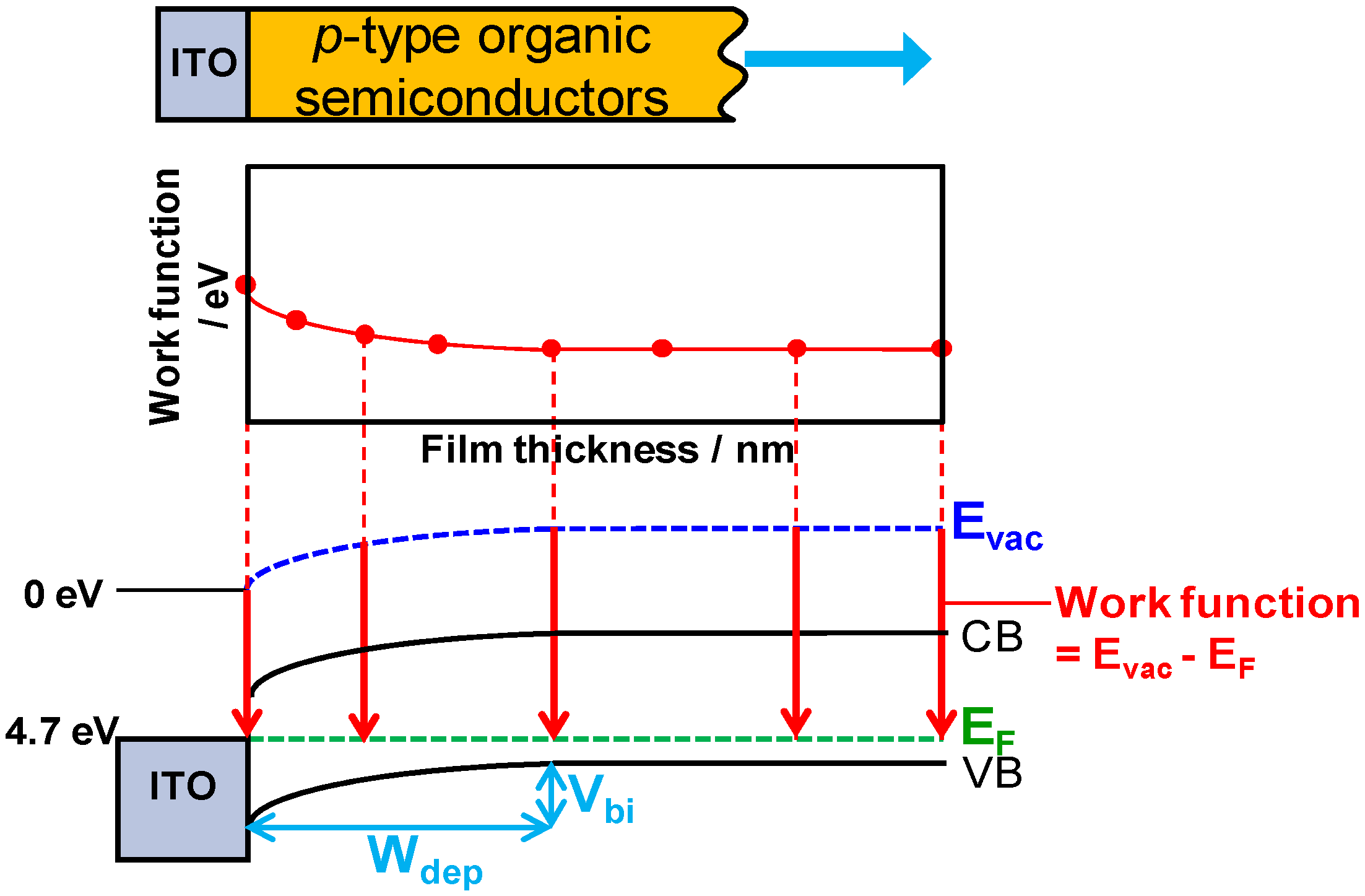
5.6. Band Mapping by Kelvin Probe


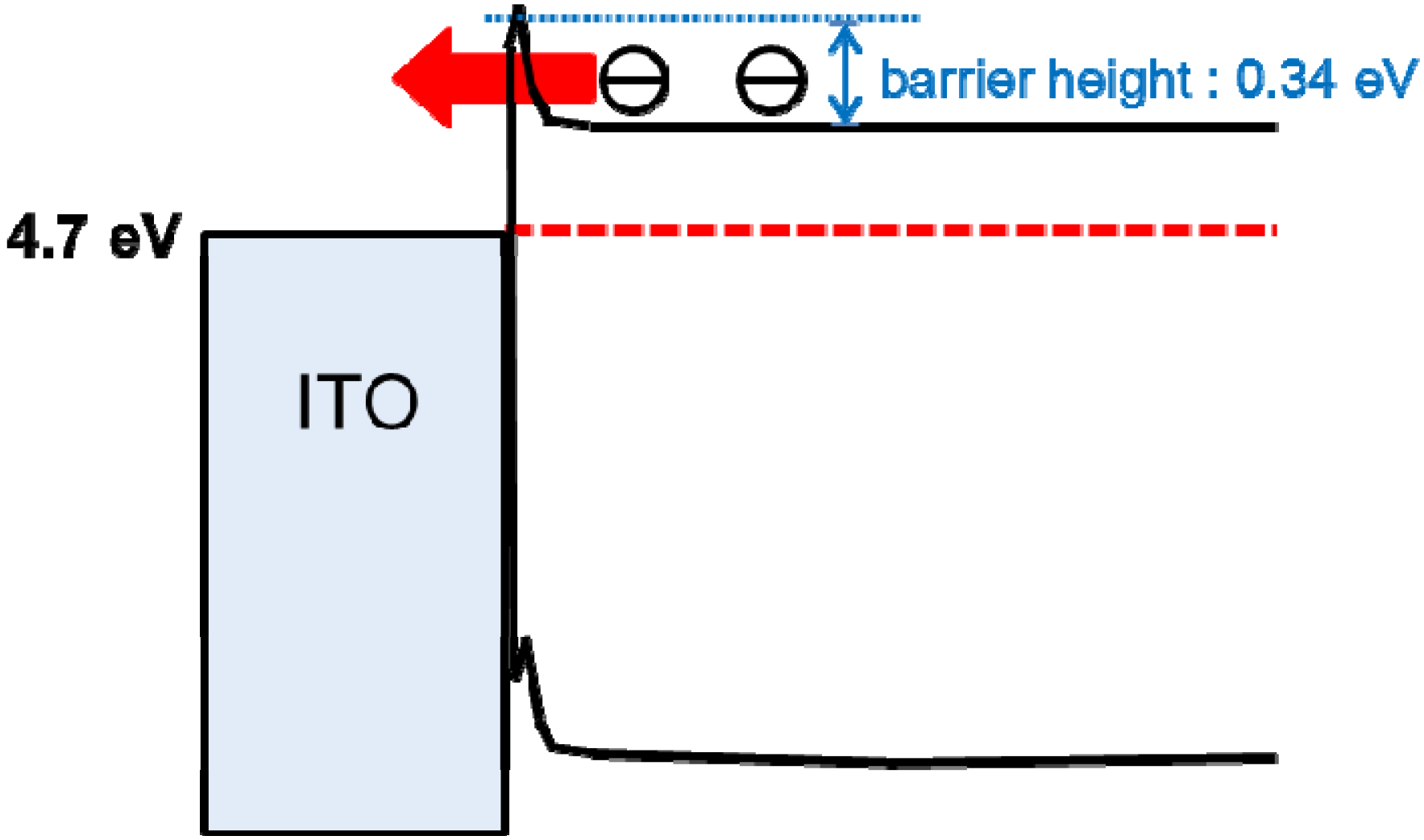
5.7. Organic/Metal Ohmic Junction

6. pn-Control of Co-deposited Films by Doping
6.1. pn-Control of Co-deposited Films
6.2. Organic/Organic Ohmic Junction

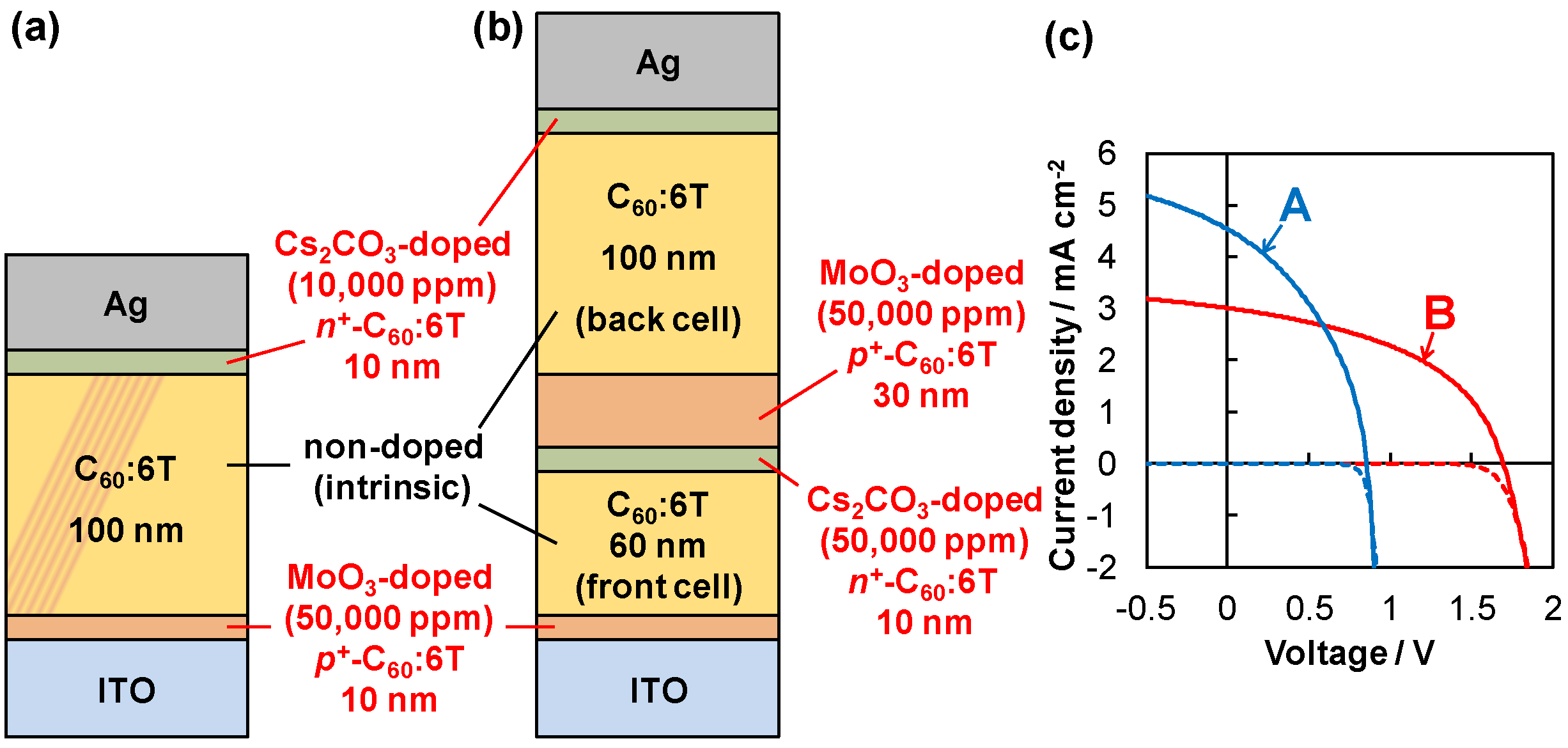
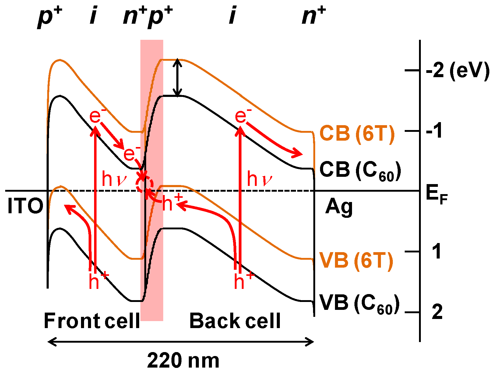
6.3. Tandem Cells Formed in Co-Deposited Films by Doping

7. Conclusions
Acknowledgments
Conflicts of Interest
References and Notes
- Organic Photovoltaics, Mechanisms, Materials and Devices; Sun, S.-S.; Sariciftci, N.S. (Eds.) CRC Press: New York, NY, USA, 2005.
- Spanggaard, H.; Krebs, F.C. A brief history of the development of organic and polymeric photovoltaics. Sol. Energy Mater. Sol. Cells 2004, 83, 125–146. [Google Scholar] [CrossRef]
- Hoppe, H.; Sariciftci, N.S. Organic solar cells: An overview. J. Mater. Res. 2004, 19, 1924–1945. [Google Scholar] [CrossRef]
- Tang, C.W. Two-layer organic photovoltaic cell. Appl. Phys. Lett. 1986, 48, 183–185. [Google Scholar] [CrossRef]
- Hiramoto, M.; Fujiwara, H.; Yokoyama, M. Three-layered organic solar cell with a photoactive interlayer of codeposited pigments. Appl. Phys. Lett. 1991, 58, 1062–1064. [Google Scholar] [CrossRef]
- Hiramoto, M.; Fujiwara, H.; Yokoyama, M. p-i-n like behavior in three-layered organic solar cells having a co-deposited interlayer of pigments. J. Appl. Phys. 1992, 72, 3781–3787. [Google Scholar] [CrossRef]
- Yu, G.; Gao, J.; Hummelen, J.C.; Wudl, F.; Heeger, A.J. Polymer photovoltaic cells: Enhanced efficiencies via a network if internal donor-acceptor heterojunctions. Science, 1995; 270, 1789–1791. [Google Scholar]
- Note: Precisely, since the exciton, i.e., the bound electron-hole pair, resembles the hydrogen atom, quantized description is needed. Rydberg levels based on the Bohr’s model of hydrogen atom can be expressed by the following equation; E = EG – G/n2 (n = 1, 2, …). (EG: Ionization energy of the molecule in the solid. G: The exciton binding energy.) The exciton binding energy (G) is proportional to µ/mε. (µ: Reduced mass of exciton. m: Mass of electron. ε: Relative permittivity.) Thus, the exciton binding energy becomes large in the organic semiconductor having small value of ε.
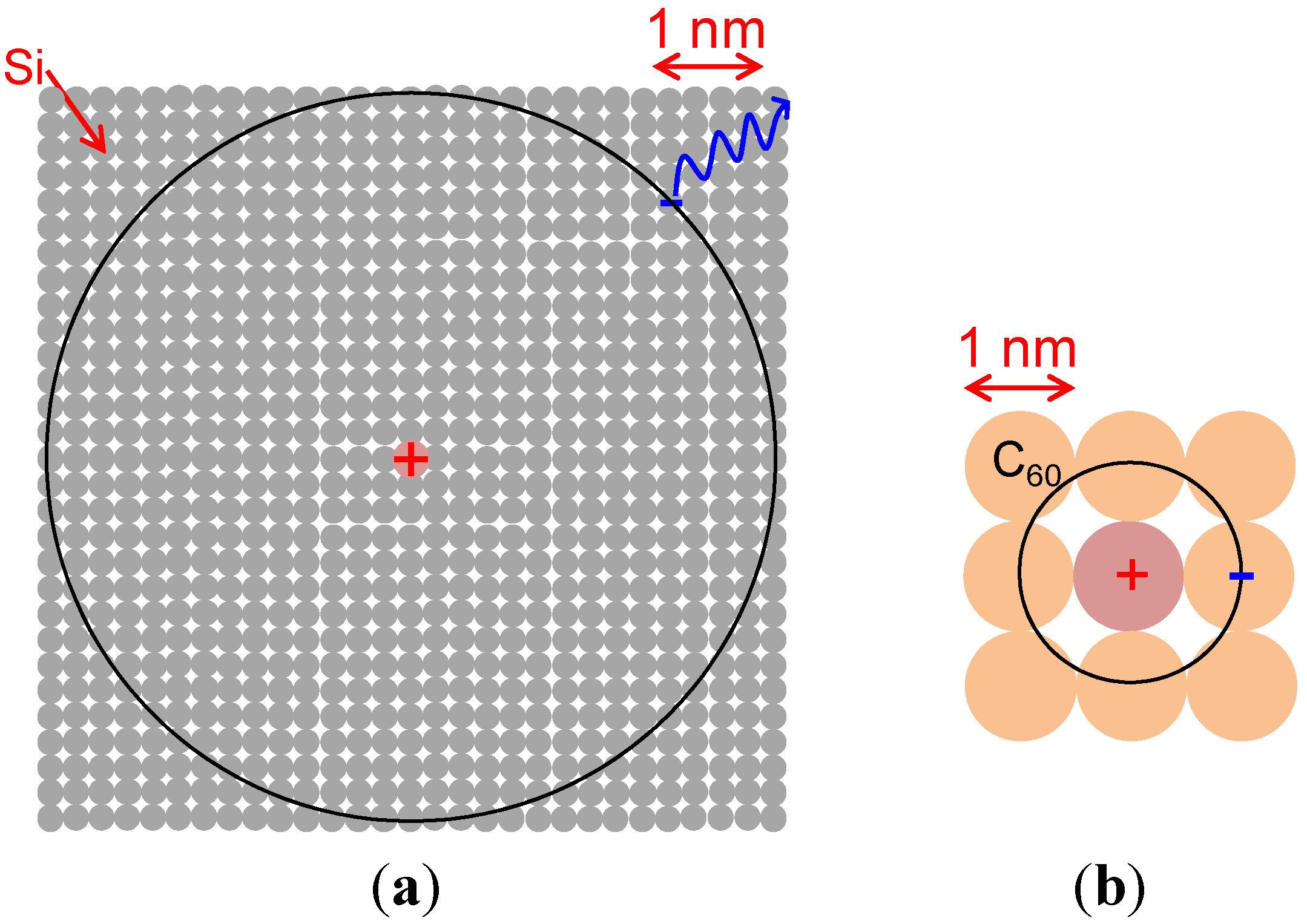
- Note: Exciton radius can be calculated based on the equation expressing the Bohr radius (r) including the relative permittivity (ε) and the reduced mass (m*) between the effective mass of an electron (mn*) and a hole (mp*), i.e., r = ε0εh2/πm*e2. Values of m* are 0.14 and 0.94 for Si and C60, respectively.
- Peumans, P.; Yakimov, A.; Forrest, S.R. Small molecular weight organic thin-film photodetectors and solar cells. J. Appl. Phys. 2003, 93, 3693–3723. [Google Scholar] [CrossRef]
- Hiramoto, M.; Yamaga, T.; Danno, M.; Suemori, K.; Matsumura, Y.; Yokoyama, M. Design of nanostructure for photoelectric conversion using an organic vertical superlattice. Appl. Phys. Lett. 2006, 88, 213105. [Google Scholar] [CrossRef]
- Kaji, T.; Zhang, M.; Nakao, S.; Iketaki, K.; Yokoyama, K.; Tang, C.W.; Hiramoto, M. Co-evaporant induced crystalline donor:acceptor blends in organic solar cells. Adv. Mat. 2011, 23, 3320–3325. [Google Scholar] [CrossRef]
- Matsuo, Y.; Sato, Y.; Niinomi, T.; Soga, I.; Tanaka, H.; Nakamura, E. Columnar structure in bulk heterojunction in solution-processable three-layered p-i-n organic photovoltaic devices using tetrabenzoporphyrin precursor and silylmethyl[60]fullerene. J. Am. Chem. Soc. 2009, 131, 16048–16050. [Google Scholar]
- Wagner, H.J.; Loutfy, R.O.; Hsiao, C. Purification and characterization of phthalocyanines. J. Mater. Sci. 1982, 17, 2781–2791. [Google Scholar] [CrossRef]
- Laudise, R.A.; Kloc, Ch.; Simpkins, P.G.; Siegrist, T. Physical vapor growth of organic semiconductors. J. Cryst. Growth 1998, 187, 449–454. [Google Scholar] [CrossRef]
- Suemori, K.; Miyata, T.; Yokoyama, M.; Hiramoto, M. Organic solar cells protected by very thick naphthalene tetracarboxylic anhydride films. Appl. Phys. Lett. 2004, 85, 6269–6271. [Google Scholar]
- Surmori, K.; Yokoyama, M.; Hiramoto, M. Electrical shorting of organic photovoltaic films resulting from metal migration. J. Appl. Phys. 2006, 99, 036109. [Google Scholar] [CrossRef]
- Suemori, K.; Miyata, T.; Yokoyama, M.; Hiramoto, M. Three-layered organic solar cells incorporating nanostructure-optimized Phthalocyanine:Fullerene codeposited interlayer. Appl. Phys. Lett. 2005, 86, 063509. [Google Scholar] [CrossRef]
- Sakai, K.; Hiramoto, M. Efficient organic p-i-n solar cells having very thick codeposited i-layer consisting of highly purified organic semiconductors. Mol. Cryst. Liq. Cryst. 2008, 491, 284–289. [Google Scholar] [CrossRef]
- Hiramoto, M. Efficient organic p-i-n solar cells having very thick codeposited i-layer composed of highly purified organic semiconductors. Proc. SPIE 2008, 7052. [Google Scholar] [CrossRef]
- Note: Thick NTCDA protection against electrical shorting is no longer needed since the i-layer has sufficient thickness. So, we could replace NTCDA (600 nm) with C60 (80 nm)/bathocuproine (BCP; 15 nm) or C60 (80 nm)/NTCDA (80 nm)/bathocuproine (BCP; 15 nm) and obtain similar results. For the latter case, cell parameters are Jsc: 17.5 mAcm−2, Voc: 0.44 V, FF: 0.57, efficiency: 5.3% (81.8 mWcm−2).
- Brenninghoven, A.; Rundenauer, F.G.; Werner, H.W. Secondary Ion Mass Spectrometry; John Wiley & Sons: New York, NY, USA, 1987. [Google Scholar]
- Note: Purity of 7N was also confirmed by temperature programmed desorption mass spectroscopy.
- Tanaka, Y.; Kanai, K.; Ouchi, Y.; Seki, K. Oxygen effect on the interfacial electronic structure of C60 film studied by ultraviolet photoelectron spectroscopy. Chem. Phys. Lett. 2007, 441, 63–67. [Google Scholar] [CrossRef]
- Martin, M.; Andre, J.-J.; Simon, J. Influence of dioxygen on the junction properties of metallophthalocyanine based devices. J. Appl. Phys. 1983, 54, 2792–2794. [Google Scholar] [CrossRef]
- Tada, H.; Touda, H.; Takada, M.; Matsushige, K. Quasi-intrinsic semiconducting state of titanyl-phthalocyanine films obtained under ultrahigh vacuum conditions. Appl. Phys. Lett. 2000, 76, 873–875. [Google Scholar] [CrossRef] [Green Version]
- Akamatsu, H.; Inokuchi, H.; Matsunaga, Y. Electrical conductivity of the perylene-bromine complex. Nature 1954, 173, 168–169. [Google Scholar] [CrossRef]
- Hiramoto, M.; Ihara, K.; Fukusumi, H.; Yokoyama, M. Conduction type control from n- to p-type for organic pigment film purified by reactive sublimation. J. Appl. Phys. 1995, 78, 7153–7157. [Google Scholar] [CrossRef]
- Hiramoto, M.; Ihara, K.; Yokoyama, M. Fermi level shift in photoconductive organic pigment films measured by Kelvin vibrating capacitor method. Jpn. J. Appl. Phys. 1995, 34, 3803–3807. [Google Scholar] [CrossRef]
- Huang, J.S.; Pfeiffer, M.; Werner, A.; Blochwitz, J.; Leo, K.; Liu, S.Y. Low-voltage organic electroluminescent devices using pin structures. Appl. Phys. Lett. 2002, 80, 139–141. [Google Scholar] [CrossRef]
- Blochwitz, J.; Pfeiffer, M.; Fritz, T.; Leo, K. Low voltage organic light emitting diodes featuring doped phthalocyanine as hole transport material. Appl. Phys. Lett. 1998, 73, 729–731. [Google Scholar] [CrossRef]
- Tokito, S.; Noda, K.; Taga, Y. Metal oxides as a hole-injecting layer for an organic electroluminescent device. J. Phys. D 1996, 29, 2750–2753. [Google Scholar] [CrossRef]
- Matsushima, T.; Kinoshita, Y.; Murata, H. Formation of Ohmic hole injection by inserting an ultrathin layer of molybdenum trioxide between indium tin oxide and organic hole-transporting layers. Appl. Phys. Lett. 2007, 91, 253504:1–253504:3. [Google Scholar]
- Harada, K.; Werner, A.G.; Pfeiffer, M.; Bloom, C.J.; Elliott, C.M.; Leo, K. Organic homojunction diodes with a high built-in potential: interpretation of the current-voltage characteristics by a generalized einstein relation. Phys. Rev. Lett. 2005, 94, 036601:1–036601:4. [Google Scholar]
- Chan, C.K.; Zhao, W.; Barlow, S.; Marder, S.; Kahn, A. Decamethylcobaltocene as an efficient n-dopant in organic electronic materials and devices. Org. Electron. 2008, 9, 575–581. [Google Scholar] [CrossRef]
- Harada, K.; Riede, M.; Leo, K. Pentacene homojunctions: Electron and hole transport properties and related photovoltaic responses. Phys. Rev. B 2008, 77, 195212:1–195212:9. [Google Scholar]
- Liao, H.-H.; Chen, L.-M.; Xu, Z.; Li, G.; Yang, Y. Highly efficient inverted polymer solar cell by low temperature annealing of Cs2CO3 interlayer. Appl. Phys. Lett. 2008, 92, 173303. [Google Scholar] [CrossRef]
- Hamwi, S.; Riedl, T.; Kowalsky, W. An organic p-i-n homojunction as ultra violet light emitting diode and visible-blind photodiode in one. Appl. Phys. Lett. 2011, 99, 053301:1–053301:3. [Google Scholar]
- Chan, C.K.; Amy, F.; Zhang, Q.; Barlow, S.; Marder, S.; Kahn, A. N-type doping of an electron-transport material by controlled gas-phase incorporation of cobaltocene. Chem. Phys. Lett. 2006, 431, 67–71. [Google Scholar] [CrossRef]
- Walzer, K.; Maennig, B.; Pfeiffer, M.; Leo, K. Highly efficient organic devices based on electrically doped transport layers. Chem. Rev. 2007, 107, 1233–1271. [Google Scholar] [CrossRef]
- Falkenberg, C.; Uhrich, C.; Olthof, S.; Maennig, B.; Riede, M.; Leo, K. Efficient p-i-n type organic solar cells incorporating 1,4,5,8-naphthalenetetracarboxylic dianhydride as transparent electron transport material. J. Appl. Phys. 2008, 104, 034506:1–034506:6. [Google Scholar]
- Yoshida, H. Low-energy inverse photoemission spectroscopy using a high-resolution grating spectrometer in the near ultraviolet range. Rev. Sci. Instrum. 2013, 84, 103901:1–103901:5. [Google Scholar] [CrossRef] [Green Version]
- Kubo, M.; Iketaki, K.; Kaji, T.; Hiramoto, M. Conduction type control of fullerene films from n- to p-type by molybdenum oxide doping. Appl. Phys. Lett. 2011, 98, 073311:1–073311:3. [Google Scholar]
- Kubo, M.; Kaji, T.; Hiramoto, M. pn-homojunction formation in single fullerene films. AIP Adv. 2011, 1, 032177:1–032177:5. [Google Scholar]
- Ishiyama, N.; Ishiyama, K.; Kubo, M.; Kaji, T.; Hiramoto, M. Tandem photovoltaic cells formed in single fullerene films by impurity doping. Appl. Phys. Lett. 2012, 101, 233303:1–233303:3. [Google Scholar]
- Shinmura, Y.; Kubo, M.; Ishiyama, N.; Kaji, T.; Hiramoto, M. pn-control and pn-homojunction formation of metal-free phthalocyanine by doping. AIP Adv. 2012, 2, 032145:1–032145:6. [Google Scholar]
- Hamwi, S.; Meyer, J.; Winkler, T.; Riedl, T.; Kowalsky, W. p-type doping efficiency of MoO3 in organic hole transport materials. Appl. Phys. Lett. 2009, 94, 253307:1–253307:3. [Google Scholar]
- Ishiyama, N.; Kubo, M.; Kaji, T.; Hiramoto, M. Doping-based control of the energetic structure of photovoltaic co-deposited films. Appl. Phys. Lett. 2011, 99, 133301:1–133301:3. [Google Scholar]
- Note: Hole concentration created by MoO3-doping (5000 ppm) was cross-checked by capacitance-voltage measurements. Obtained value of 5 × 1017 cm−3 was consistent with that measured by Kelvin method (9.6 × 1017 cm−3).
- Hebard, A.F.; Hadon, R.C.; Fleming, R.M.; Kortan, A.R. Deposition and characterization of fullerene films. Appl. Phys. Lett. 1991, 59, 2109–2111. [Google Scholar] [CrossRef]
- Note: There is no evidence of Cs2CO3 dissociation during vacuum evaporation, since a single Cs2CO3 film is completely transparent.
- Note: The radius of an electron orbital around a positively ionized donor can be calculated based on the equation expressing the Bohr radius (r) including the relative permittivity (ε) and the effective mass of an electron (mn*), i.e., r = ε0εh2/πmn*e2.
- Kröger, M.; Hamwi, S.; Meyer, J.; Riedl, T.; Kowalsky, W.; Kahn, A. P-type doping of organic wide band gap materials by transition metal oxides: A case-study on Molybdenum trioxide. Org. Electron. 2009, 10, 932–938. [Google Scholar] [CrossRef]
- deMello, J.C.; Tessler, N.; Graham, S.C.; Friend, R.H. Ionic space-charge effects in polymer light-emitting diodes. Phys. Rev. B 1998, 57, 12951–12963. [Google Scholar] [CrossRef]
- Hiramoto, M.; Tomioka, A.; Suemori, K.; Yokoyama, M. Formation of ohmic contacts to perylene molecular crystals. Appl. Phys. Lett. 2004, 85, 1852–1854. [Google Scholar] [CrossRef]
- Kubo, M.; Shinmura, Y.; Ishiyama, N.; Kaji, T.; Hiramoto, M. Invertible organic photovoltaic cells with heavily-doped organic/metal ohmic contacts. Appl. Phys. Expr. 2012, 5, 092302:1–092302:3. [Google Scholar]
- Note: The inverse photovoltaic effect in Figure 22(d)(blue curve) can be attributed to the p-type Schottky junction formation at Ag/H2Pc interface. Absence of C60 sensitivity of action spectrum of Jsc of inverse photocurrent showed that the inverse photocurrent was generated near H2Pc/Ag electrode.
- Kubo, M.; Kaji, T.; Hiramoto, M. pn-homojunction organic solar cells formed in the thick phase-separated co-deposited films by doping. Appl. Phys. Lett. 2013, 103, 263303:1–263303:4. [Google Scholar]
- Kubo, M.; Shinmura, Y.; Ishiyama, N.; Kaji, T.; Hiramoto, M. Junction formation by doping in H2Pc:C60 co-evaporated films for solar cell application. Mol. Cryst. Liq. Cryst. 2013, 581, 13–17. [Google Scholar] [CrossRef]
- Ishiyama, N.; Kubo, M.; Kaji, T.; Hiramoto, M. Tandem organic solar cells formed in co-deposited films by doping. Org. Electron. 2013, 14, 1793–1796. [Google Scholar] [CrossRef]
- Hiramoto, M.; Suezaki, M.; Yokoyama, M. Effect of thin gold interstitial-layer on the photovoltaic properties of tandem organic solar cell. Chem. Lett. 1990, 327–330. [Google Scholar] [CrossRef]
- Yuan, Y.; Huang, J.; Li, G. Intermediate layers in tandem organic solar cells. Green 2011, 1, 65–80. [Google Scholar]
© 2014 by the authors; licensee MDPI, Basel, Switzerland. This article is an open access article distributed under the terms and conditions of the Creative Commons Attribution license (http://creativecommons.org/licenses/by/3.0/).
Share and Cite
Hiramoto, M.; Kubo, M.; Shinmura, Y.; Ishiyama, N.; Kaji, T.; Sakai, K.; Ohno, T.; Izaki, M. Bandgap Science for Organic Solar Cells. Electronics 2014, 3, 351-380. https://doi.org/10.3390/electronics3020351
Hiramoto M, Kubo M, Shinmura Y, Ishiyama N, Kaji T, Sakai K, Ohno T, Izaki M. Bandgap Science for Organic Solar Cells. Electronics. 2014; 3(2):351-380. https://doi.org/10.3390/electronics3020351
Chicago/Turabian StyleHiramoto, Masahiro, Masayuki Kubo, Yusuke Shinmura, Norihiro Ishiyama, Toshihiko Kaji, Kazuya Sakai, Toshinobu Ohno, and Masanobu Izaki. 2014. "Bandgap Science for Organic Solar Cells" Electronics 3, no. 2: 351-380. https://doi.org/10.3390/electronics3020351