Review

Bio-Organic Electronics—Overview and Prospects for the Future

Fraunhofer Institute for Electron Beam, Plasma Technology and COMEDD (FEP), Maria-Reiche-Str. 02, 01109 Dresden, Germany
*
Author to whom correspondence should be addressed.
Electronics 2014, 3(3), 444-461; https://doi.org/10.3390/electronics3030444
Submission received: 8 March 2014 / Revised: 10 June 2014 / Accepted: 7 July 2014 / Published: 18 July 2014
(This article belongs to the Special Issue Organic Semiconductors)

Abstract

:
In recent years, both biodegradable and bio-based electronics have attracted increasing interest, but are also controversially discussed at the same time. Yet, it is not clear whether they will contribute to science and technology or whether they will disappear without major impact. The present review will address several aspects while showing the potential opportunities of bio-organic electronics. An overview about the complex terminology of this emerging field is given and test methods are presented which are used to evaluate the biodegradable properties. It will be shown that the majority of components of organic electronics can be substituted by biodegradable or bio-based materials. Moreover, application scenarios are presented where bio-organic materials have advantages compared to conventional ones. A variety of publications are highlighted which encompass typical organic devices like organic light emitting diodes, organic solar cells and organic thin film transistors as well as applications in the field of medicine or agriculture.

Graphical Abstract

1. Introduction

Until the 1930s, plastics were almost exclusively fabricated from regrowing resources [1]. Only since the end of the Second World War have raw material sources of non-renewable fossil materials, such as petroleum and natural gas, been generally used. However, within the last 20 years, efforts have continuously increased to enhance the share of bio-based materials in the world of plastics.
Along with the objective to improve the properties of products and to reduce the production cost of materials, the general discussion about greenhouse gases, difficulties in waste management, e.g., the Great Pacific garbage patch in the ocean, and the awareness about the limitation of fossil fuels have contributed considerably to the revived interest and increasing implementation of bio-plastics.
The following paper presents a comprehensive overview of bio-organic electronics and their potential to enable easy waste disposal. At first, essential terms are defined and correlated with standards while summarizing various testing procedures to assess the hazardous risk of potentially biodegradable electronics with regard to the environment.
The principle structure of typical organic electronics is discussed with regard to their separate components. Most progress has so far been achieved in respect to the polymer carrier substrate, which will surely foster further innovation in this novel field. Besides, impressive achievements have also been demonstrated for the charge carrier transporting organic semiconductors itself. Hence, semi or fully biodegradable devices will be presented and their performance is discussed in more detail. Finally, an outlook to the future market is given.

2. Policies and Guidelines

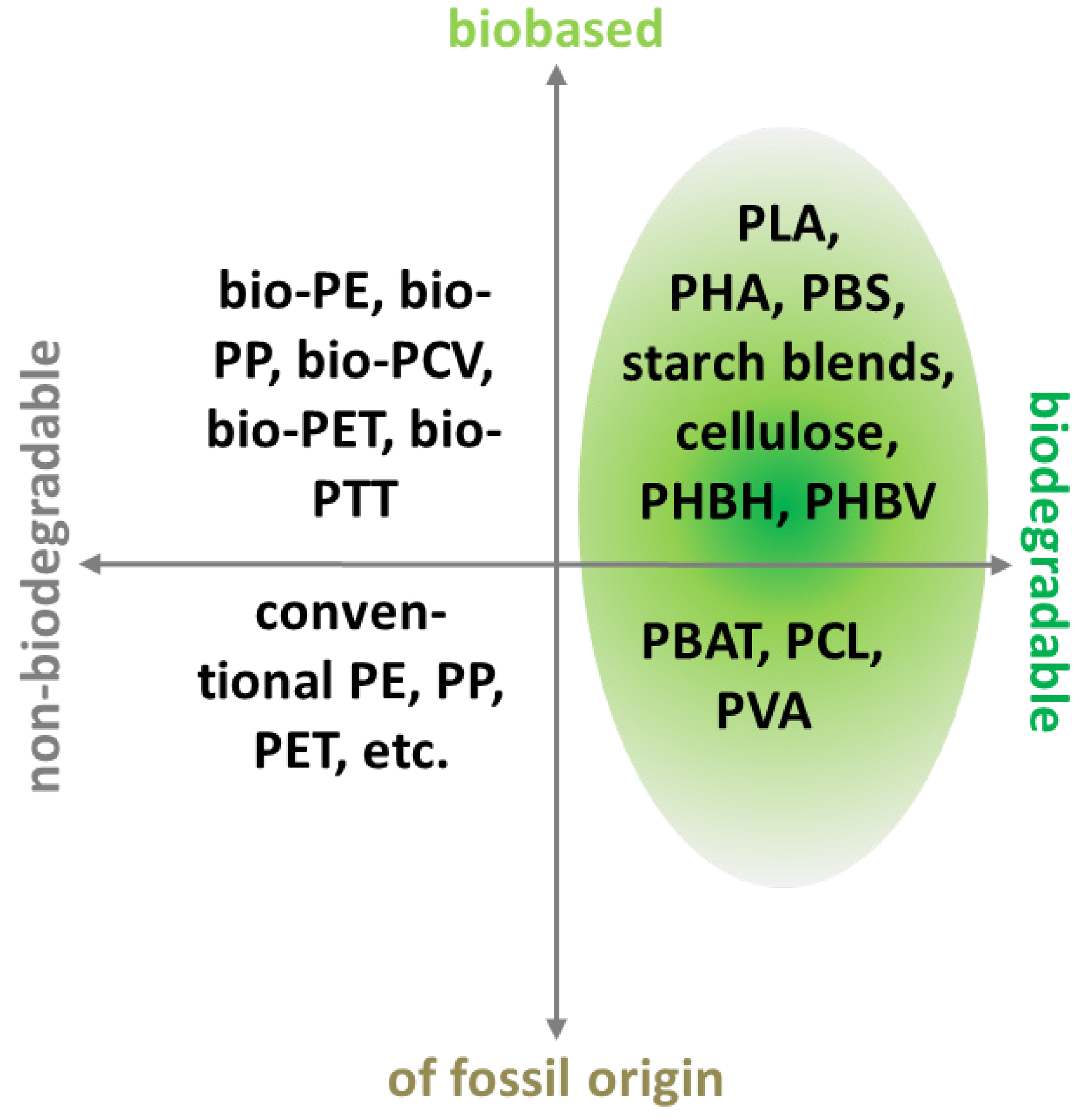
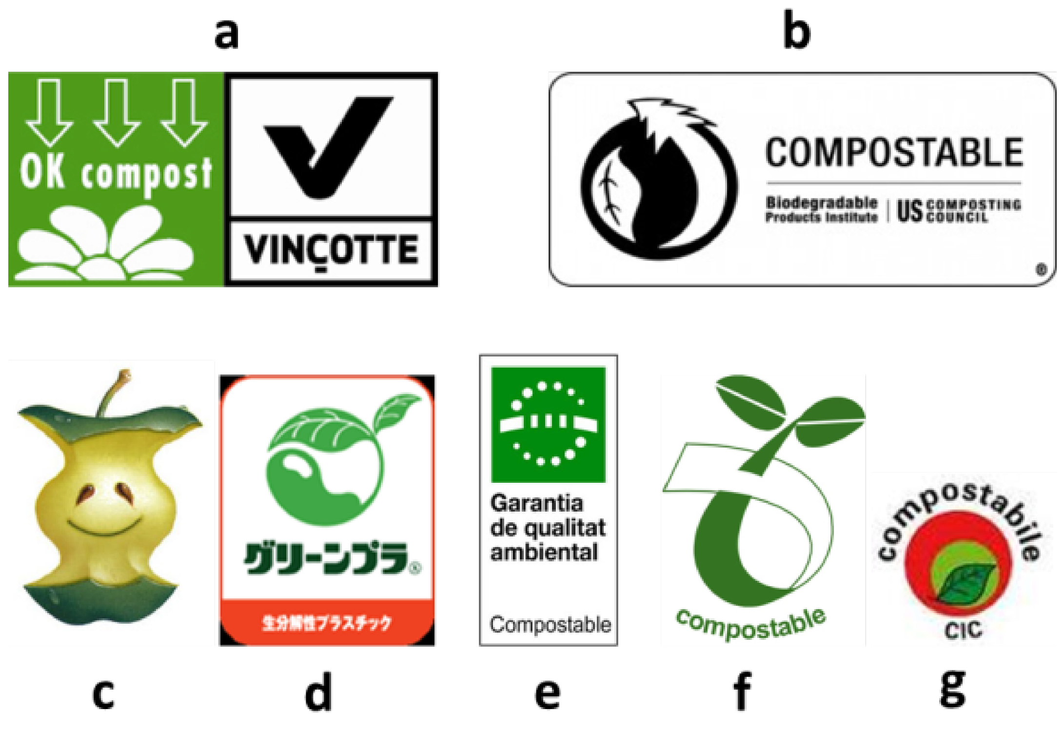
2.1. Definitions and Standards

In recent years, the syllable “bio” has become a powerful attribute to attract public attention for designated “green” processes. “Bio” is generally used in a broad context which often complicates communication between experts and beginners in this interesting field. Thus, in the following paragraph the use of these common terms shall be clarified in context to this paper.
Products are considered as bio-based when they are made of materials derived from living (or once living) organisms. Often they are denoted as biomaterials—but this term is also widely used for any interaction between biological and non-biological systems. Bio-based materials are often biodegradable with a few exceptions (mainly composites where the degradable compound is combined with non-degradable materials). The term biodegradability, however, is a more precisely certified performance characteristic. According to EN 13432, compounds are biodegradable if a share of more than 90% converts to H2O, CO2 and biomass under defined temperature, humidity, and oxygen conditions within 180 days in the presence of microorganisms or fungi. However, biodegradable plastics are not inevitably made of bio-based, renewable materials. There are several examples where fossil resources are used, and a closer look into the production volume of biodegradable materials depending on their raw material origins (Figure 1) shows that the share of both types is nearly equal. Thus, the property of biodegradability is only linked to the chemical structure and not in any way related to its origin. In nature, the biodegradation occurs either aerobically or anaerobically. In the latter process, the material is converted without oxygen to methane, CO2, H2O, energy, and biomass [2]. In the presence of oxygen (aerobic), methane is not formed.
Figure 1. Global market of bio-based/non-biodegradable (green) and biodegradable (grey) plastics in 2012 with a total volume of 1.4 million tons [3].
Electronics 03 00444 g001
Depending on the molecular weight of the compound, biodegradation begins with chain cleavage by enzymes (e.g., lipases and esterases) released by microorganisms. This mainly occurs on the surface of the biodegradable compound since the enzymes are too large to diffuse into the bulk material. After the cleavage, these fragments can be absorbed by the cells of the microorganisms. During that metabolism process, the cells can gain energy from this mineralization process [2,4].
Along with the European standard 13432, there is a variety of other standards all over the globe available (ISO 17088, ASTM D 6400 in North America, GreenPla in Japan). The ISO 17088, EN 13432 and ASTM D 6400 define the requirements concerning packaging and choice of materials being considered as “biodegradable” in industrial composting facilities. If a material passes the tests necessary to achieve this status, additional tests might be necessary to get the final product registration according to ISO 17088. After this procedure has been applied, it ensures that nonconforming, potentially toxic additives, colors and package goods are not used, and the products are allowed to have labels as depicted in Figure 2. The requirements of these standards are very strict, which is emphasized by the fact that freshly green leaves or wooden branches as thick as fingers would fail in these tests. Thus, polymeric materials only pass this test when they are sufficiently thin to quickly decompose.
Figure 2. Selection of logos which indicate the biodegradability of products, e.g., as used in Belgium (a), North America (b), Finland (c), Japan (d), Catalonia (e), Germany (f), and Italy (g).
Electronics 03 00444 g002

2.2. Environmental Impact and Biotoxicity
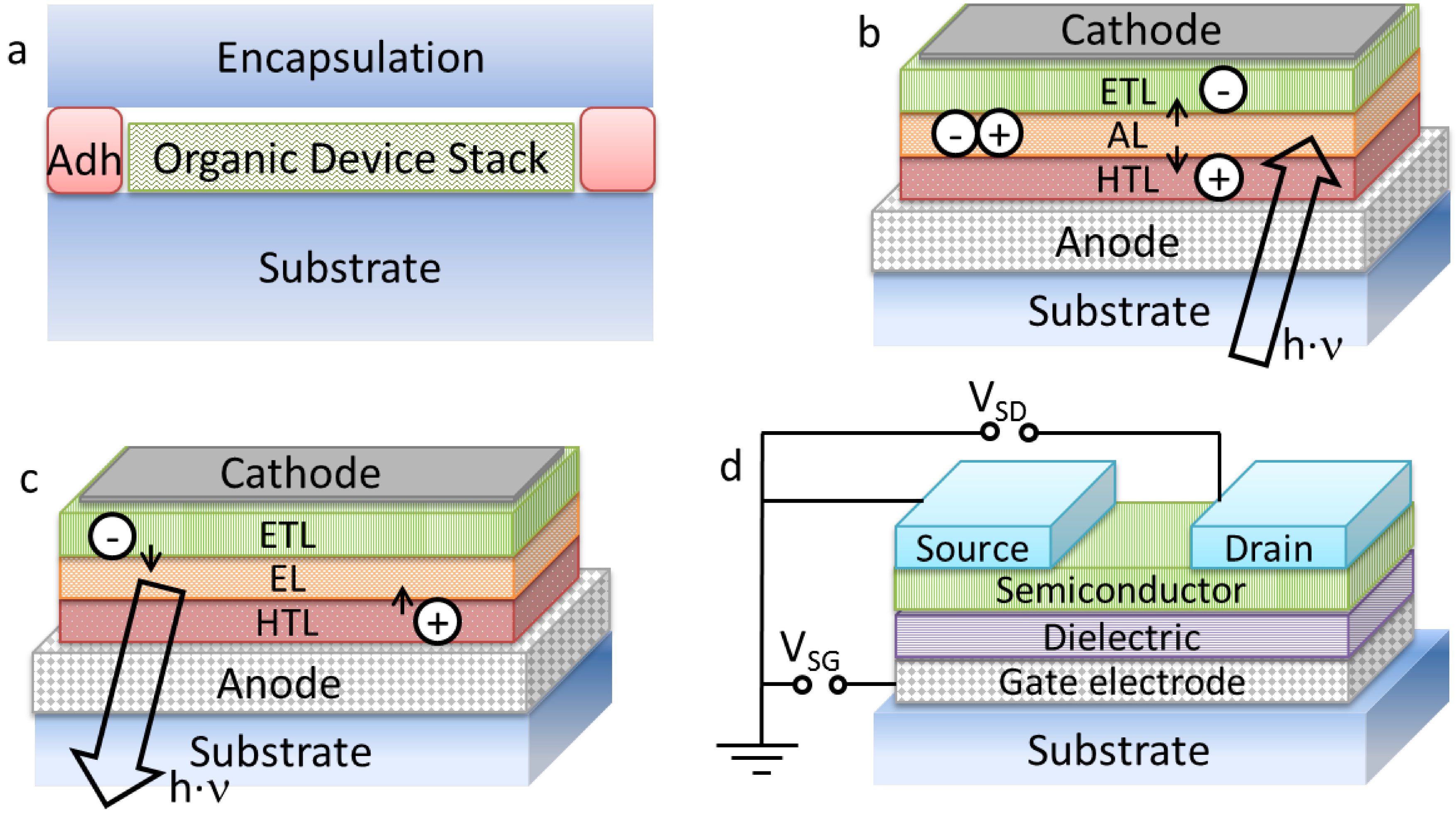
Sustainable development and economics is one of the greatest challenges mankind has to face in the 21st century [5]. We have to rethink the character and design of our technologies, products and how they are produced. This has to result in changes to marketing patterns, distribution, usage and recycling.
The recycling of discarded products could be a way to save materials and energy. However, a basic requirement of recycling is the collection of the used products. Most (mobile) consumer electronics are small and the majority of people will rather throw them into the waste than collecting and bringing them back to collection facilities [6]. This behavior will show a negative impact particularly in countries with inadequate waste regulations. Thus, the development of non-toxic, biodegradable electronics would be a step forward to diminish the problem.
In order to prevent any negative impact of organic chemicals which are supposed to be introduced into the environment, it is necessary and important to duly assess the environmental and toxicological safety of these materials. Typically, the material itself as well as its potentially resistant residues (after biodegradation) has to be characterized [4]. Important test procedures comprise the “water-soluble intermediates-Daphnia test” and the “plant growth test”. The former one is of great importance because water-soluble intermediates may enter the groundwater and are easily absorbed afterwards by other organisms. The test has to be carried out in accordance to DIN 38412 where 10 water fleas are exposed to different concentrations of the designated pollutant at 20 °C and pH 7.0. In addition, a control stock solution is prepared where the testing material degrades enzymatically. After 24 h, the remaining number of swimming water fleas is evaluated. With this relation of concentration and living fleas, the toxicity can be evaluated.
The plant growth test studies the eco-toxicity of materials and is described in EN 13431, annex E. There, the seedling growth behavior of four plant types (wheat, summer barley, mustard, and mung bean) is investigated both with treated and control soil. Subsequently, the harvest yield is correlated with the different soil mixtures. After these tests have been passed successfully, further experimentation involving higher organisms such as earth worm, rabbits, guinea pig and rats will follow.
According to the chemical structure of classic organic semiconductors, the water solubility will be very low for the majority of this material class due to their extended π-system and the lack of highly polar functional groups. At the same time, there are plenty of aromatic compounds, structurally very similar to organic semiconductors, which are classified as toxic. Thus, it is mandatory to carefully investigate the hazardous impact of each designated “biodegradable” compound.

3. Components

Along with organic semiconductors, organic electronics comprise various other components like carrier substrates, electrodes, dielectrics, adhesives, and the organic semiconductor itself. Here, the term “organic” is considered according to the chemical definition, thus being mainly composed of hydrogen and carbon. Depending on their use, organic semiconductors are often sensitive against water and moisture and show an increasing number of defect sites over the operational lifetime. Therefore, the organic layers are protected with an encapsulation material (could be the same as the carrier substrate) and an adhesive as shown in Figure 3. It is often recommended that both the adhesive as well as the encapsulation material have to feature a water vapor transmission rate (WVTR) smaller than 10−5 g/(m2 day) [7]. The controversial requirements of being insensitive against water or oxygen and biodegradable at the same time are very challenging. Thus, for appropriate discussion, each component is described separately.
Figure 3. Schematic illustration of (a) the cross section of an organic device consisting of an organic device stack deposited on a substrate, encapsulated with a barrier material that is fixed with an adhesive (Adh). The composition of the organic device stack defines the properties of an OSC (b), an OLED (c), or an OTFT (d).
Electronics 03 00444 g003
Depending on the device functionality, the organic device stack is composed of a certain material layer sequence which can result in organic light emitting diodes (OLEDs), organic solar cells (OSCs) or organic thin film transistors (OTFTs). Organic device stacks of these three types are represented in Figure 3.
The layer structures of OLEDs and OSCs are very similar. In the common bottom structure where a transparent anode on a transparent substrate is used, the device fabrication may start with deposition of the electrode on the substrate material. A barrier free charge carrier transport from the anode to the hole transport layer (HTL) is ensured by limiting the difference of the highest occupied molecular orbitals (HOMOs) of the single materials to less than 0.3 eV for the interfaces [8]. Similar requirements exist between HTL and the functional layer, i.e., absorption layer (AL) for OSCs and emission layer (EL) for OLEDs. In both cases, it is necessary to prevent the electrons from entering the HTL and, vice versa, the holes from entering the ETL. This can be realized by implementing materials with favorable energy levels providing transport barriers that block either electrons or holes. On the electron transporting side from AL to ETL, the lowest unoccupied molecular orbitals (LUMOs) of the single materials are used and have to align with the work function of the cathode.
The value of the charge carrier mobility of organic semiconductors has to be high for all organic electronic devices; however, achieving a sufficiently high value is even more important when used in OTFTs. Usually, for organic semiconductors, the hole mobility is larger than the electron mobility. Hence, depending on the electrode polarization, holes are accumulated on the semiconductor/dielectric interface after a voltage is applied between gate and source. Due to the voltage between drain and source, the majority of charge carriers are able to move along the interface.

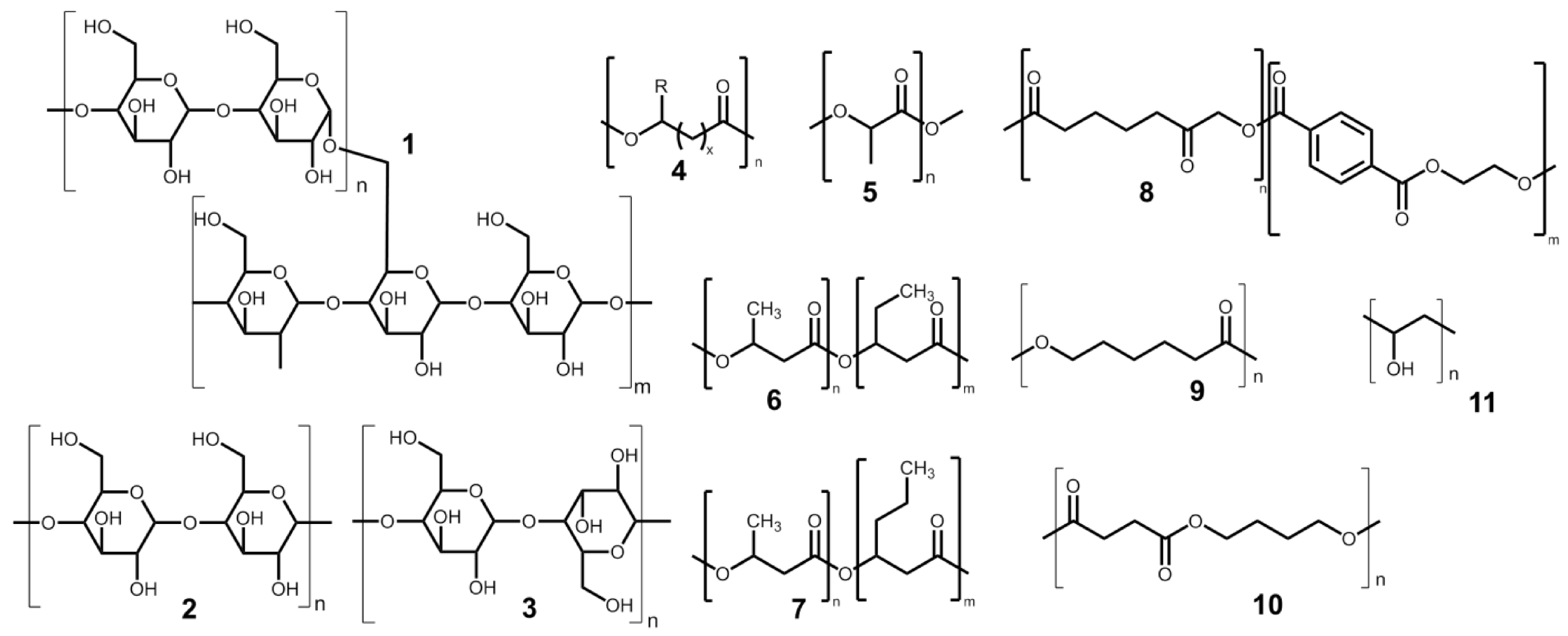
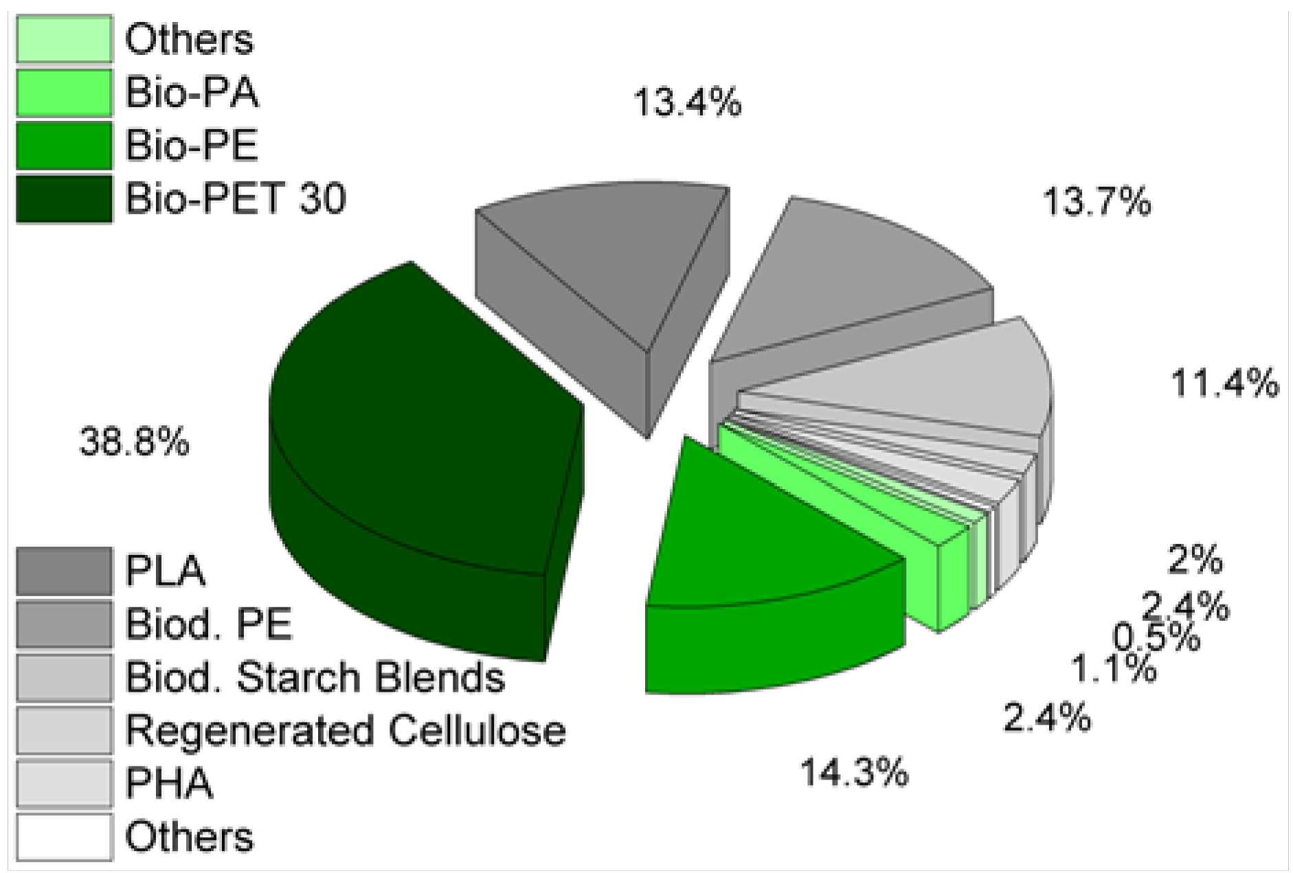
3.1. Substrate Materials

One of the most decisive properties of organic electronics to successfully enter the future market is their inherent flexibility due to the weak intermolecular forces of organic semiconductors. Along with the ductility allowing new application scenarios, also the possibility to use potentially low cost roll-to-roll processes will enable use of the application in consumer electronics. By defining the mechanical properties and providing certain barrier properties, the substrates highly influence the device lifetime. Conventionally, plastic substrates such as polyethylene terephthalate (PET), polyethylene naphthalate (PEN), polycarbonate (PC), and polyimide (PI) have been widely used. However, decomposition for all these polymer foils may take 30–450 years [9], thus causing a serious waste problem in some areas of the world. In addition, their production costs are highly dependent on the oil price.
Therefore, new biodegradable, bio-based, flexible and transparent substrates have attracted considerable attention. Depending on their composition, they may derive from earth-abundant renewable materials or still rely on fossil resources. Figure 4 and Figure 5 schematically illustrate the variety of biodegradable plastics.
Figure 4. Schematic representation of the diversity of degradable materials.
Electronics 03 00444 g004
Figure 5. Established biodegradable polymers potentially usable as carrier substrates. Starch originating from potatoes or corn consist of the branched amylopectin (1) and linear amylose (2). Cellulose (3) is structurally similar, but differs from the bonding type between the glucose monomers. Polyhydroxy alkanoates (PHA) (4) and polylactic acid (PLA) (5) may derive from various sugars, fatty acids or starch. Other typical representatives are polyhydroxybutyrate-co-valerate (PHBV) (6) and polyhydroxybutyrate-co-hexanoate (PHBH) (7). Polybutylene adipate-co-terephthalate (PBAT) (8) is a polymer with aromatic fragments. Polyesters are represented by polycaprolactone (PCL) (9), and polybutylene succinate (PBS) (10). Polyvinyl alcohol (PVA) (11) has a rather simple structure compared to the aforementioned structures.
Electronics 03 00444 g005
For example, starch is transformed into glucose, which is further used as fermentation feedstock for monomers, e.g., lactic acid for poly lactic acid (PLA) or polyhydroxy alkanoates (PHA) production. Other feedstocks for fermentative monomer production are sucrose, glycerol, or plant oil. Intensive work has been carried out to access cellulose raw materials not only for bioethanol production, but also for different chemical intermediates and monomers such as lactic and succinic acid. Whereas the materials 17 are derived from these renewable resources, the compounds 811 originate (partly) from fossil fuels. Aliphatic polyesters (9, 10) are the first completely fossil-based polymers which are biodegradable at the same time. Structures such as polybutylene adipate-co-terephthalate (PBAT) (8) represent a mixture of both natural and synthetic origin. The only existing biodegradable polymer with an all-carbon backbone is polyvinyl alcohol (PVA). The main substrate type that has successfully been integrated in organic electronic technology in recent years is cellulose in its various modifications [10,11,12,13]. Although the initial roughness of these substrate types is initially challenging, the roughness level could be lowered either by adjusted fabrication parameters or by additional (bio)coatings. Another biodegradable and well investigated polymer for substrate use is poly lactic acid [14]. For further detailed information about this material class, the authors recommend the excellent overview about biodegradable polymers given by Breulmann and co-workers [15].

3.2. Adhesives

The development of biodegradable adhesives is a very critical issue for achieving biodegradable electronic products. A biodegradable material which is resistant against water appears to be mutually preclusive (exception e.g., shellac). In the subsequent paragraphs, examples are presented which are mainly dedicated for packaging purposes and thus have less distinctive barrier requirements than devices targeted for long term applications like displays—hence, the impermeability against water is usually not evaluated.
In 1996, a biodegradable, polymerizable adhesive consisting of diacrylate with mono- or disaccharide residues was described [16], while later in 2002 an eco-friendly adhesive based on soy protein was developed [17]. In the latter example, additives such as copper naphthenate, o-phenyl phenol or copper-8-quinolate are inserted to improve the moisture stability. An interesting report shows how a biodegradable gecko-inspired tissue adhesive is developed while being resistant to water treatment for a sufficiently long time [18]. Another work combines human serum albumin and organic acid-based crosslinkers with active ester groups, creating solid-liquid type adhesives without the presence of any organic solvents [19].
A water-based conductive adhesive for electrical interconnects and printed circuits was published by Yang and co-workers [20]. This environmentally harmless, but not biodegradable, adhesive based on polyether diol was stable for 1440 h at 85 °C and a relative humidity of 85% and can potentially be used for flexible consumer electronics.
Bettinger et al. determined biodegradable adhesives for organic electronics and asserted that they should be highly crystalline, highly hydrophobic and easy to process while maintaining performance under high-salinity environments and at elevated temperatures. Poly-L-lactide turned out to be a promising candidate because it can repel water (and vapour) for several months [21].
While these examples show that a variety of biodegradable adhesives are available and easily accessible, information about their barrier properties and potential applications in organic electronics is still missing.

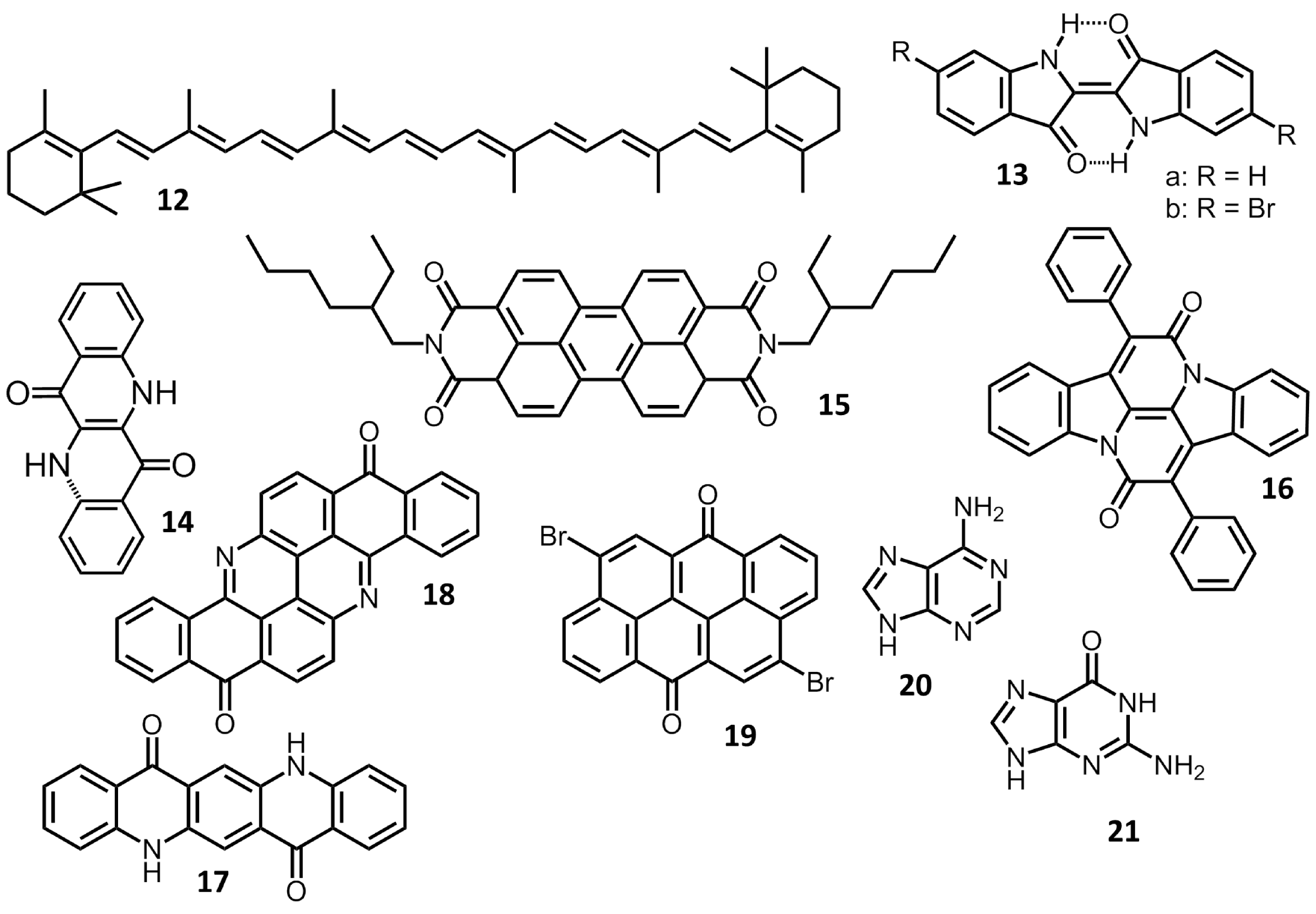
3.3. Organic Semiconductors

A requisite of organic semiconductors is the existence of a π-conjugated carbon backbone allowing the delocalization of electrons. Along with the delocalization of electrons, also the absorptivity of these molecules increases with the extension of the π-conjugation. Thus, a great variety of natural dyes are existing that can also be considered as organic semiconductors. Such material classes comprise polyenes (like the carotenes), quinones, anthraquinones, indole, pyran and oligopyrrol colorants as well as pteridines, isoquinolines and phenoxazine. Most of them comprise several aromatic structures and functional groups such as hydroxyl-, amine-, imine, or even halide groups. Thus, in order to explore the usage of organic compounds that are both semiconducting and biodegradable, scientists were focusing on these natural dye structures and their derivatives. The most commonly used so far are presented in Figure 6.
Figure 6. Chemical structures of biodegradable or biocompatible organic semiconductors (1219) and dielectric materials (20, 21).
Electronics 03 00444 g006
The natural compound melanin has extensively been studied as semiconducting biomaterial. Usually, this compound exhibits low charge carrier mobilities and thus, melanin would not be suitable for electronic devices due to its highly disordered chemical structure [21]. However, evidences have been shown that contradict this hypothesis [22]. Mostert et al. has found that free charge carriers from comproportionation reactions are produced by water absorption. Therefore, melanin is a chemical self-doping polymer and can, in fact, be used for bioelectronics applications.
Furthermore, the focus has turned towards carotenoids as applicable semiconducting materials. The most widely reported examples of these small-molecule polyenes are bixin and β-carotene (12). The suitability of biodegradable materials for their utilization in organic electronics, in particular organic thin film transistors, is explored by Irmia-Vladu and his co-workers [21,23,24,25,26]. The semiconductors are used as gate-controlled charge transport material between the source and drain electrodes [23]. Additionally, natural chlorophyll, hemin, phenazine, terpenoid molecules and indigo (13a) are listed as natural p- and n-type semiconductors, whereas nature inspired materials such as indanthrene yellow G, brilliant orange RF, epindolidione (14), perylene diimide (15) and naphthalene diimide are described as biocompatible. These synthetic organic semiconductors have higher field effect mobilities (4 × 10⁻⁴–1.5 cm2 V−1·s−1) than the natural organic semiconductors (~10−4 cm2 V−1·s−1), are suitable for vacuum processing, highly stable and barely toxic.
In 2011, Głowacki et al. evaluated dyes from the material classes acridones, anthraquinones, carotenoids, and indigoids [27] and also determined the charge carrier mobilities in the range of ~10−4 cm2 V−1·s−1 when applied in OTFTs. Ambipolar indigoids and quindacridones showed the most promising semiconductor properties due to their long-range order, crystallinity and highly dielectric characteristics. For comparison, the electrical properties are given in Table 1.
Table 1. Overview of electrical properties of natural semiconductors comprising the energy levels (HOMO, LUMO), the band gab Eg determined by cyclic voltammetry (CV) or by optical measurements, the charge carrier mobility for holes (µh) and electrons (µe) as well as the dielectric constant εr [27].
MaterialHOMO (eV)LUMO (eV)Eg CV (eV)Eg Optical (eV)µ (cm2/VS)εr
Indigo (13a)−5.5−3.81.71.7µe = 1 × 10⁻², μh = 1 × 10−24.3
Tyrian Purple (13b)−5.8−4.01.81.9µe = 0.3 [28], μh = 0.26.2
Cibalackrot (16)−5.6−3.52.12.0µe = 9.3 × 10⁻³, μh = 5.3 × 10−34.8
Quinacridone (17)−5.4−2.92.52.0μh = 0.15.2
Vat Yellow 1 (18)−6.3−3.62.72.3μe = 4.2 × 10−23.8
Vat Orange 3 (19)−6.2−3.82.42.1µe = 8.8 × 10−33.8
β-carotene (12)−5.84−3.54NA2.3μh = 4 × 10−42.5
Along with great electrical properties, thin films of indigo dyes show strong absorption bands (450–730 nm) and are thus highly interesting for other optoelectrical applications like organic solar cells. The thermal and photochemical stability, the low band gap of 1.7–1.8 eV (as tyrian purple 13b) and high planarity of the molecules are of great advantage for indigo and its derivatives.
While natural organic semiconductors have been evaluated for device fabrication, the classic n-type material fullerene C60 has been investigated with regard to its toxic nature. For this purpose, C60 nanowhiskers have been exposed to macrophage cells and metabolized on average 6 μm long and 660 nm wide (in diameter) C60 nanowhiskers. No toxic effects on mammalian cells have been observed [29]. A good overview about toxicity aspects of C60 is given by Partha and Conyers, in particular regarding the importance of functionalized fullerenes and its dose dependency [30]. Neither in vitro studies on supramolecular structures nor in vivo studies on normal “cell” morphology or viability have revealed any toxicity which is in contradiction to listed references [30]. Hence, the toxicity of C60 remains under debate.
Additionally, it is noteworthy that the indanthrene dyes biodegrade slowly compared to natural compounds [23], however, perylene diimide and epindolidione show little toxicity, thus, they will not be assigned as “biodegradable” [24,25].

3.4. Electrode Materials

Compared to the components described before, the replacement of conventional electrodes appears to be rather challenging since metals can hardly be metabolized.
The degradation of biocompatible porous silicon nanowire barcodes was shown by Chiappini and co-workers in 2010 [31]. When exposing the barcodes to phosphate buffered saline solution at 20 °C, a complete degradation within 24 h is observed, while the exposure to oxygen plasma resulted in oxidation within 72 h. It has been concluded that the surface influences the degradation rate.
The conductivity of the biological conductor melanin highly depends on its hydration level. Proton conductivity is the mechanism which is responsible for the charge transport. It can be used as thin film for biomedical applications. Synthetic conducting polymers such as polyaniline, polypyrrole, and polythiophene can be used as organic electrode as well, but little is known concerning their biodegradability. Only for PEDOT:PSS does data exist suggesting it is not toxic to living tissue [32].
A good overview about degradable, biocompatible metals for medical applications is, in particular, provided by Hendra Hermawan [33]. The main focus has centred on magnesium- and iron-based alloys. For these examples, the metals degrade in a special physiological environment that is comparable to the human body. The degradation behaviour of Mg, Fe, Mn, and Pd alloys is presented and electrical resistivities ranging from 0.044 Ω·mm2/m (Mg) to 0.43 Ω·mm2/m (Mn) have been determined.
A comparable article is published by Cheng et al. [34]. The suitability of Fe, Mn, Mg, Zn, and W for clinical biomedical applications has been tested and cytotoxic properties have been isolated for manganese and zinc.

3.5. Dielectric Materials

The main function of dielectric materials is to prevent electrical current flow which is needed to insulate different electrical connections. The main requirements for their use in OTFTs are low dielectric losses and leakage currents as well as high breakdown strengths [23,24,26].
Apart from shellac [35], natural dielectrics originating from two material classes have been investigated in 2010. The first group comprises sugar-based small molecules such as fructose or lactose which can be wet-processed from water and/or dimethyl sulfoxide. The second group consisted of various nucleobases like adenine, guanine, cytosine and thymine. Their dielectric properties fulfil the requirements for the use in OTFTs. Nucleobases such as adenine (20) and guanine (21) can easily be purified and evaporated as thin films (up to 2.5 nm) which enable DNA-like sequences [23,24,26]. Moreover, DNA which has been functionalized by a cationic surfactant reaction became soluble in polar solvents and allowed wet coated thin films. Thus, it can easily be applied as electron blocking layers (EBLs) in OLEDs or as gate dielectrics in OTFTs [23,24,32]. In addition to these materials, polyvinyl acetate which can be cross linked by UV exposure, has been used as gate dielectric, too [21]. Advanced n-type organic transistors and light emitting transistors have successfully been built up by using natural silk fibroin, whose degradation lifetime may range from weeks to years [36]. The easily obtainable and inexpensive natural compound chicken albumin is utilized as gate dielectric in OFETs, too [37]. The spin-coated and thermally treated, unmodified material generates high quality thin films for devices with excellent performance. Furthermore, organic thin film transistors implemented in complementary inverters have been presented utilizing spin-coated natural cellulose as high k gate dielectric [38]. The inverters have shown good performance including an excellent switching behavior. Finally, Khor and Chung gave a good overview about the use of different natural materials as dielectrics and discussed the structural and electrical behavior of screen printed, commercially purchased aloe vera gel [39]. In particular, the dependence on the drying temperature, duration and thickness of the thin film on glass substrate is studied.

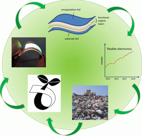
4. Applications and Markets

4.1. Consumer Organic Electronics

In the field of electronics, bio-based materials receive increasing interest because they show potential for having a positive impact on the environment. Already, years ago, IBM investigated bio-based materials like lignin as laminate and demonstrated their potential to save resources [40]. High-tech companies like Samsung and Apple are already using biodegradable components in their electronics as covers for their products such as the Samsung Galaxy S3 or the iPhone 4/4S/5. In addition, a variety of examples have been published where organic electronics have been applied on biodegradable substrates. Zhu and co-workers have used both nanopaper and regenerated cellulose films (RCF) for organic electronics. Both types consist of cellulose nanofibres and differ only in their orientation. As a result of the better scattering properties, an appropriate handling temperature and similar roughness compared to classic PET, green OLEDs have been successfully demonstrated on such substrates [41]. Another work showed that even the deposition of indium tin oxide (ITO) on bacterial cellulose by r.f. sputtering is possible. The resulting OLED device achieved 25% of the reference device performance produced on conventional glass [11]. Although ITO has to be replaced on the long-term time scale, this report shows that common thin film technology can also be applied on biodegradable substrate types with slight adaption of the processing parameters.
Another promising work with bacterial cellulose as carrier substrate demonstrated the proof of concept of developing a dynamic display by using simple electric dopants and inks [12]. With regard to energy storage devices, the conductivity of conventional paper has been increased by depositing carbon nanotubes and silver nanowires [42], whereas cellulose fibers have also been used to improve the mechanical properties of electronically conductive polymers while retaining very high conductivities [43]. Large-area organic electronics on unmodified paper have been fabricated by Barr and co-workers. They have built monolithically integrated OSC on paper with a dimension of 7 × 7 cm2 [44]. Although the subcells made on paper achieved lower efficiencies than those fabricated on glass, still a total voltage of 49 V has been realized (compared to 70 V for the sample on glass). The complete decomposition in water has also been shown for OSC on cellulose nanocrystal substrates, which have achieved efficiency values of 2.7%. However, effects originating from the metal electrodes or the conventional organic semiconductors have not been addressed [9].
In the field of field effect transistors (FETs), flexible devices have been fabricated with cellulose paper as dielectric material and achieved results comparable to conventional PET or glass substrates. Even the application of OTFT on conventional bank notes has been impressively demonstrated [44,45]. With regard to the semiconductor material itself, anthraquinones, perylene bisimides and indigo are applicable as semiconductors in fully “green” OTFTs [16,35].
According to market prediction, the production of biodegradable plastic will increase fivefold from 1102 tons (2010) to 5779 tons by 2016 [3]. On the one hand, a greater availability of biodegradable plastic will increase the research interest in that field resulting in better device performance; on the other hand, the consumer will most likely request more and more green technology. However, it is unlikely that biodegradable organic electronics will enter the market of entertainment electronics where long-term stability is a necessary requirement. The characteristic of biodegradability will be accompanied by short lifetimes due to sensitivity against water and oxygen. However, in the field of smart packaging, this is an advantage due to its intention for single use and fast insertion into the recycling system. At present, the demand for smart packages with sensing and information technology is already continuously rising, though it is very expensive due to used resources.

4.2. Medicine

The need for a healing support is often temporary in the field of medicine [33]. The application of fully biodegradable materials will allow a complete degradation after fulfilling its function which is much better than an additional surgery. Therefore, the use of biodegradable electronics for medical applications like biomedical implant devices for energy harvesting, medical diagnosis, sensing, photonic biomedical devices, tissue engineering scaffolds or drug delivery is highly anticipated [18,19,23,26,31,32,35,46,47,48,49,50,51]. Benefits for biomedical science, including biocompatible devices, are predicted because of their ability to align to curved, elastic, and soft surfaces. Biocompatibility is defined as a sustainable, mutual co-existence of biomaterials and tissues [52]. A comprehensive overview about bio-integrated electronics for medical applications over the last 10 years is given by Koo and co-workers [53].
Biocompatible/biodegradable microelectromechanical systems (MEMS) received growing interest, in particular for biomimetics, tissue engineering and drug delivery [54]. The biodegradable MEMS are fabricated by micromolded polycaprolactone with milimetersized reservoirs, which are filled with water and covered with a gold membrane.
King et al. have explored biodegradable polymers for therapeutic medicine [55]. Three dimensional monolithic microdevices are bonded from stacked, microstructured PDMS mold. The resulting microfluidic networks show improved speed, resolution and precision as well as reproducibility, manufacturability and scalability compared to previous methods. A bacterial cellulose membrane is used as flexible substrate for OLEDs for potential photodynamic therapy to treat skin cancer and other skin diseases [11].
Additionally, it has been shown that a combination of organic semiconductors and bioactive molecules have great potential for clinical applications, especially for bioresorbable temporary medical implants [21]. Muskovich and Bettinger focused on the translation of bioelectric communication between the intra- and inter-cellular environment as well as the important role of material selection and the subsequent quality of the biotic–abiotic interfaces [56].

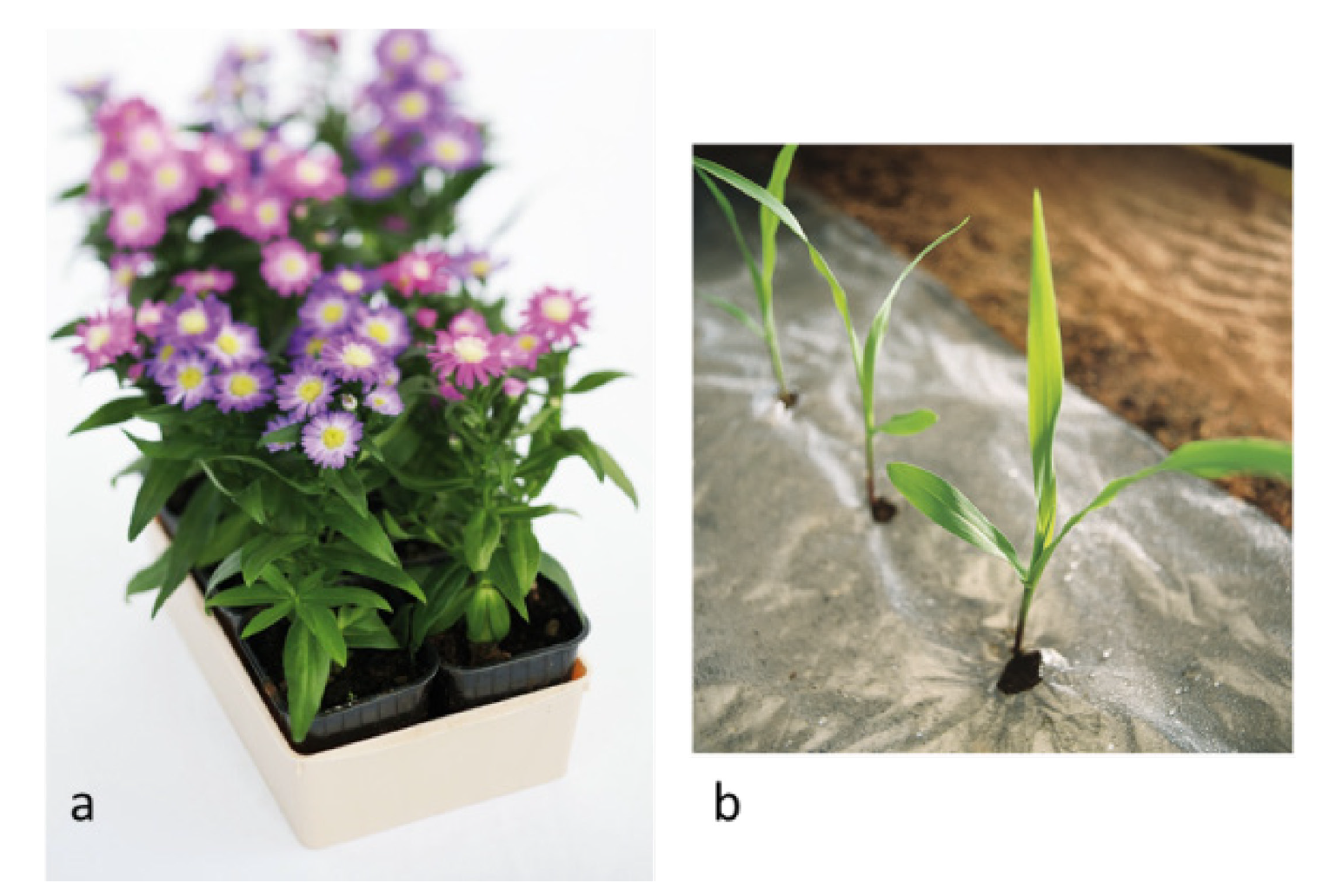
4.3. Agriculture/Horticulture

In the field of agriculture and horticulture, bio-plastics are already widely used in the form of foils, ribbons and planting pots as displayed in Figure 7. Reasons for their use are the adjustable lifetime and the advantages of fully compostable materials [57]. In order to study the impact of these materials on soil, degradation dynamics of agricultural films have been examined in more detail by IR thermography, SEM analysis and mechanical tensile tests [58]. Further application scenarios for food safety have been discussed such as pesticide and microorganism detection [59].
To the best of the authors’ knowledge, there are no publications about the use of biodegradable electronics in horticulture or agriculture. One reason could be that electronics have been generally uncommon in this field. However, the possibility of integrating electronics without negative impact on the environment can open new opportunities. One approach could comprise sensors for nutrients or water in soil that change their shape (hydrogels in polymer micro systems) or color (OLED). Further, the installation of a sensor directly at the plant to measure special surface behavior due to external influences is conceivable.
Figure 7. Examples of biodegradable materials: (a) plant pot (©Limagrain) and (b) mulching film (©BASF).
Electronics 03 00444 g007

5. Conclusions

We have shown the recent progress and great potential of bio-organic electronics for the future consumer market, medical field and agriculture. A survey performed by Theinsthid and co-workers showed that businesses are highly interested in “greener” electronics because they expect economic advantages over their competitors and growth opportunities for their companies, as well as to more easily satisfy customer requirements and receive new opportunities in new markets [60].
These business interests are accompanied by distinctive market growth of cheap, flexible organic electronics which is expected to continuously increase, reaching a market share of approximately 12 billion USD by 2020 [61]. These cheap electronics are supposed to enter the huge market of smart packaging that appears to be the most promising field for biodegradable organic electronics. In addition, it is not too easy to estimate the market benefits of these bio-based electronics for disease detection or clinic therapy which need to be bio-compatible. These requirements will be more easily achieved if the materials are biodegradable or of bio-based origin.
However, it should be mentioned that there are obstacles before this kind of technology will fulfill the promise of sustainability and wealth. Although tremendous progress has been made to develop biodegradable materials, which completely degrade at the domestic compost heap, often the so-called biodegradable materials used today are still not fully converted in industrial composting plants and significantly disturb the sensitive waste management system. This has led to recommendations from various waste disposal associations to exclude biodegradable plastics from the regular compost bin. In addition, it will remain a matter of discussion if there is a real need for biodegradable electronics when the waste recovery system of a country is effectively working, and then to foster the disposable culture among the citizens further. However, the usage of bio-based materials would bring a different societal value by promoting the development of plastics which originate from regrowing resources ensuring their wide use also after the petroleum age.
Furthermore, scientific proofs about the designated positive ecologic impact of bio-materials are still missing. Examples have been reported, where no evidence is seen for any environmental advantage, by substituting established materials with bio-based and biodegradable ones [32]. Profound life cycle analysis according to DIN EN ISO 14040 and 14044 are strongly requested by the experts to show that the utilization of bio-based and/or biodegradable materials will reduce CO2-emission as well as the consumption of scarce resources and that the development of biodegradable products will have only positive long-term effects.

Author Contributions

Both authors equally wrote the manuscript, outlined the figures, contributed to discussion and finalized the manuscript.

Conflicts of Interest

The authors declare no conflict of interest.

References

  1. Seymour, R.B.; Deanin, R.D. History of Polymer Composites, 1st ed.; VNU Science Press BV: Utrecht, The Netherlands, 1987. [Google Scholar]
  2. Singh, B.; Sharma, N. Mechanistic implications of plastic degradations. Polym. Degrad. Stab. 2008, 93, 561–584. [Google Scholar] [CrossRef]
  3. BIOPLASTICS—facts and figures. Available online: http://en.european-bioplastics.org/wp-content/uploads/2013/publications/EuBP_FactsFigures_bioplastics_2013.pdf, last (access on 4 March 2014).
  4. Shah, A.A.; Hasan, F.; Hameed, A.; Ahmed, S. Biological degradation of plastics: A comprehensive review. Biotechnol. Adv. 2008, 26, 246–265. [Google Scholar] [CrossRef]
  5. Rifkin, J. The Third Industrial Revolution: How lateral Power is Transforming Energy, the Economy, and the World, 1st ed.; Palgrave Macmillan: New York, NY, USA, 2011; pp. 1–32. [Google Scholar]
  6. Griese, H.; Stobbe, L.; Middendorf, A.; Reichl, H. Environmental compatibility of electronics—A key towards local and global sustainable development. In Proceedings of the 2004 International IEEE Conference on the Asian Green Electronics AGEC, Hong Kong, China, 5–6 January 2004; pp. 158–163.
  7. Fahlteich, J.; Amberg-Schwab, S.; Weber, U.; Noller, K.; Miesbauer, O.; Boeffel, C.; Schiller, N. 29.1: Ultra-high barriers for encapsulation of flexible displays and lighting devices. SID 2013, 44, 354–357. [Google Scholar] [CrossRef]
  8. Tress, T.; Leo, K.; Riede, M. Influence of hole-transport layers and donor materials on open-circuit voltage and shape of I–V curves of organic solar cells. Adv. Funct. Mater. 2011, 21, 2140–2149. [Google Scholar] [CrossRef]
  9. Zhou, Y.; Fuentes-Hernandez, C.; Khan, T.M.; Liu, J.-C.; Hsu, J.; Shim, J.W.; Dindar, A.; Youngblood, J.P.; Moon, R.J.; Kippelen, B. Recyclable organic solar cells on cellulose nanocrystal substrates. Sci. Rep. 2013, 3, 1–5. [Google Scholar]
  10. Martins, R.F.P.; Ahnood, A.; Correia, N.; Pereira, L.M.N.P.; Barros, R.; Barquinha, P.M.C.B.; Costa, R; Ferreira, I.M.M.; Nathan, A.; Fortunato, E.E.M.C. Recyclable, flexible, low-power oxide electronics. Adv. Funct. Mater. 2013, 23, 2153–2161. [Google Scholar] [CrossRef]
  11. Legnani, C.; Vilani, C.; Calil, V.L.; Barud, H.S.; Quirino, W.G.; Achete, C.A.; Ribeiro, J.L.; Cremona, M. Bacterial cellulose membrane as flexible substrate for organic light emitting devices. Thin Solid Films 2008, 517, 1016–1020. [Google Scholar] [CrossRef]
  12. Shah, J.; Brown, R.M., Jr. Towards electronic paper displays made from microbial cellulose. Appl. Microbiol. Biotechnol. 2005, 66, 352–355. [Google Scholar] [CrossRef]
  13. Kim, D.Y.; Steckl, A.J. Electrowetting on paper for electronic paper display. ACS Appl. Mater. Interfaces 2010, 2, 3318–3323. [Google Scholar] [CrossRef]
  14. Fukuhira, Y.; Kitazonoa, E.; Hayashia, T.; Kanekoa, H.; Tanakab, M.; Shimomurac, M.; Sumi, Y. Biodegradable honeycomb-patterned film composed of poly(lactic acid) and dioleoylphosphatidylethanolamine. Biomaterials 2006, 27, 1797–1802. [Google Scholar] [CrossRef]
  15. Breulmann, M.; Künkel, A.; Philipp, S.; Reimer, V.; Siegenthaler, K.O.; Skupin, G.; Ymamoto, M. Polymers, Biodegradable. In Ullmann’s Encyclopedia of Industrial Chemistry; Wiley-VCH: Weinheim, Germany, 2009. [Google Scholar]
  16. Oosterhoff, R.H. Biodegradable Diacrylates and Adhesives Based Thereon. U.S. 005580940A, 3 December 1996. [Google Scholar]
  17. Kumar, R.; Choudhary, V.; Mishra, S.; Varma, I.K.; Mattiason, B. Adhesives and plastics based on soy protein products. Ind. Crop. Prod. 2002, 16, 155–172. [Google Scholar]
  18. Mahdavi, A.; Ferreira, L.; Sundback, C.; Nichol, J.W.; Chan, E.P.; Carter, D.J.D.; Bettinger, C.J.; Patanavanich, S.; Chignozha, L.; Ben-Joseph, E.; et al. A biodegradable and biocompatible gecko-inspired tissue adhesive. Proc. Natl. Acad. Sci. USA 2008, 105, 2307–2312. [Google Scholar] [CrossRef]
  19. Taguchi, T.; Saito, H.; Iwasashi, M.; Sakane, M.; Ochiai, N. Biodegradable adhesives composed of human serum albumin and organic acid-based crosslinkers with active ester groups. J. Bioact. Compat. Pol. 2009, 24, 546–559. [Google Scholar] [CrossRef]
  20. Yang, C.; Lin, W.; Li, Z.; Zhang, R.; Wen, H.; Gao, B.; Chen, G.; Gao, P.; Yuen, M.M.F.; Wong, C.P. Water-based isotropically conductive adhesives: Towards green and low-cost flexible electronics. Adv. Funct. Mater. 2011, 21, 4582–4588. [Google Scholar] [CrossRef]
  21. Bettinger, C.J.; Bao, Z. Biomaterials-based organic electronic devices. Polym. Int. 2010, 59, 563–567. [Google Scholar]
  22. Mostert, A.B.; Powell, B.J.; Pratt, F.L.; Hanson, G.R.; Sarna, T.; Gentle, I.R.; Meredith, P. Role of semiconductivity and ion transport in the electrical conduction of melanin. Proc. Natl. Acad. Sci. USA 2012, 109, 8943–8947. [Google Scholar] [Green Version]
  23. Irimia-Vladu, M.; Troshin, P.A.; Reisinger, M.; Shmygleva, L.; Kanbur, Y; Schwabegger, G.; Bodea, M.; Schwödiauer, R.; Mumyatov, A.; Fergus, J.W.; et al. Biocompatible and biodegradable materials for organic field-effect transistors. Adv. Funct. Mater. 2010, 20, 4069–4076. [Google Scholar] [CrossRef]
  24. Irimia-Vladu, M.; Sariciftcib, N.S.; Bauer, S. Exotic materials for bio-organic electronics. J. Mater. Chem. 2011, 21, 1350–1361. [Google Scholar] [CrossRef]
  25. Głowacki, E.D.; Irimia-Vladu, M.; Kaltenbrunner, M.; Gąsiorowski, J.; White, M.S.; Monkowius, U.; Romanazzi, G.; Suranna, G.P.; Mastrorilli, P.; Sekitani, T.; et al. Hydrogen-bonded semiconducting pigments for air-stable field-effect transistors. Adv. Mater. 2013, 25, 1563–1569. [Google Scholar] [CrossRef]
  26. Irimia-Vladu, M.; Troshin, P.A.; Reisinger, M.; Schwabegger, G.; Ullah, M.; Schwoediauer, R.; Mumyatov, A.; Bodea, M.; Fergus, J.W.; Razumov, V.F.; et al. Environmentally sustainable organic field effect transistors. Org. Electron. 2010, 11, 1974–1990. [Google Scholar] [CrossRef]
  27. Głowacki, E.D.; Leonat, L.; Voss, G.; Bodea, M.; Bozkurt, Z.; Irimia-Vladu, M.; Bauer, S.; Sariciftci, N.S. Natural and nature-inspired semiconductors for organic electronics. Proc. SPIE 2011, 8118, 81180M:1–81180M:10. [Google Scholar]
  28. Kanbur, Y.; Irimia-Vladu, M.; Głowacki, E.D.; Voss, G.; Baumgartner, M.; Schwabegger, G.; Leonat, L.; Ullah, M.; Sarica, H.; Erten-Ela, S.; et al. Vacuum-processed polyethylene as a dielectric for low operating voltage organic field effect transistors. Org. Electron. 2012, 13, 919–924. [Google Scholar] [CrossRef]
  29. Nudejima, S.-I.; Miyazawa, K.I.; Okuda-Shimazaki, J.; Taniguchi, A. Biodegradation of C60 fullerene nanowhiskers by macrophage-like cells. Adv. Biomed. Res. 2010, 89–94. [Google Scholar]
  30. Partha, R.; Conyers, J.L. Biomedical applications of functionalized fullerene-based nanomaterials. Int. J. Nanomed. 2009, 4, 261–275. [Google Scholar] [CrossRef]
  31. Chiappini, C.; Liu, X.; Fakhoury, J.R.; Ferrari, M. Biodegradable porous silicon barcode nanowires with defined geometry. Adv. Funct. Mater. 2010, 20, 2231–2239. [Google Scholar] [CrossRef]
  32. Irimia-Vladua, M.; Głowackib, E.D.; Vossb, G.; Bauera, S.; Sariciftci, N.S. Green and biodegradable electronics. Mater. Today 2012, 15, 7–8. [Google Scholar]
  33. Hermawan, H. Biodegradable Metals: From Concept to Application; Springer: Heidelberg, Germany, 2012; pp. 13–22. [Google Scholar]
  34. Cheng, J.; Liu, B.; Wu, Y.H.; Zheng, Y.F. Comparative in vitro study on pure metals (Fe, Mn, Mg, Zn and W) as biodegradable metals. J. Mater. Sci. Technol. 2013, 29, 619–627. [Google Scholar] [CrossRef]
  35. Irimia-Vladu, M.; Głowacki, E.D.; Schwabegger, G.; Leonat, L.; Akpinar, H.Z.; Sitter, H.; Bauer, S.; Sariciftci, N.S. Natural resin shellac as a substrate and a dielectric layer for organic field-effect transistors. Green Chem. 2013, 15, 1473–1476. [Google Scholar] [CrossRef]
  36. Capelli, R.; Amsden, J.J.; Generali, G.; Toffanin, S.; Benfenati, V.; Muccini, M.; Kaplan, D.L.; Omenetto, F.G.; Zamboni, R. Integration of silk protein in organic and light-emitting transistors. Org. Electron. 2011, 12, 1146–1151. [Google Scholar] [CrossRef]
  37. Chang, J.-W.; Wang, C.-G.; Huang, C.-Y.; Tsai, T.-D.; Guo, T.-F.; Wen, T.-C. Chicken albumen dielectrics in organic field-effect transistors. Adv. Mater. 2011, 23, 4077–4081. [Google Scholar] [CrossRef]
  38. Petritz, A.; Wolfberger, A.; Fian, A.; Irimia-Vladu, M.; Haase, A.; Gold, H.; Rothländer, T.; Griesser, T.; Stadlober, B. Cellulose as biodegradable high-k dielectric layer in organic complementary inverters. Appl. Phys. Lett. 2013, 103, 153303:1–153303:5. [Google Scholar]
  39. Khor, L.Q.; Cheong, K.Y. Aloe vera gel as natural organic dielectric in electronic application. J. Mater. Sci.: Mater. Electron. 2013, 24, 2646–2652. [Google Scholar] [CrossRef]
  40. Kosbar, L.L.; Gelorme, J.D.; Japp, R.M.; Fotorny, W.T. Introducing biobased materials into the electronics industry—Developing a Lignin-based resin for printed wiring boards. J. Ind. Ecol. 2001, 4, 93–105. [Google Scholar]
  41. Zhu, H.; Xiao, Z.; Liu, D.; Li, Y.; Weadock, N.J.; Fang, Z.; Huang, J.; Hu, L. Biodegradable transparent substrates for flexible organic-light-emitting diodes. Energy Environ. Sci. 2013, 6, 2105–2111. [Google Scholar] [CrossRef]
  42. Hu, L.; Choi, J.W.; Yang, Y.; Jeong, S.; la Mantia, F.; Cui, L.-F.; Cui, Y. Highly conductive paper for energy-storage devices. Proc. Natl. Acad. Sci. USA 2009, 106, 21490–21494. [Google Scholar] [CrossRef]
  43. Nyholm, L.; Nyström, G.; Mihranyan, A.; Strømme, M. Toward flexible polymer and paper-based energy storage devices. Adv. Mater. 2011, 23, 3751–3769. [Google Scholar]
  44. Barr, M.C.; Rowehl, J.A.; Lunt, R.R.; Xu, J.; Wang, A.; Boyce, C.M.; Im, S.G.; Bulovic, V.; Gleason, K.K. Direct monolithic integration of organic photovoltaic circuits on unmodified paper. Adv. Mater. 2011, 23, 3500–3505. [Google Scholar] [CrossRef]
  45. Zschieschang, U.; Yamamoto, T.; Takimiya, K.; Kuwabara, H.; Ikeda, M.; Sekitani, T.; Someya, T.; Klauk, H. Organic electronics on banknotes. Adv. Mater. 2011, 23, 654–658. [Google Scholar] [CrossRef]
  46. Irimia-Vladu, M.; Głowacki, E.D.; Troshin, P.A.; Schwabegger, G.; Leonat, L.; Susarova, D.K.; Krystal, O.; Ullah, M.; Kanbur, Y.; Bodea, M.A.; et al. Indigo—A natural pigment for high performance ambipolar organic field effect transistors and circuits. Adv. Mater. 2012, 24, 375–380. [Google Scholar] [CrossRef]
  47. Kim, D.-H.; Kim, Y.-S.; Amsden, J.; Panilaitis, B.; Kaplan, D.L.; Omenetto, F.G.; Zakin, M.R.; Rogers, J.A. Silicon electronics on silk as a path to bioresorbable, implantable devices. Appl. Phys. Lett. 2009, 95, 133701:1–133701:3. [Google Scholar]
  48. Barhoumi, H.; Maaref, A.; Rammah, M.; Martelet, C.; Jaffrezic-Renault, N.; Mousty, C.; Cosnier, S.; Perez, E.; Rico-Lattes, I. Insulator semiconductor structures coated with biodegradable latexes as encapsulation matrix for urease. Biosens. Bioelectron. 2005, 20, 2318–2323. [Google Scholar] [CrossRef]
  49. Canham, L. Interview—Nanosilicon for nanomedicine: A step towards biodegradable electronic implants? Nanomedicine 2013, 8, 1573–1576. [Google Scholar] [CrossRef]
  50. Lendlein, A.; Sisson, A. Handbook of Biodegradable Polymers: Isolation, Synthesis, Characterization and Applications; Wiley-VCH Verlag GmbH Co. KGaA: Weinheim, Germany, 2013; pp. 309–378. [Google Scholar]
  51. Bazaka, K.; Jacob, M.V. Implantable Devices: Issues and Challenges. Electronics 2013, 2, 1–34. [Google Scholar] [CrossRef]
  52. Williams, D.F. On the mechanisms of biocompatibility. Biomaterials 2008, 29, 2941–2953. [Google Scholar] [CrossRef]
  53. Koo, J.H.; Seo, J.; Lee, T. Nanomaterials on flexible substrates to explore innovative functions: From energy harvesting to bio-integrated electronics. Thin Solid Films 2012, 524, 1–19. [Google Scholar] [CrossRef]
  54. Richards-Grayson, A.C.; Scheidt-Shawgo, R.; Li, Y.; Cima, M.J. Electronic MEMS for triggered delivery. Adv. Drug Deliver. Rev. 2004, 56, 173–184. [Google Scholar] [CrossRef]
  55. King, K.R.; Wang, C.C.J.; Kaazempur-Mofrad, M.R.; Vacanti, J.P.; Borenstein, J.T. Biodegradable microfluidics. Adv. Mater. 2004, 16, 2007–2012. [Google Scholar] [CrossRef]
  56. Muskovich, M.; Bettinger, C.L. Biomaterials-based electronics: Polymers and interfaces for biology and medicine. Adv. Healthcare Mater. 2012, 1, 248–266. [Google Scholar] [CrossRef]
  57. Scarascia-Mugnozza, G.; Schettini, E.; Vox, G.; Malinconico, M.; Immirzi, B.; Pagliara, S. Mechanical properties decay and morphological behaviour of biodegradable films for agricultural mulching in real scale experiment. Polym. Degrad. Stab. 2006, 91, 2801–2808. [Google Scholar] [CrossRef]
  58. Mormile, P.; Petti, L.; Rippa, M.; Immirzi, B.; Malinconico, M.; Santagata, G. Monitoring of the degradation dynamics of agricultural films by IR thermography. Polym. Degrad. Stab. 2007, 92, 777–784. [Google Scholar] [CrossRef]
  59. Sozer, N.; Kokini, J.L. Nanotechnology and its applications in the food sector. Trends Biotechnol. 2008, 27, 82–89. [Google Scholar] [CrossRef]
  60. Theinsthid, P.; Chandrachai, A.; Suwannathep, S.; Keeratipibul, S. Bio-based products: Factors that influence their adoption. In Proceeding of the 2010 IEEE International Conference on Management of Innovation and Technology (ICMIT), Singapore, Singapore, 2–5 June 2010; pp. 354–359.
  61. Das, R.; Harrop, P. Printed, Organic & Flexible Electronics Forecasts, Players & Opportunities 2012–2022; IDTechEx: Cambridge, UK, 2012; pp. 1–58. [Google Scholar]

