4.1. LNA Topology
Reducing the form factor to propose small chip area RFIC designs is essential. To address this purpose, inductor based circuits are now replaced by inductorless RF blocks. Among the tough challenge in the design of inductorless ULP LNA design, is the synthesis of a wideband input matching.
There are two possibilities to achieve a 50 Ω-input impedance inductorless LNA designs. First, a Common Source with resistive feedback technique [
17] could be used but this topology degrades the output impedance and requires a large power for sufficient voltage gain. The other solution is to design a Common Gate topology. This configuration offers the possibility of an easy input matching through the transconductance (gm) of the input transistor. For these reasons, a Common Gate architecture is selected in this work. In order to guarantee a large voltage gain, a gm-boost is added to the common gate architecture [
18].
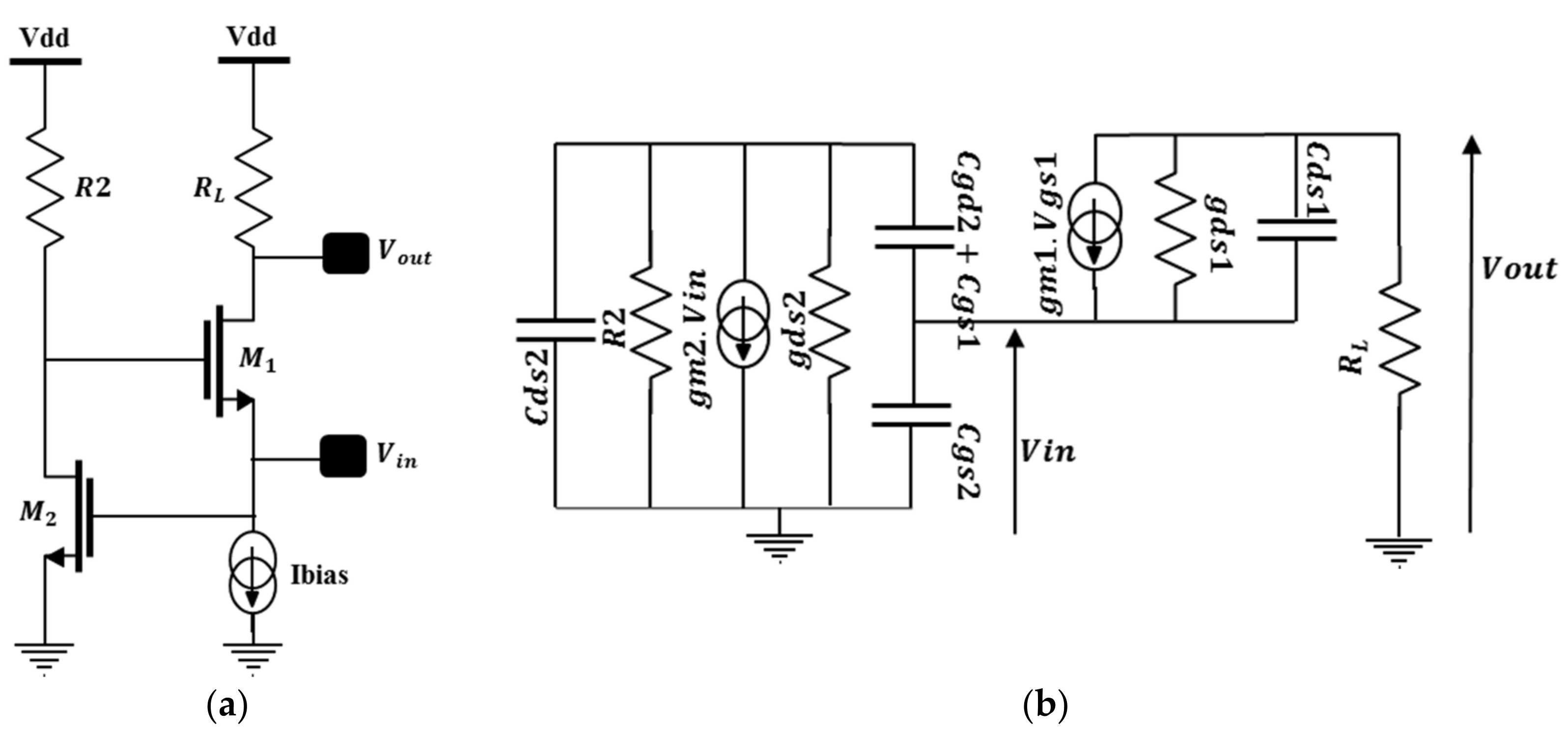
The topology of the proposed LNA and its simplified small signal model are depicted in
Figure 12a,b, respectively. M1 and RL feature the common gate amplifier which is enhanced by the additional common source gm-boost M2-R2. The RF signal is simultaneously applied to the source and the gate of M1 through (M2-R2). This configuration enables an increase of its gate to source voltage (Vgs) and thus enhances the available gain. This architecture offers the possibility to reach large gain, good input matching and reasonable noise figure under low power constraints.
To improve the performance with this topology, which has been already studied in the literature [
12,
19], an exploration of the back gate biasing to further reduce the voltage supply and the power consumption is proposed.
The equivalent voltage gain Gv
LNA, the input impedance Zin
LNA and the Noise Figure NF
LNA of this architecture are given in Equations (3)–(5) respectively.
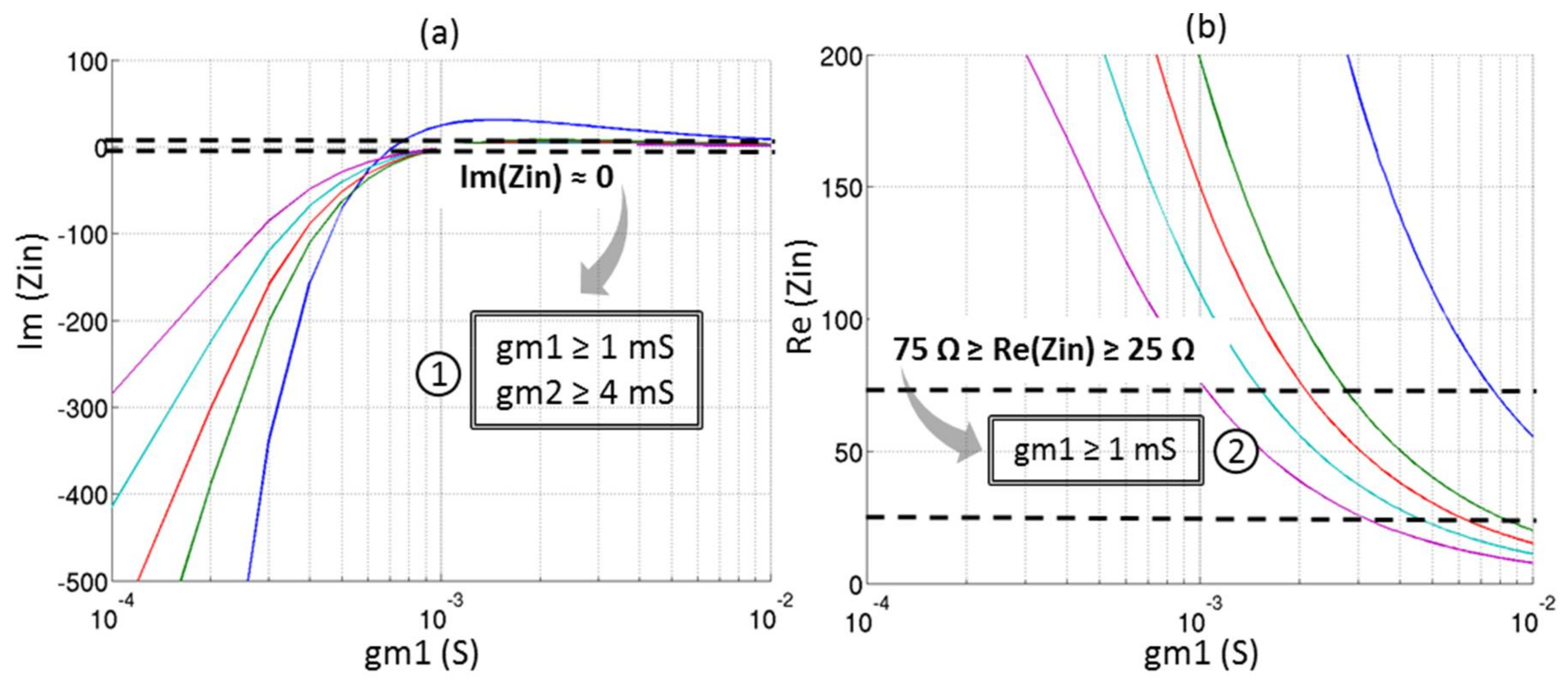
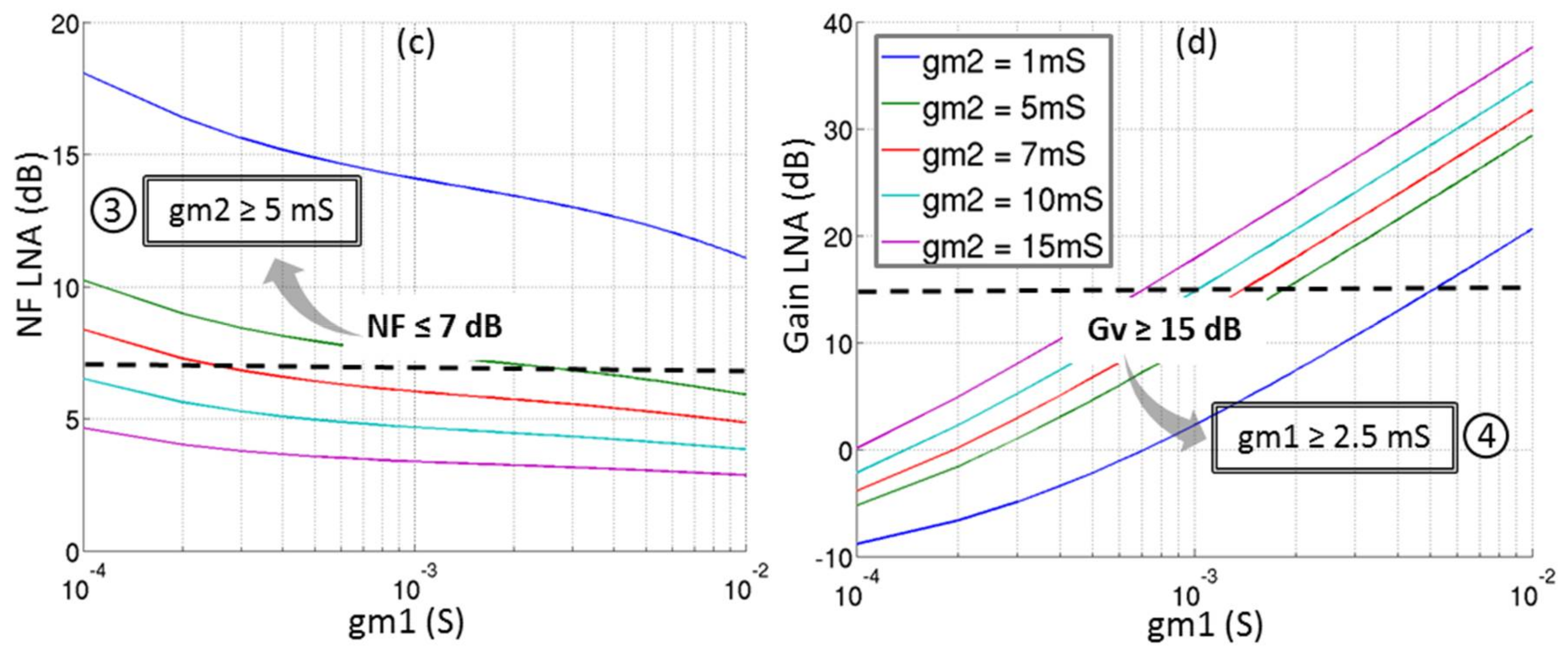
The behavior of the input impedance, the noise figure and the voltage gain described in Equations (3)–(5) are depicted in
Figure 13 for different couples of (g
m1, g
m2). The input matching is considered as acceptable—i.e., real part of Zin between 25 Ω and 75 Ω and imaginary part of Zin close to 0 which gives a S11 under −10 dB. The conditions on (g
m1, g
m2) which fit the requirements of
Table 3 in terms of noise figure (≥7 dB) and voltage gain (≥15 dB) are also illustrated.
In order to optimize the power consumption, the minimum of gm1 and gm2 respecting the conditions ①, ②, ③, and ④ are determined:
- -
gm1 = 2.5 mS;
- -
gm2 = 5 mS.
Therefore, the widths of the transistors have been chosen along with the DC biasing in order to obtain the needed (gm1, gm2) for the minimum power consumption. Active transistors of the LNA (M1 and M2) have minimum gate length to achieve a maximum bandwidth at a minimum power consumption.
The following part proposes a succinct description of the FD-SOI transistor and the body biasing effects in order to evaluate the benefits on the proposed ULP LNA.
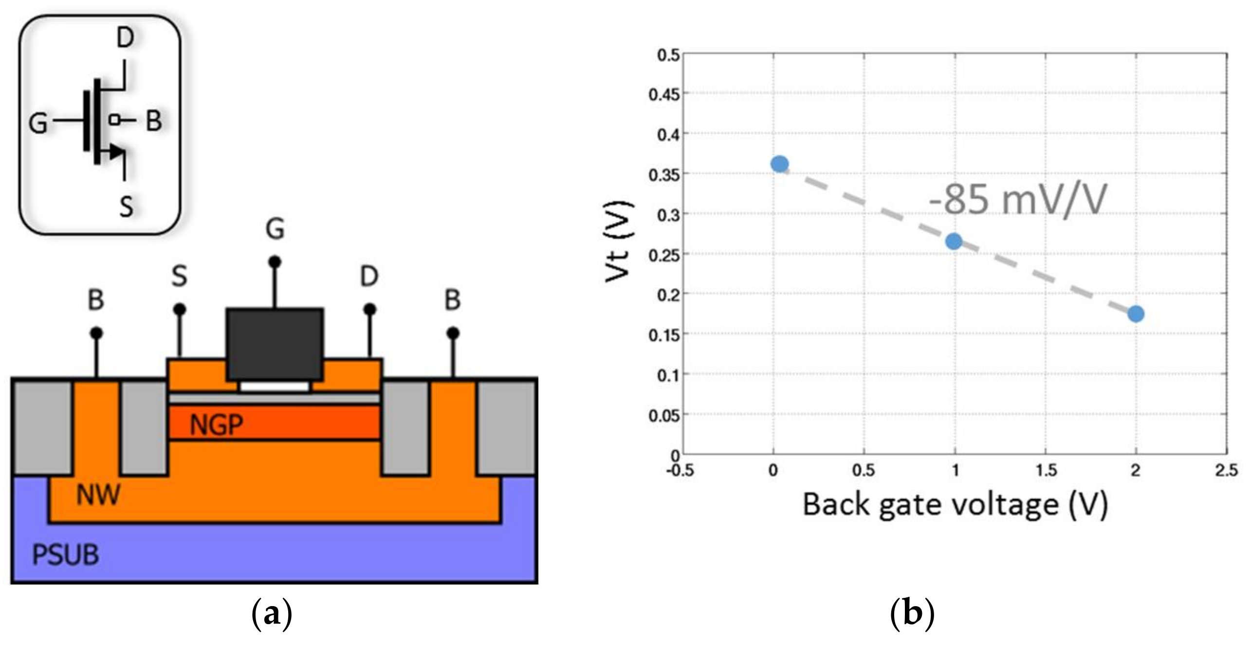
4.2. Body Biasing
Figure 14 illustrates the cross section of an nLVT FD-SOI transistors. As depicted, its channel is isolated from the substrate. Therefore, there is no junction diodes as bulk-drain and bulk-source and body biasing is thus possible. This body biasing enables a reduction of its threshold voltage with a slope of −85 mV/V (see
Figure 14b).
The large variation range on the threshold voltage of the transistor enables new DC operating points on the LNA. In fact, to maintain the saturation of the transistors, the following conditions on the transistor operating point have to be respected:
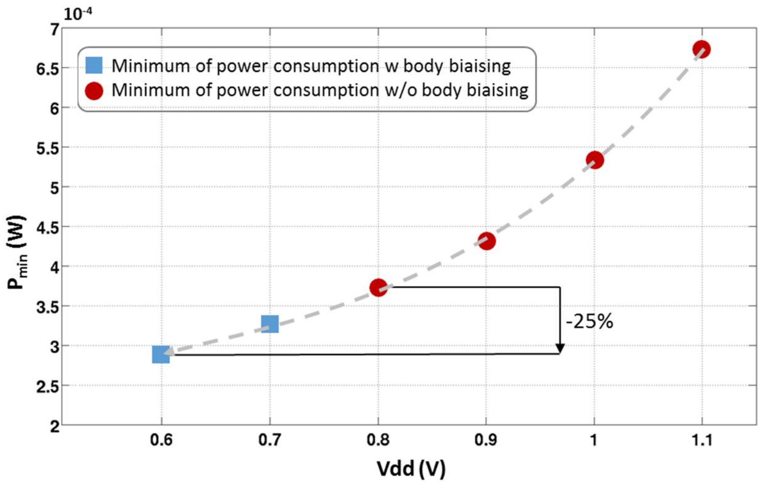
Figure 15 shows the minimum of power consumption (several W
1, W
2, and I
bias) reached for each power supply respecting the design specifications (Gv
LNA = 15 dB, NF
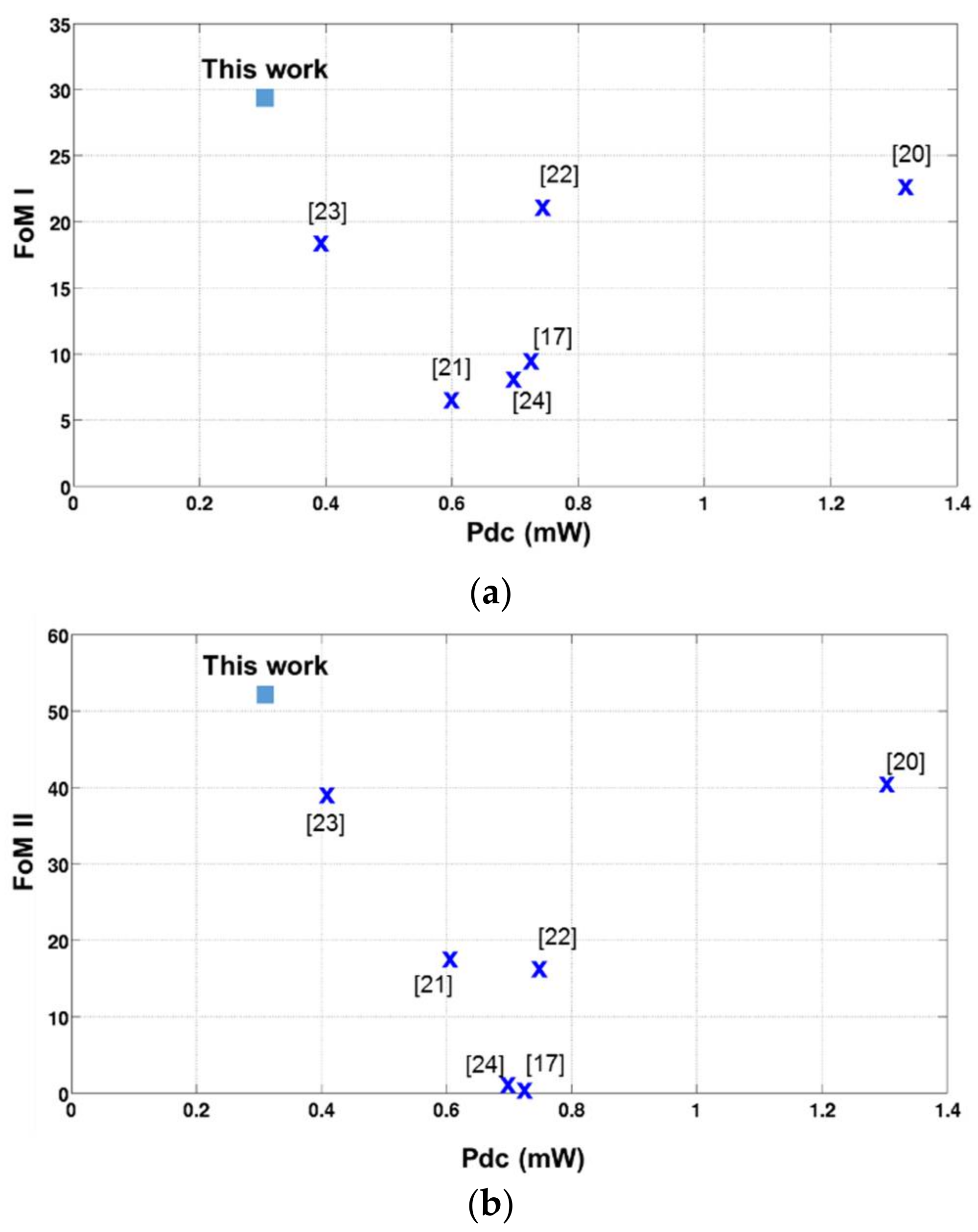
LNA ≤ 7 dB, and S11 ≤ −10 dB). The dots represent the solutions without any back gate biasing. The minimum of power consumption in that case is reached for Vdd = 0.8 V. Beyond this power supply, there is no solution for a correct saturation of the transistors. The power consumption of the LNA at this operating point is 380 µW. This design solution gives a FoM of 25.3 with is over the theoretical FoM aimed in
Section 4. Even without using the body biasing of the FD-SOI technology, this technology enables good design performance making it one of the best FoM of State of the Art LNA.
However, this work shows a way to push further the limitation on the saturation of the transistor thanks to the possibility of lowering the threshold voltage of the transistor with the body biasing. Therefore, when a voltage is applied on the body of the transistor, more design solutions with the same performance are available for a lower power consumption.
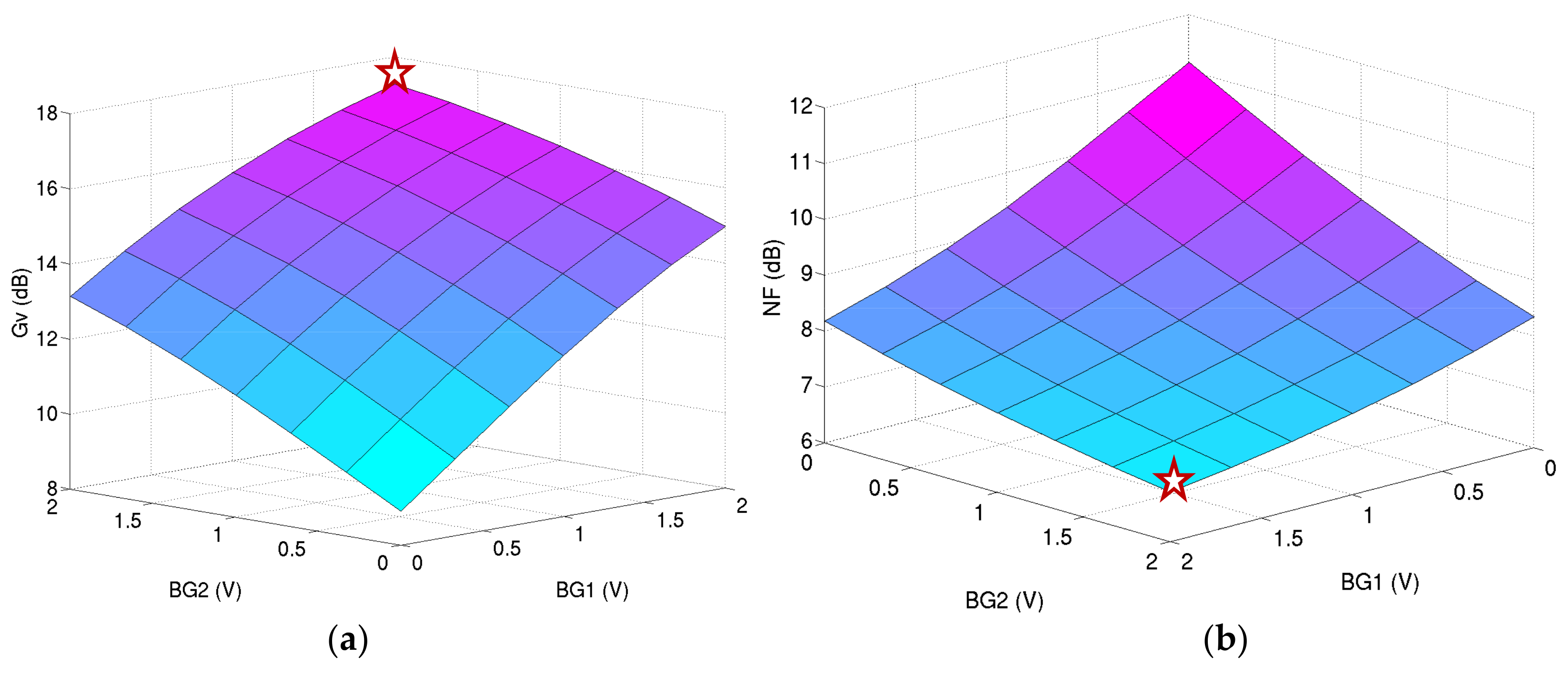
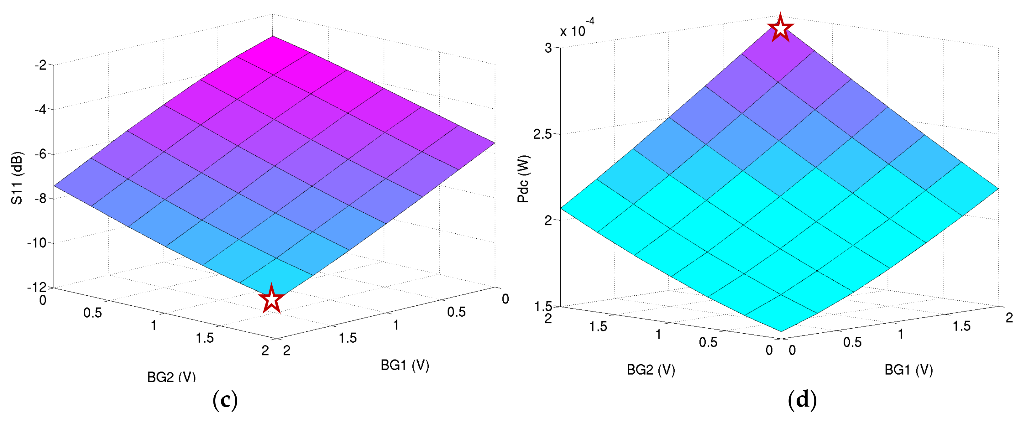
Figure 16 depicts the simulation results for the ULP LNA at a 0.6 V power supply for several voltages on back gate of M1 and M2. It confirms that the performance cannot be maintained without the body biasing at this power supply.
The chosen operating point (plotted red star on
Figure 16) is the lowest power consumption providing the correct performance:
- -
BG1 = 2 V;
- -
BG2 = 2 V; and
- -
Vdd = 0.6 V.
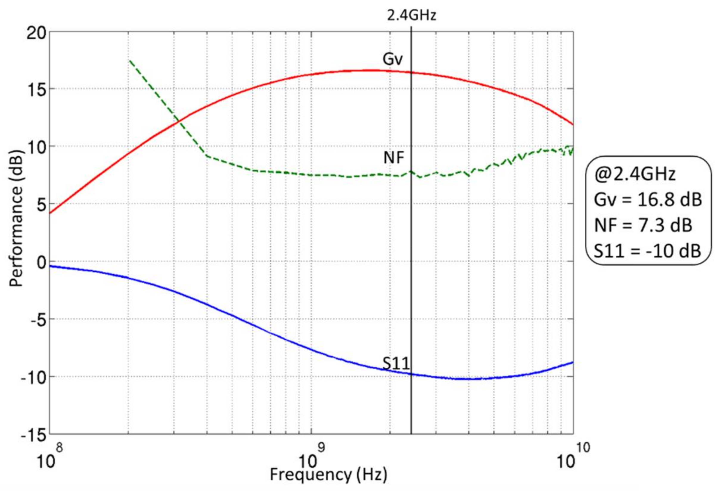
This operating point gives the simulated performance at 2.4 GHz:
- -
S11 = −10.5 dB;
- -
Gv = 17.5 dB;
- -
NF = 6.9 dB; and
- -
Pdc = 300 µW.
By using the body biasing, the threshold voltage of the transistors is decreased and the power supply voltage can thus be reduced to 0.6 V with a back gate voltage of +2 V. More than 25% of the power consumption on the LNA can be saved.
4.3. PVT Degradation Evaluation
As the technology is decreasing to deep submicron processes, the circuit process, voltages and temperature variations can degrade the RF performance of the LNA. The system analysis proposed in
Section 3 validates the needs of a sensitivity of −75 dBm for the low power mode. This threshold has to be guaranteed even with Process Voltage Temperature (PVT) deviations.
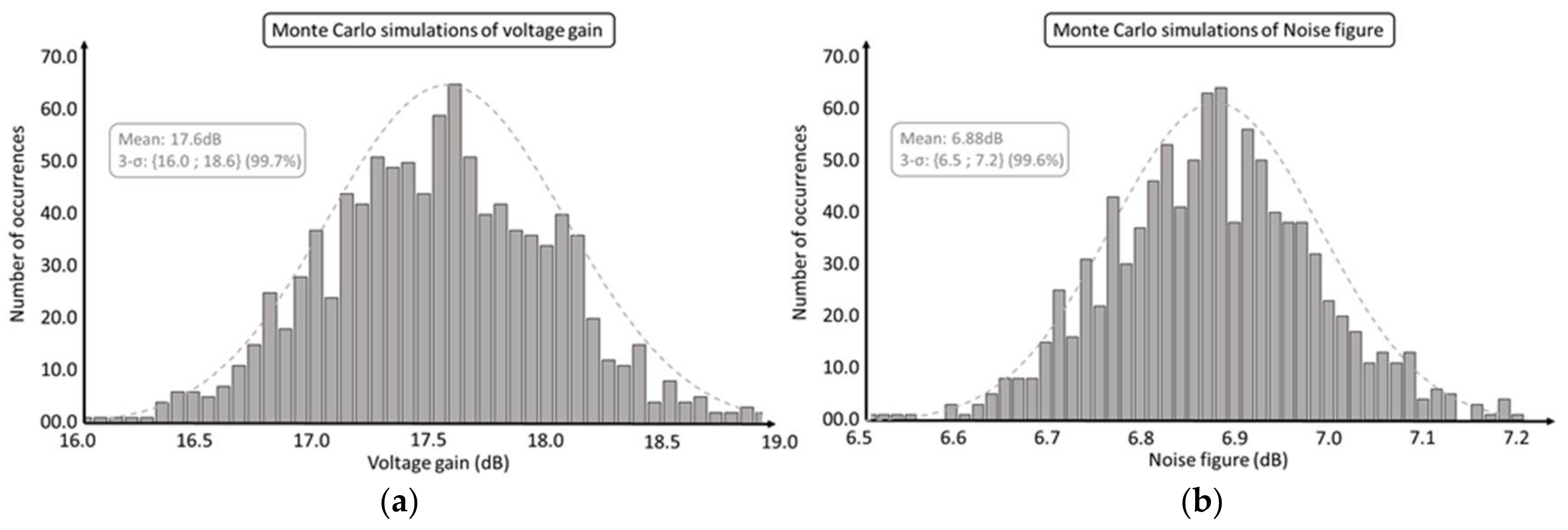
Figure 17 shows the Monte Carlo simulations performed for 1000 occurrences and the extraction of the LNA’s voltage gain and noise figure at 2.4 GHz.
The performance of the LNA at the minimum and maximum of 3-σ Monte Carlo simulations results have been introduced to the system analysis described in
Section 3 in order to evaluate the impact of the PVT variation of the LNA on the receiver’s sensitivity (others blocks of the chain have been considered at fixed performance).
Table 4 presents the worst and best 3-σ Monte Carlo simulations noise figure and voltage gain of the LNA and their impact on the sensitivity of the receiver. The results shows a delta of 1.5 dB on the sensitivity of the receiver. Even for the worst PVT performance deviation, the sensitivity threshold −75 dBm is guaranteed with the design of this LNA.


