Fully Integrated Solar Energy Harvester and Sensor Interface Circuits for Energy-Efficient Wireless Sensing Applications

Abstract
:1. Introduction
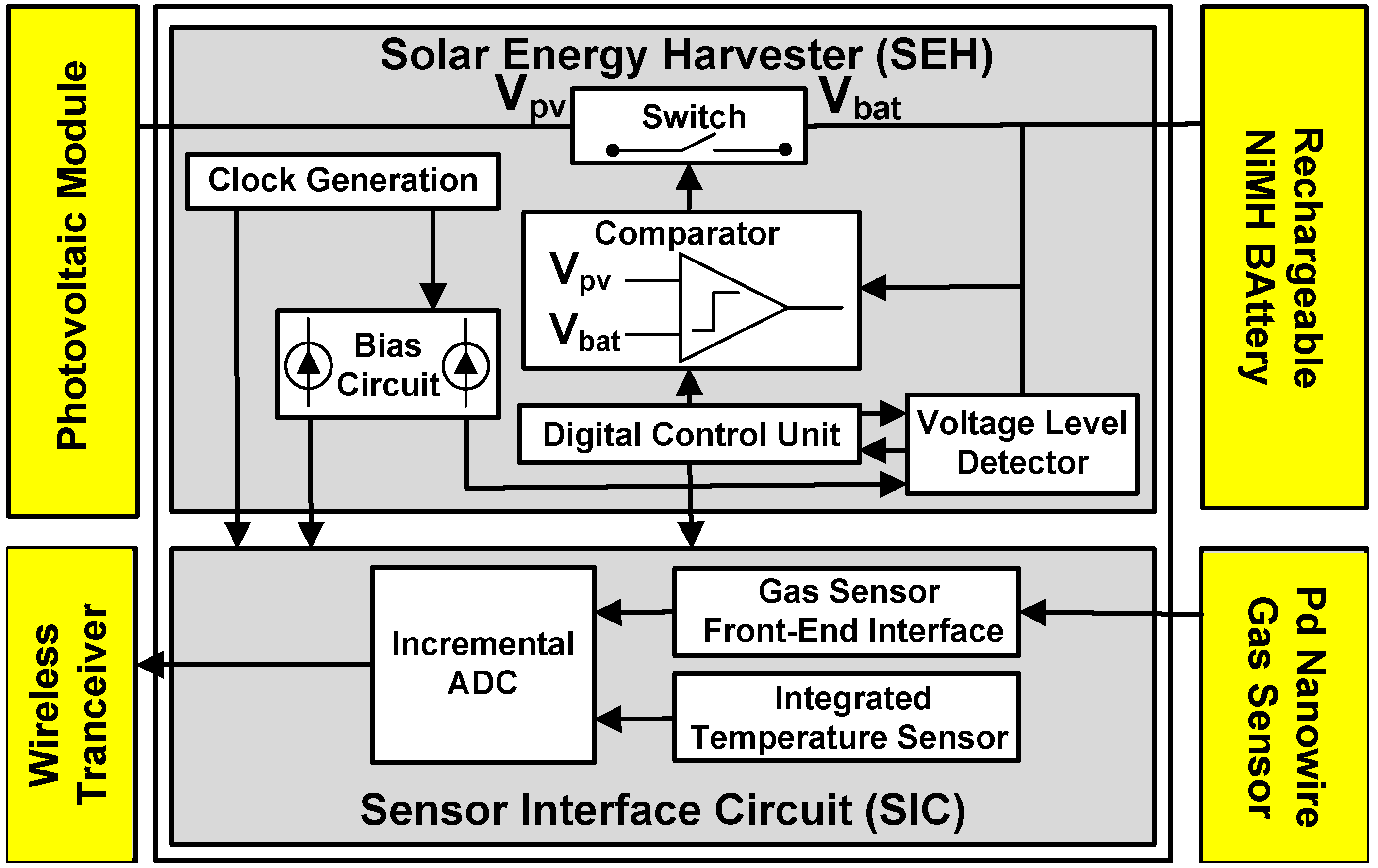
2. System Architecture
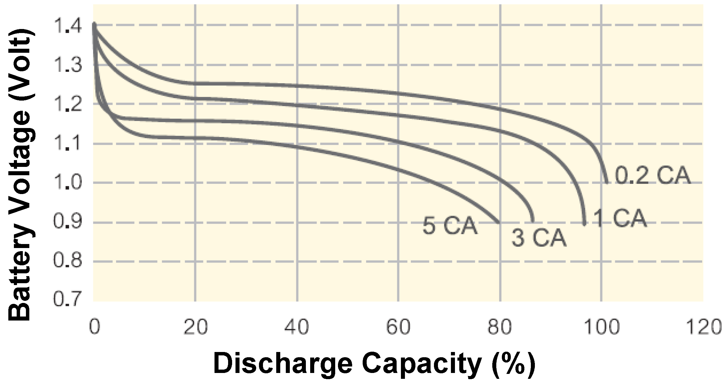
2.1. Energy Storage Option

| Energy Storage Option/Specification | CAP-XX (GZ115F) [10] | Infinite Power Solutions (MEC125) [11] | Varta (V6HR) [2] |
|---|---|---|---|
| Technology | Supercapacitor | Thin film lithium battery | NiMH battery |
| Nominal operating voltage | 2.3 V | 4.1 V | 1.2 V |
| Size | 20 × 15 × 1.25 mm3 | 12.7 × 12.7 × 0.7 mm3 | D: 6.8 mm, H: 2.15 mm |
| Energy capacity | 4 µAh | 200 µAh | 6200 µAh |
| Peak discharge current | 30 A | 7.5 mA | 18 mA |
| Cycle life | 30,000+ hours | 10,000 | 1000 |
2.2. Solar Energy Harvester


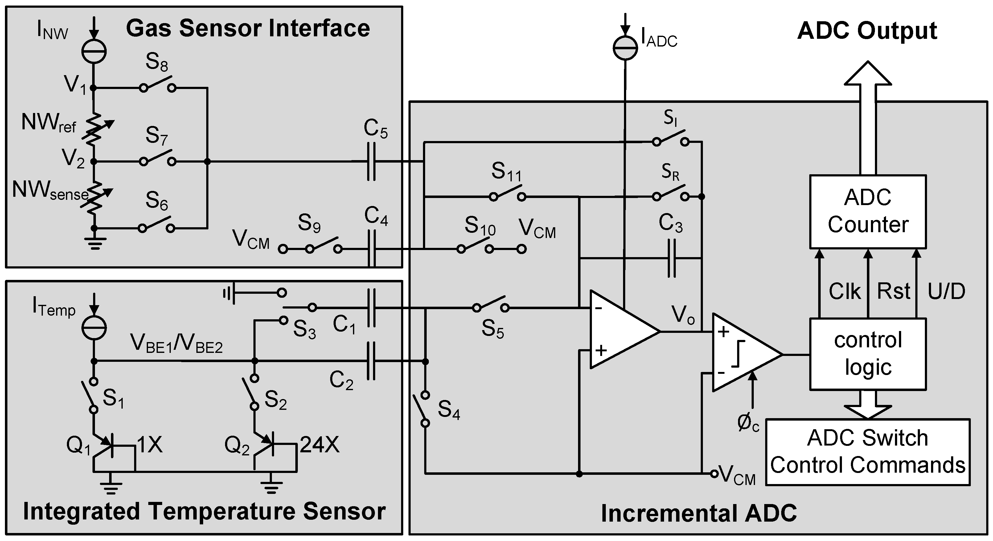
2.3. Sensor Interface Unit
2.4. Wireless Transceiver
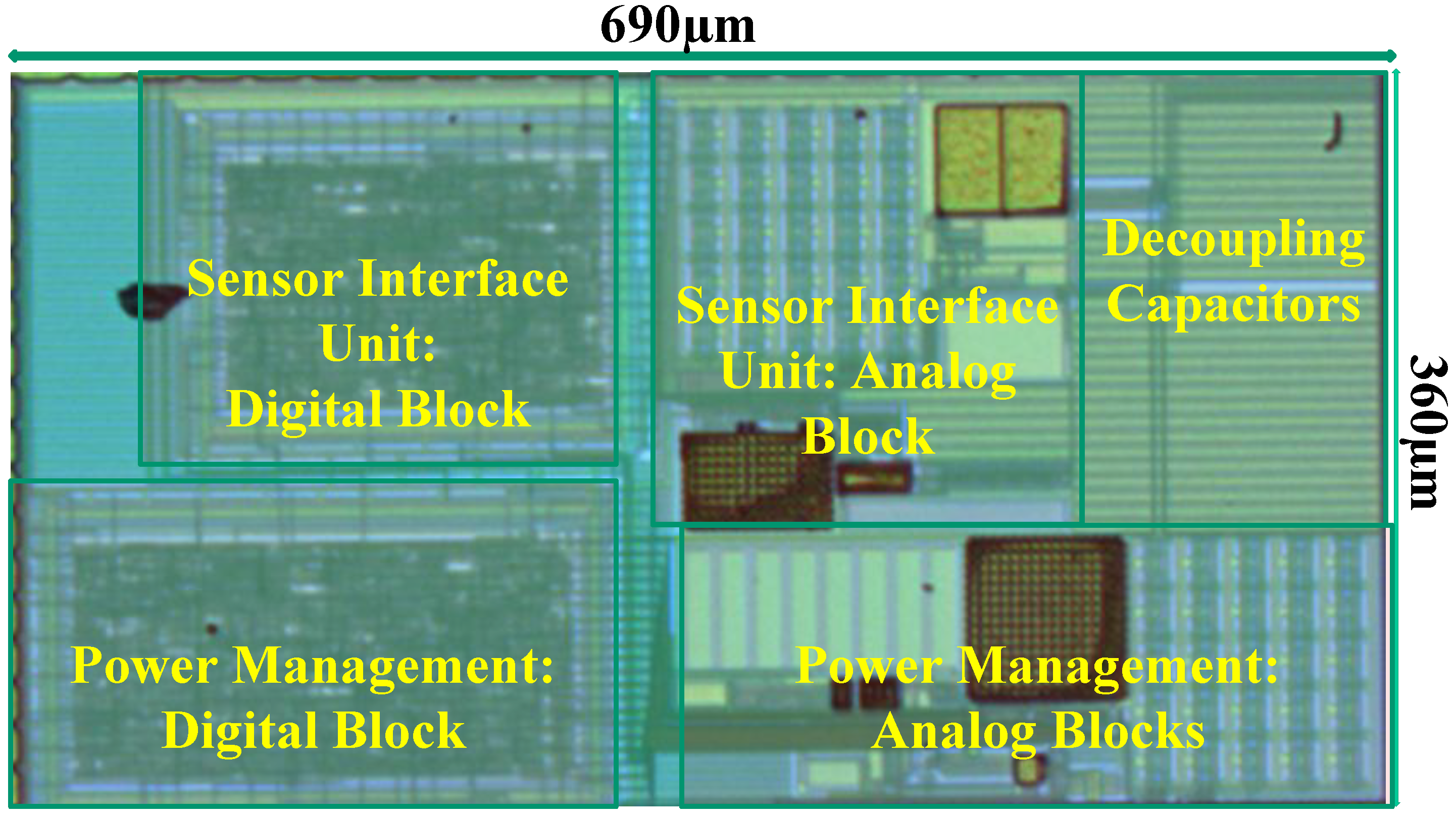
3. System Implementation
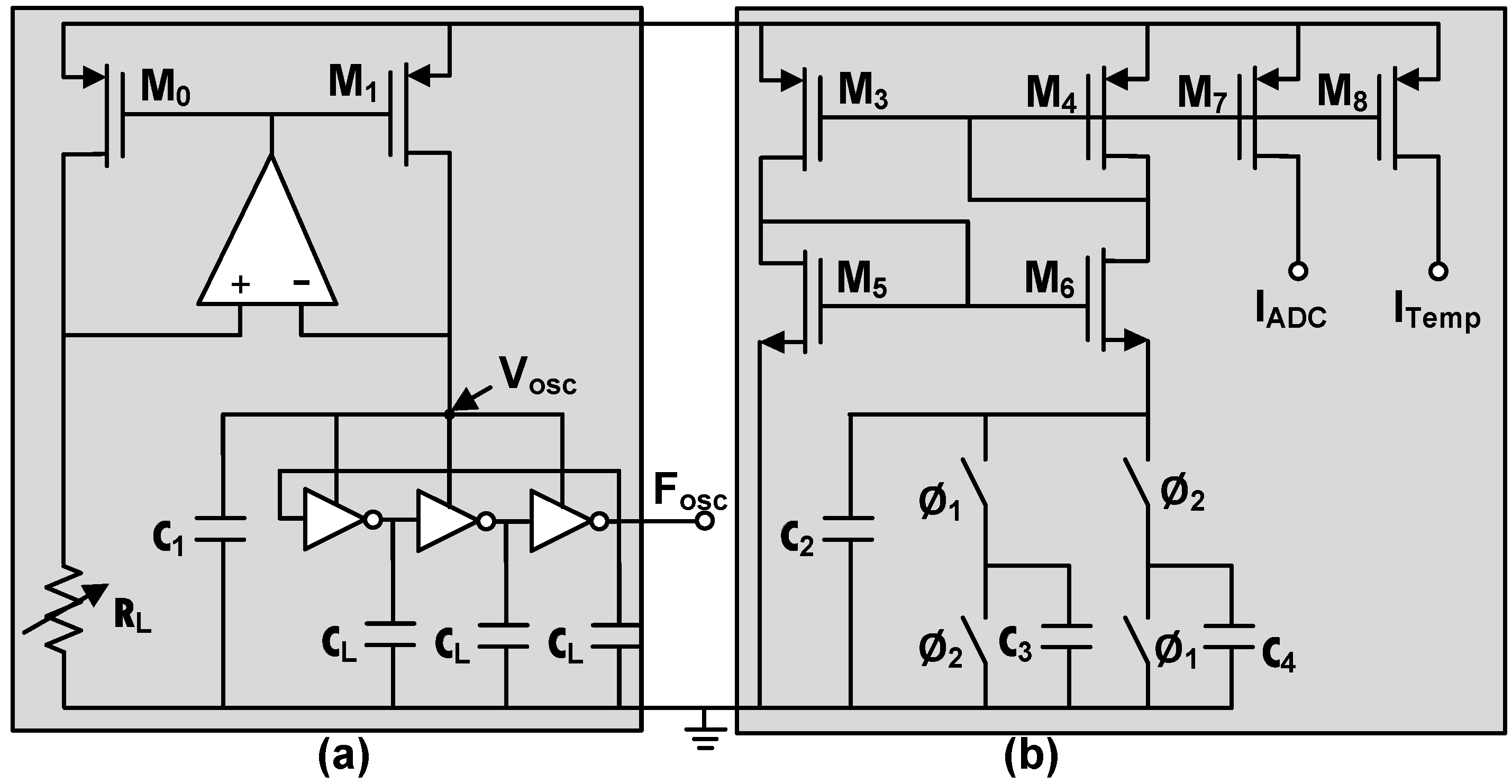
3.1. Solar Energy Harvester
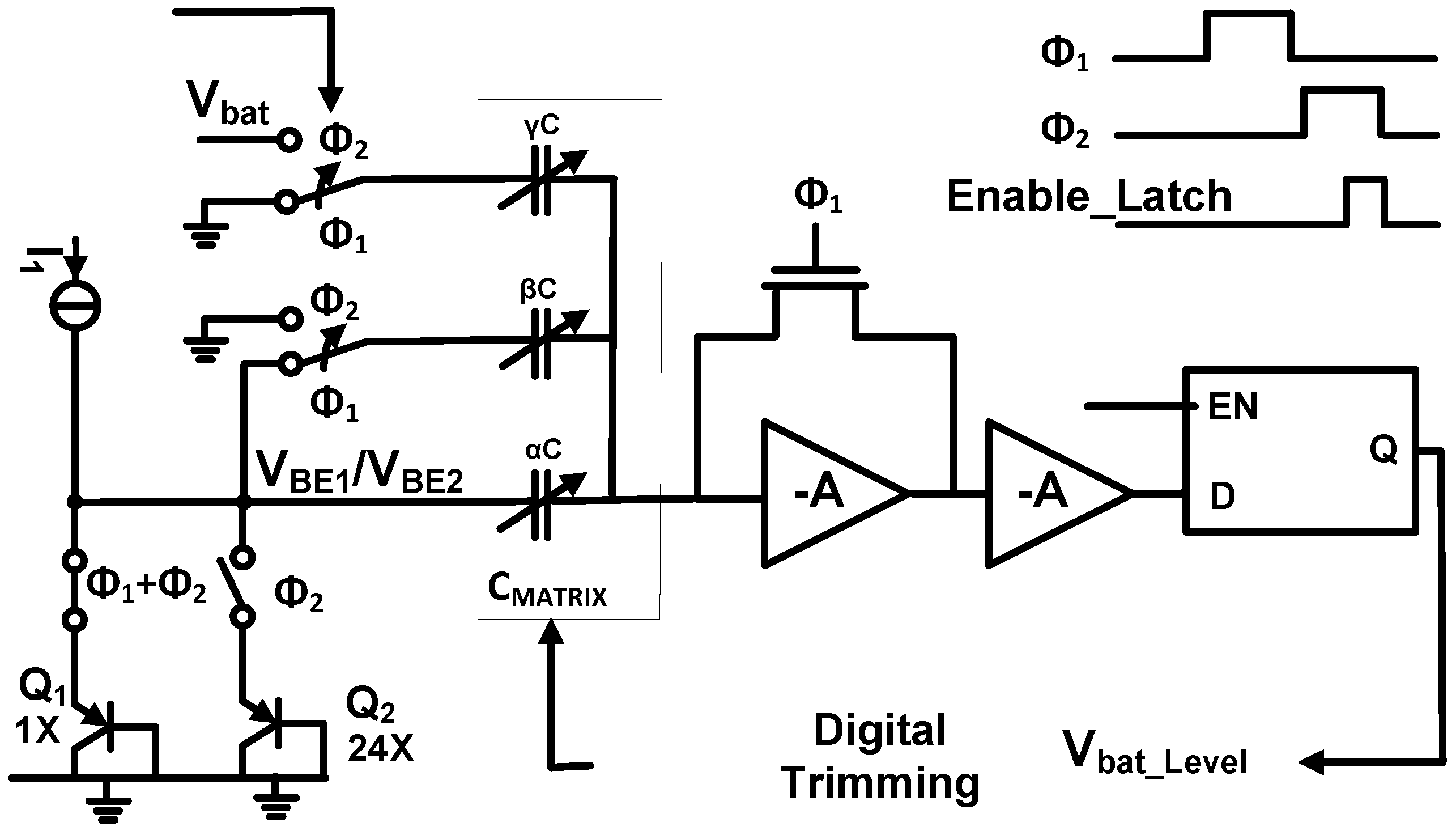

| Voltage Level (VL) | αC Capacitor | βC Capacitor | γC Capacitor |
|---|---|---|---|
| 907 mV (VEOD) | 170 fF | 1230 fF | 230 fF |
| 947 mV (VL0) | 170 fF | 1230 fF | 220 fF |
| 1002 mV (VL1) | 180 fF | 1300 fF | 220 fF |
| 1051 mV (VL2) | 180 fF | 1300 fF | 210 fF |
| 1104 mV (VL3) | 190 fF | 1370 fF | 210 fF |
| 1509 mV (VEOC) | 160 fF | 1160 fF | 130 fF |

| Block | Die Area (µm2) | Active Power (nW) | Average Power (nW) | |
|---|---|---|---|---|
| Clock generator | 14,400 | 165 | 165 | |
| Digital control unit | 38,115 | 90 | 90 | |
| Bias circuit (10 nA) | 2,832 | 35 | 35 | |
| Comparator | 759 | 55 | <1 | |
| Level detector | 31,960 | 520 | <1 | |
| SCBM | 6,300 | 640 | <1 | |
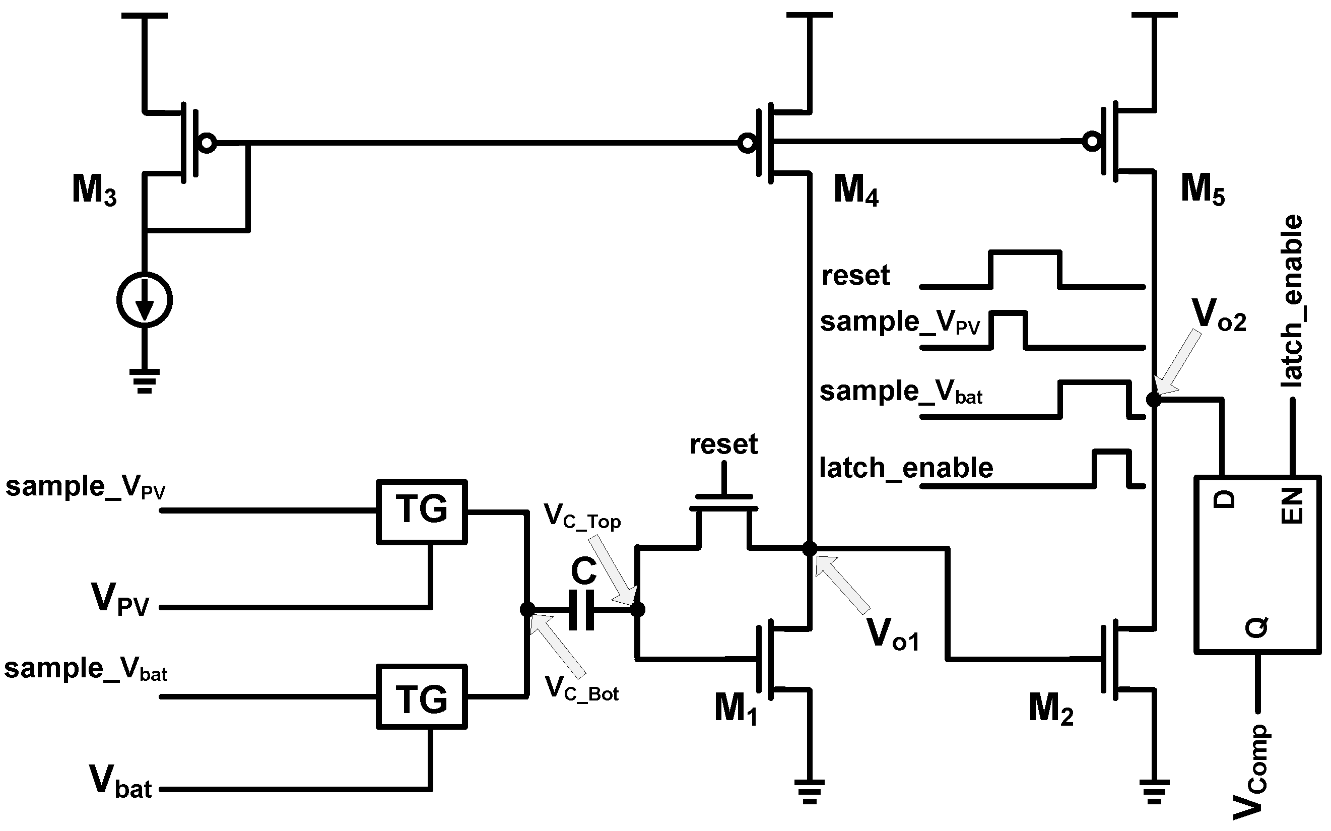
3.2. Sensor Interface Circuit

4. System Integration and Performance

| Block | SL3 | SL2 | SL1 | SL0 | ||
|---|---|---|---|---|---|---|
| Detected Vbat during 5CA discharge (mV) | 1,104 | 1,051 | 1,002 | 947 | ||
| Battery discharge capacity (%) | <20% | <50% | <65% | <75% | ||
| Battery threshold voltage (V) | Measured | 1.114 | 1.055 | 1.003 | 0.955 | |
| Simulated | 1.122 | 1.063 | 1.010 | 0.962 | ||
| Clock frequency (kHz) | Measured | 950 | 488 | 249 | 127 | |
| Simulated | 980 | 502 | 257 | 132 | ||
| Time interval of sensing and data transmission (seconds) | 15 | 30 | 60 | 120 | ||
| Power consumption of clock generator (nW) | 165 | 85 | 44 | 23 | ||
| Power consumption of digital control unit (nW) | 90 | 46 | 24 | 13 | ||
| Average power consumption of energy harvester (nW) | Measured | 346 | 210 | 142 | 103 | |
| Simulated | 293 | 169 | 106 | 74 | ||
| Average power consumption of sensor interface circuit (nW) | Measured | 1730 | 1120 | 790 | 640 | |
| Simulated | 1360 | 870 | 625 | 500 | ||
| Average power consumption of the integrated circuit (nW) | 2076 | 1330 | 932 | 707 | ||
| Average current consumption of gas sensor bias circuit (µA) | 4.67 | 2.33 | 1.16 | 0.58 | ||
| Average current consumption of the wireless transceiver (µA) | 9.4 | 7.7 | 6.6 | 5.55 | ||
| Average current consumption of the complete system (µA) | 16 | 11 | 8.5 | 6.7 | ||
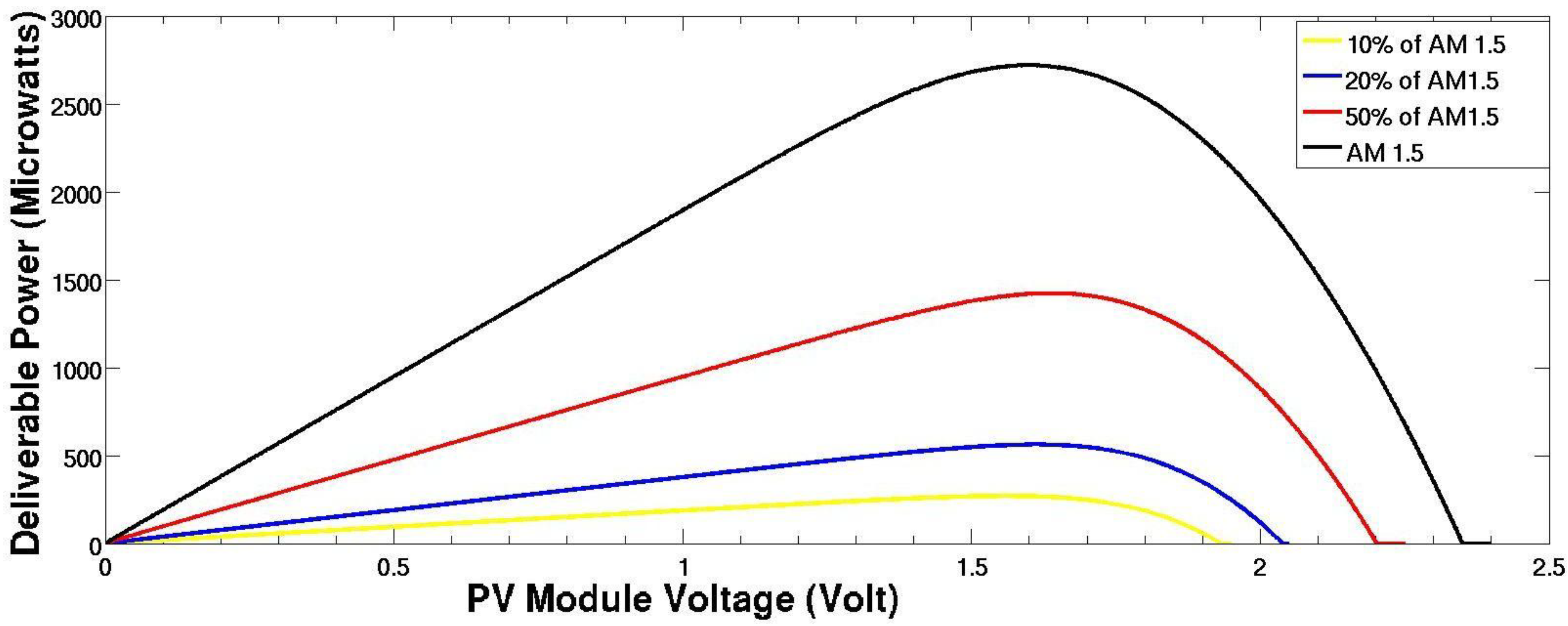
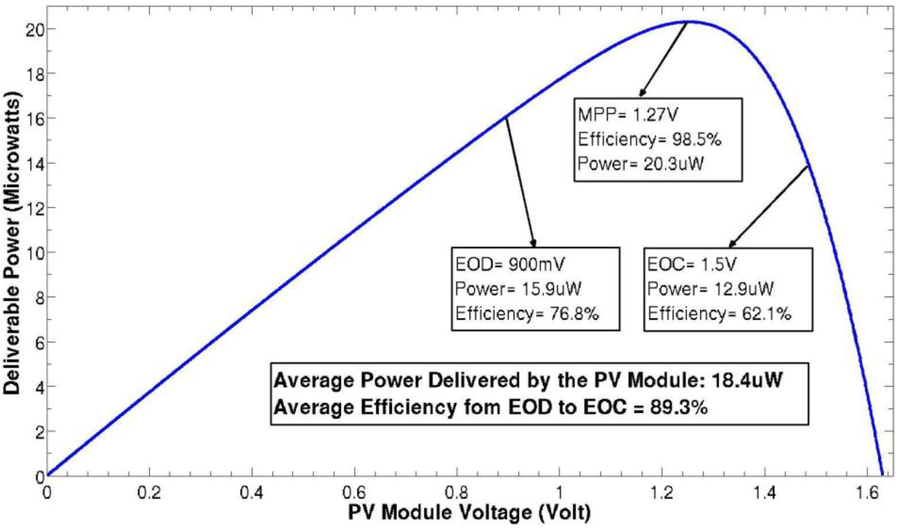
| Illumination Level | Vmpp (V) | Pmpp (µW) | Pcharge (µW) | Efficiency |
|---|---|---|---|---|
| 100% of AM1.5 | 1.586 | 2,718 | 2,240.8 | 82% |
| 50% of AM1.5 | 1.622 | 1,422 | 1,127.3 | 79.2% |
| 20% of AM1.5 | 1.604 | 561.6 | 448.4 | 79.8% |
| 10% of AM1.5 | 1.549 | 269.5 | 221.4 | 82.1% |
| 1% of AM1.5 | 1.289 | 20.3 | 18.4 | 89.3% |

5. Conclusions
Acknowledgments
References
- Jia, G.; Steglich, M.; Sill, I.; Falk, F. Core-shell heterojunction solar cells on silicon nanowire arrays. Sol. Energy Mater. Sol. Cells 2012, 96, 226–230. [Google Scholar] [CrossRef]
- Varra V6HR Datasheet. Available online: http://www.varta-microbattery.com (accessed on 3 December 2012).
- Toumaz TZ1053 Datasheet. Available online: http://www.toumaz.com/page.php?page=telran (accessed on 3 December 2012).
- Chen, G.; Ghaed, H.; Haque, R.; Wieckowski, M.; Yejoong, K.; Gyouho, K.; Fick, D.; Daeyeon, K.; Mingoo, S.; Wise, K.; Blaauw, D.; Sylvester, D. A Cubic-Millimeter Energy-Autonomous Wireless Intraocular Pressure Monitor. In Proceedings of IEEE International Solid-State Circuits Conference, San Francisco, CA, USA, 20–24 February 2011; pp. 310–312.
- Qiu, Y.; Liempd, C.V.; Veld, B.O.H.; Blanken, P.G.; Hoof, C.V. 5 μW-to-10 mW Input Power Range Inductive Boost Converter for Indoor Photovoltaic Energy Harvesting with Integrated Maximum Power Point Tracking Algorithm. In Proceedings of IEEE International Solid-State Circuits Conference, San Francisco, CA, USA, 20–24 February 2011; pp. 118–120.
- Khosro Pour, N.; Krummenacher, F.; Kayal, M. Fully integrated ultra-low power management system for micro-power solar energy harvesting applications. Electron. Lett. 2012, 48, 338–118. [Google Scholar] [CrossRef]
- Offermans, P.; Tong, H.D.; Van Rijn, C.J.M.; Merken, P.; Brongersma, S.H.; Crego-Calama, M. Ultralow-power hydrogen sensing with single palladium nanowires. Appl. Phys. Lett. 2009, 94, 223110–223113. [Google Scholar]
- Van der Bent, J.F.; van Rijn, C.J.M. Ultra low power temperature compensation method for palladium nanowire grid. Procedia Eng. 2010, 5, 184–187. [Google Scholar] [CrossRef]
- Pour, N.K.; Krummenacher, F.; Kayal, M. A Miniaturized Autonomous Microsystem For Hydrogen Gas Sensing Applications. In Proceedings of IEEE 10th International New Circuits and Systems Conference, Montreal, Canada, 17–20 June 2012; pp. 201–204.
- Cap-XX Co. Website. Available online: http://www.cap-xx.com (accessed on 3 December 2012).
- InfinitePowerSolutions Co. Website. Available online: http://www.infinitepowersolutions.com (accessed on 3 December 2012).
- Lu, C.; Raghunathan, V.; Roy, K. Micro-Scale Energy Harvesting: A System Design Perspective. In Proceedings of 15th Asia and South Pacific Design Automation Conference (ASP-DAC), Taipei, Taiwan, 18–21 January 2010; pp. 89–94.
- Markus, J.; Silva, J.; Temes, G.C. Theory and applications of incremental ΔΣ converters. IEEE Trans. Circuits Syst. 2004, 51, 678–690. [Google Scholar] [CrossRef]
- Zarlink ZL70250 Datasheet. Available online: http://www.zarlink.com/zarlink (accessed on 3 December 2012).
- Esram, E.; Chapman, P.L. Comparison of photovoltaic array maximum power point tracking techniques. IEEE Trans. Energy Conver. 2007, 22, 439–449. [Google Scholar] [CrossRef]
- Lu, C.; Raghunathan, V.; Roy, K. Maximum power point considerations in micro-scale solar energy harvesting systems. In Proceedings of IEEE International Symposium on Circuits and Systems (ISCAS), Paris, France, 30 May–2 June 2010; pp. 273–276.
- Pastre, M.; Krummenacher, F.; Kazanc, O.; Khosro Pour, N.; Pace, C.; Rigert, S.; Kayal, M. A solar battery charger with maximum power point tracking. In Proceedings of 18th IEEE International Conference on ElectronicsCircuits and Systems (ICECS), Beirut, Lebanon, 11–14 December 2011; pp. 394–397.
- Pastre, M.; Krummenacher, F.; Robortella, R.; Simon-Vermot, R.; Kayal, M. A fully integrated solar battery charger. In Proceedings of Joint IEEE North-East Workshop on Circuits and Systems and TAISA Conference, Toulouse, France, 28 June–1 July 2009; pp. 1–4.
- Pertijs, M.A.P.; Makinwa, K.A.A.; Huijsing, J.H. A CMOS smart temperature sensor with a 3σ inaccuracy of ±0.1 °C from −55 °C to 125 °C. IEEE J. Solid State Circuits 2005, 40, 2805–2815. [Google Scholar] [CrossRef]
© 2013 by the authors; licensee MDPI, Basel, Switzerland. This article is an open access article distributed under the terms and conditions of the Creative Commons Attribution license (http://creativecommons.org/licenses/by/3.0/).
Share and Cite
Khosro Pour, N.; Krummenacher, F.; Kayal, M. Fully Integrated Solar Energy Harvester and Sensor Interface Circuits for Energy-Efficient Wireless Sensing Applications. J. Low Power Electron. Appl. 2013, 3, 9-26. https://doi.org/10.3390/jlpea3010009
Khosro Pour N, Krummenacher F, Kayal M. Fully Integrated Solar Energy Harvester and Sensor Interface Circuits for Energy-Efficient Wireless Sensing Applications. Journal of Low Power Electronics and Applications. 2013; 3(1):9-26. https://doi.org/10.3390/jlpea3010009
Chicago/Turabian StyleKhosro Pour, Naser, François Krummenacher, and Maher Kayal. 2013. "Fully Integrated Solar Energy Harvester and Sensor Interface Circuits for Energy-Efficient Wireless Sensing Applications" Journal of Low Power Electronics and Applications 3, no. 1: 9-26. https://doi.org/10.3390/jlpea3010009