Article

Analog Encoding Voltage—A Key to Ultra-Wide Dynamic Range and Low Power CMOS Image Sensor

1
The VLSI Systems Center, LPCAS, Ben-Gurion University, P.O.B. 653, Be'er-Sheva 84105, Israel
2
Department of Electrical and Computer Engineering, Bar Ilan University, Ramat Gan, 52100, Israel
3
Department of Electrical Engineering, University of Calgary, Alberta T2N 1N4, Canada
*
Author to whom correspondence should be addressed.
J. Low Power Electron. Appl. 2013, 3(1), 27-53; https://doi.org/10.3390/jlpea3010027
Submission received: 22 November 2012 / Revised: 29 January 2013 / Accepted: 22 February 2013 / Published: 22 March 2013
(This article belongs to the Special Issue Energy Efficient Sensors and Applications)

Abstract

:
Usually Wide Dynamic Range (WDR) sensors that autonomously adjust their integration time to fit intra-scene illumination levels use a separate digital memory unit. This memory contains the data needed for the dynamic range. Motivated by the demands for low power and chip area reduction, we propose a different implementation of the aforementioned WDR algorithm by replacing the external digital memory with an analog in-pixel memory. This memory holds the effective integration time represented by analog encoding voltage (AEV). In addition, we present a “ranging” scheme of configuring the pixel integration time in which the effective integration time is configured at the first half of the frame. This enables a substantial simplification of the pixel control during the rest of the frame and thus allows for a significantly more remarkable DR extension. Furthermore, we present the implementation of “ranging” and AEV concepts on two different designs, which are targeted to reach five and eight decades of DR, respectively. We describe in detail the operation of both systems and provide the post-layout simulation results for the second solution. The simulations show that the second design reaches DR up to 170 dBs. We also provide a comparative analysis in terms of the number of operations per pixel required by our solution and by other widespread WDR algorithms. Based on the calculated results, we conclude that the proposed two designs, using “ranging” and AEV concepts, are attractive, since they obtain a wide dynamic range at high operation speed and low power consumption.

1. Introduction

Extending the dynamic range (DR) of a CMOS image sensor’s (CIS) remains one of the challenges to be faced in designing an effective versatile sensor. Improvement of image capture capability can be done either by reducing the noise floor (NF) of the sensor [1,2,3] or by extending its saturation toward higher light intensities. Most of the cases that are reported in the literature give solutions which focus on extending the DR toward high light intensities. There are numerous solutions that have been proposed throughout the years [4,5,6,7,8,9,10,11,12,13,14,15,16,17,18,19,20,21,22,23,24,25,26,27]. However, the majority of the proposed WDR solutions have used an external memory, which significantly increased their area and power consumption and, as a result, their cost.
Examples of using a digital memory can be found in a large variety of solutions [8] such as (a) multimode sensors that have a linear and a logarithmic response at dark and bright illumination levels, respectively [9]; (b) clipping sensors, in which a well capacity adjustment method is applied [10]; (c) frequency-based sensors, in which the sensor output is converted into a pulse frequency [12]; (d) time-to-first spike (TFS) sensors, in which the image is processed according to the time the pixel was detected as saturated [‎9]; (e) sensors with global control over the integration time, in which the pixel integrates for a set of exposures regardless of its input light intensity [15]; and (f) sensors with autonomous control over the integration time (multiple resets), in which each pixel has control over its own exposure period [16,17,18]. In the aforementioned designs the memories were used to store the possible pixel outputs or the DR extension data. The reason for using a memory is that the data processing becomes more straightforward, i.e., it is easy to split the processing into several independent stages and to store the intermediate results. However, in such a case, the overall processing time and power increase.
Nevertheless, we can find memory free WDR solutions as well. For example, in [19] a TFS algorithm implementation is described, where, instead of using a digital code to represent the saturation time, the authors paired each time slot with a certain voltage value that was subsequently converted into corresponding digital pixel value. This solution unfortunately suffers from the reduced sensitivity throughout the whole DR [8].
It is especially interesting to look into the free memory solutions in [20,21], which are based upon the global control over the integration time, since this category is the most widely spread in the industry. The memory can be omitted if there are two exposures as will be shown later on. However, using two exposures causes a substantial signal to noise ratio (SNR) drop in the mid-tones, which can necessitate subsequent image processing.
With autonomous control over the integration time category, the memory emerges as the main cause for the increase in both the complexity and the cost of the solution. Attempts to dump the memory in this category have been undertaken as well. In [22] a successful memory free solution was presented. That solution was based upon a very simple pixel structure, in which the pixel integration time value was encoded in voltage and stored on the intra-pixel capacitance. But, since the same capacitance was also used for readout of the intermediate pixel values, the stored integration times were continuously overwritten and refreshed over and over again slowing the sensor operation.
In this work, we present two novel concepts in “ranging” and analog encoding voltage (AEV) for design of low power, high speed, memory free WDR sensors with autonomous control over integration time. According to the “ranging” concept, the pixel signal is “coarsely” quantized at the beginning of the frame, and the final “fine” quantization takes place at the end of the frame. Generated data in the “coarse” quantization is stored as analog encoding voltage (AEV) inside each pixel on a separate capacitance, and this controls the pixel integration throughout the frame. Since we use different capacitances for a photo-induced signal and for an (AEV), the data processing becomes very simple and fluent. At the end of the frame, both of the two analog values, the photo-generated charge and the AEV, are merged through an analog to digital A/D conversion to a final digitized pixel value.
In addition, we present two designs which implement the “ranging” and AEV concepts. The designs are thoroughly described from the schematic to the layout. Moreover, we present the post-layout simulation results of the second design, showing successful DR extension up to 170 dBs. To illustrate the effectiveness of the proposed solutions, we perform a qualitative comparison with other published solutions and show that eventually our solutions are optimized for low power WDR imaging.
The presented work is organized as follows: Section 2 introduces our solutions, Section 3 presents the comparison of a number of operations in several types of WDR solutions, and Section 4 concludes the study. Following the last section, there are two Appendixes, namely A and B. They include the detailed considerations of pixel swing segmentation and signal to noise (SNR) considerations, respectively. In this way, the overall concept becomes clearer and no important design consideration is omitted.

2. WDR Solution Based upon Ranging and AEV

2.1. Problem Definition and Proposed Solution

The solution we have used for the DR extension is called the autonomous control over the integration time (multiple resets). None of the pixels in this solution are classic 3T’s, because this enables individual pixel reset via an additional transistor [8]. During the frame the outputs of a selected row are read nondestructively through the regular output chain. Then they are compared with an appropriate threshold at certain time points by comparators, which are found at a separate unit outside the pixel array. If a pixel value exceeds the threshold, a reset is given at that time point to that pixel. The binary information concerning the reset being applied or not is saved in a digital storage, in order to enable proper scaling of the value read. This enables the pixel value to be described as a floating-point representation, wherein the exponent will describe the scaling factor for the actual integration time, while the mantissa will be the regular A/D output. In this way the actual pixel value would be:
Jlpea 03 00027 i001
where Vpixel is the actual pixel value, Mpixel is the analog or digitized output value that has been read out at the end of the frame, X is a chosen constant, 2, for instance. EXP is the exponent value, which describes the scaling factor, i.e., the specific part of the integration time the pixel actually integrated without being saturated.
The bottleneck of the basic solution is that bits representing the EXP are generated during the integration sequentially; hence, after the generation of the subsequent bit, a digital memory should be refreshed. As the number of pixel rows increase, the time that can be allocated to EXP bits’ generation becomes more limited. The restrictions on the DR extension vary according to the mode of sensor operation: rolling or global shutter. This is more obvious in the rolling shutter, wherein the integration in the successive rows is skewed, so there is more time for DR processing. On the other hand, in the global shutter sensor, wherein the integration starts simultaneously in all rows, the processing times are substantially reduced. Therefore, the solution that we propose is targeted mainly for the global shutter sensor.

2.2. The Proposed Solution

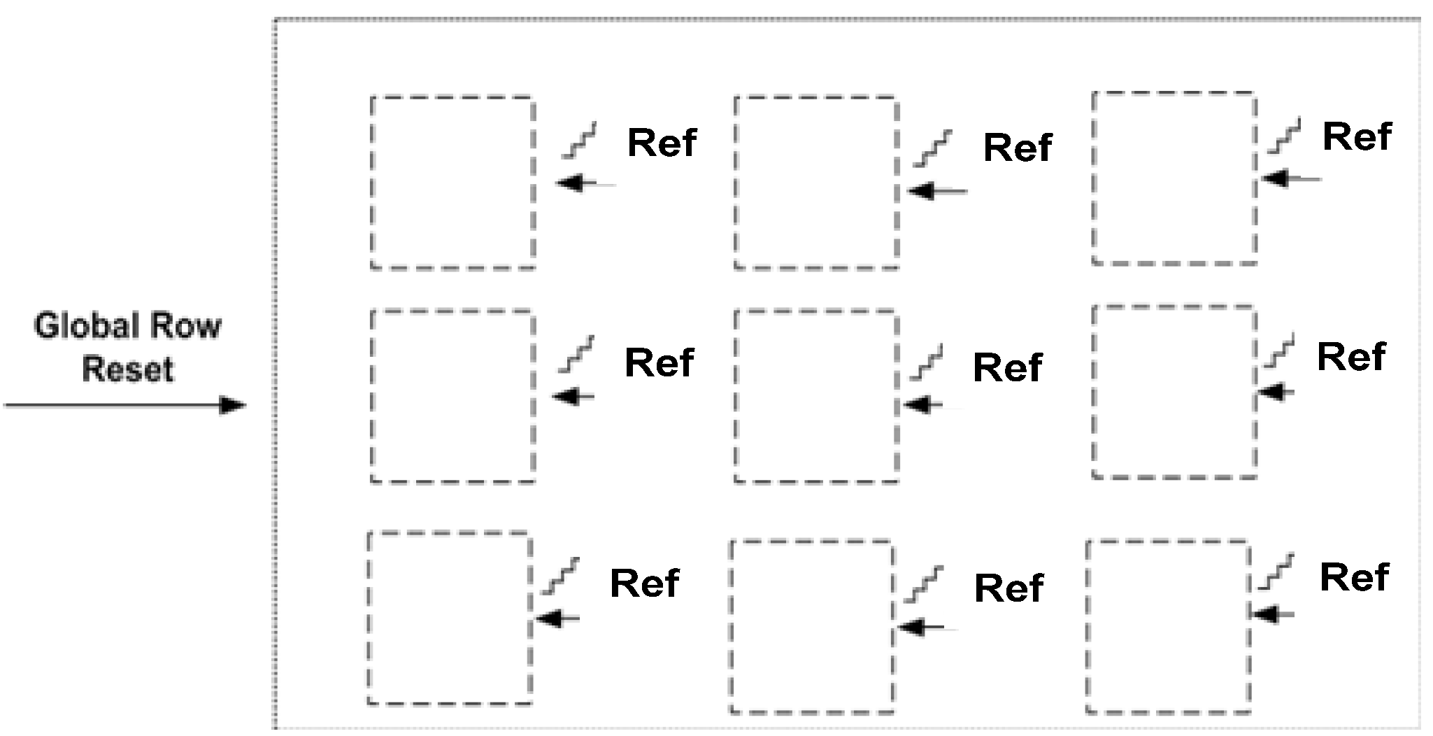
Our solution is based upon “ranging” and AEV concepts. The purpose of this solution is to reduce DR processing times and to omit the memory unit. In addition, we have presented the solution architecture and the flow.
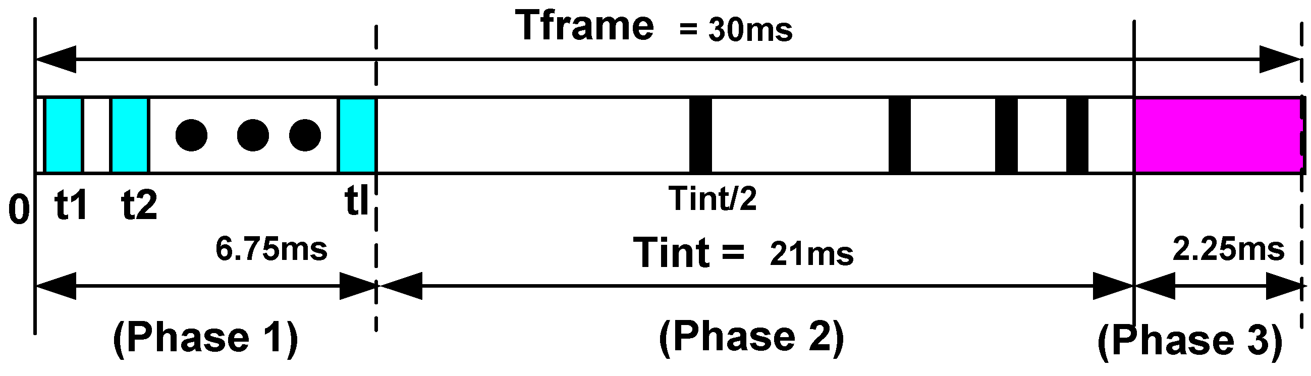
We have divided the WDR algorithm into three phases (Figure 1). During Phase 1, the 
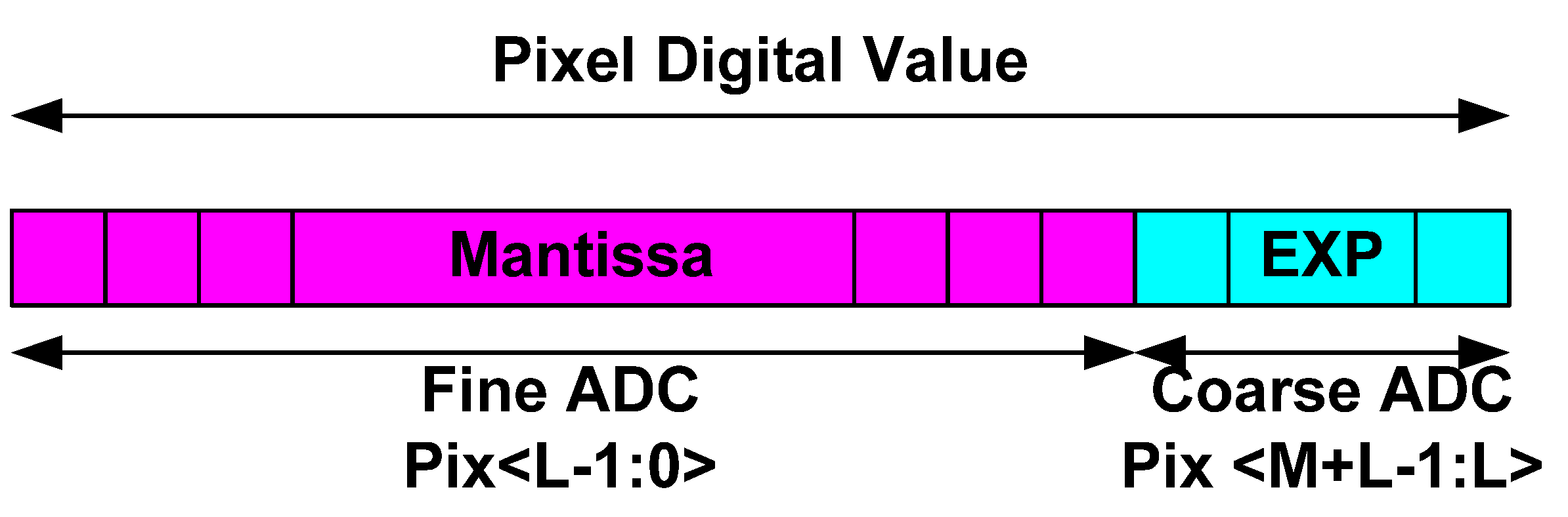
EXP values are produced and memorized inside each pixel in a format of analog encoding voltage AEV. This assignment, which precedes the saturation checks, is called “ranging”, since it “coarsely” quantizes [23] the pixel signal. In fact, the 
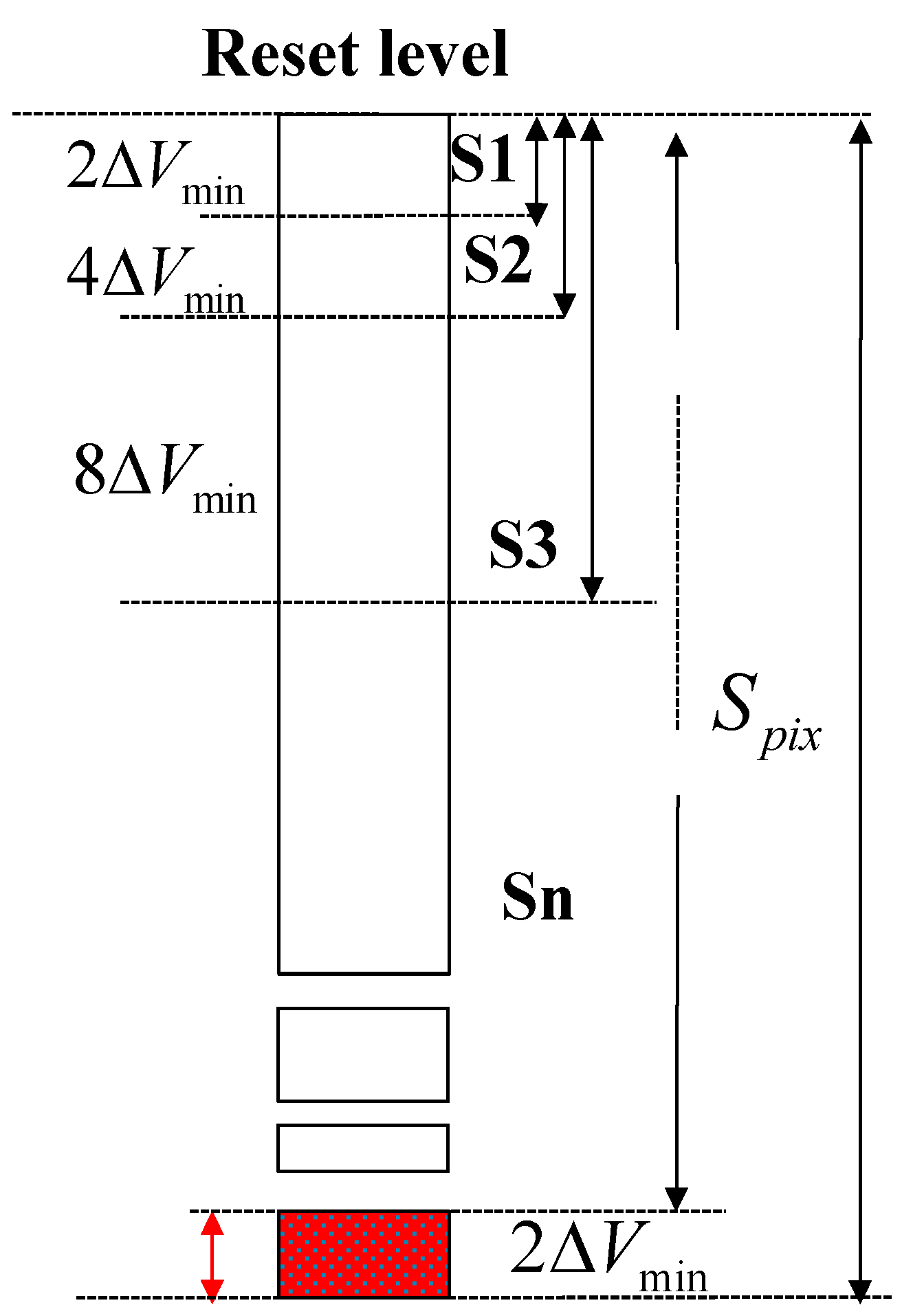
AEV value produced in this quantization, contains the most significant bits of pixel signal Pix<M + L − 1:L> (Figure 2); whereas the Mantissa obtained at the end of the next phase contains the least significant bits Pix<L − 1:0>. In this way, each pixel is given its valid integration time for the current frame before the saturation checks start.
Figure 1. Three Phases of the proposed WDR algorithm.
Jlpea 03 00027 g001
During Phase 2, the pixel integrates in accordance with its AEV. Since the integration time is already known, there is no need to retrieve the last reset information or to refresh information for the current check as was performed in our previous solutions; we merely compare the AEV to the global reference. In case the AEV is below the reference, the pixel will be reset; if not, the pixel will remain untouched till the next frame.
Figure 2. Digital Pixel Value: Mantissa and the EXP bits.
Jlpea 03 00027 g002
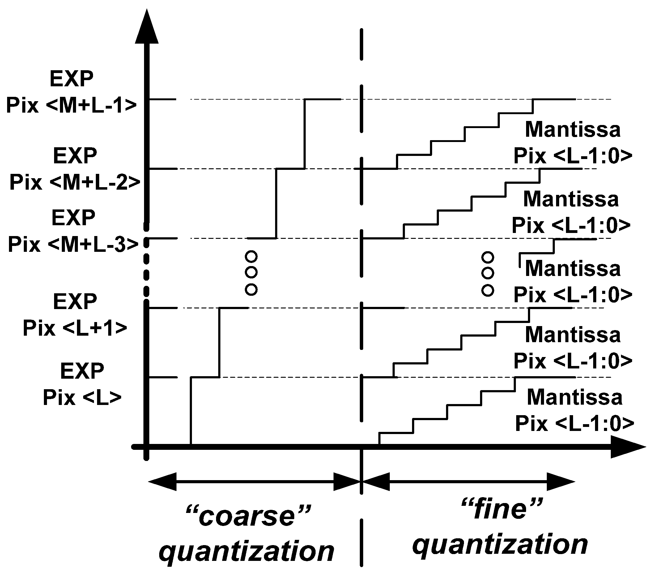
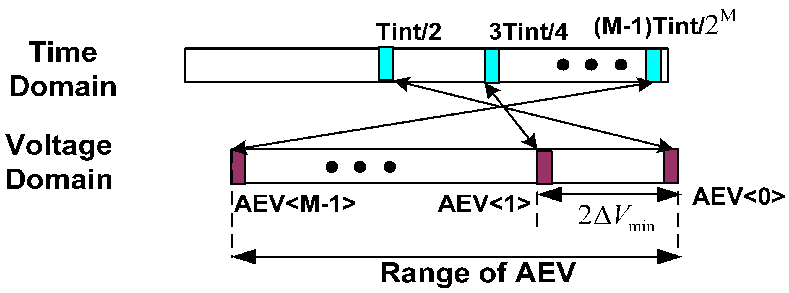
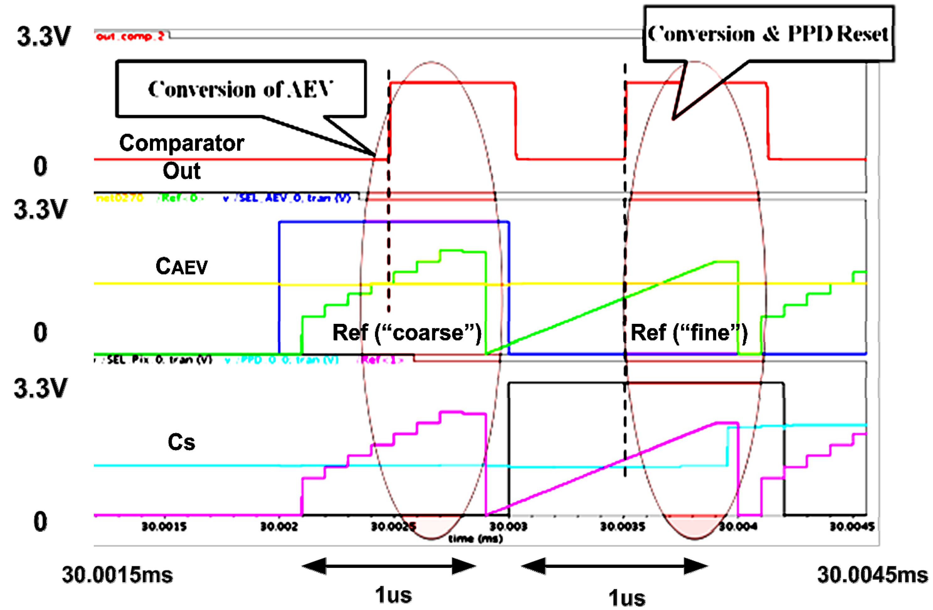
During Phase 3, both the AEV and Mantissa are digitized in a single slope analog to a digital conversion (ADC) (Figure 3). For this purpose, the AEV and Mantissa are read separately and converted with different resolutions. The AEV is digitized with a “coarse” resolution; whereas the Mantissa is converted by a ramp with a “fine” resolution.
Figure 3. The Coarse and Fine Quantization of the Pixel Signal.
Jlpea 03 00027 g003
In general, the three phases can overlap each other. However, in this study, we present the first version of the algorithm; therefore, we assume that each phase is completely separated from the others. In future works we will demonstrate how these phases can be overlaid on each other. We assessed the duration of each phase in accordance with further presented simulation results. In Figure 1, we present the division of a single frame (30 ms) into three phases as if the algorithm is applied on a 1000 × 1000 pixel array. In spite of all the phases being separate, it is important to note that the maximal integration time (Phase 2) still occupies the major part of the frame, whereas the overall integration times in the rest of the phases 1 and 3 are substantially shorter.
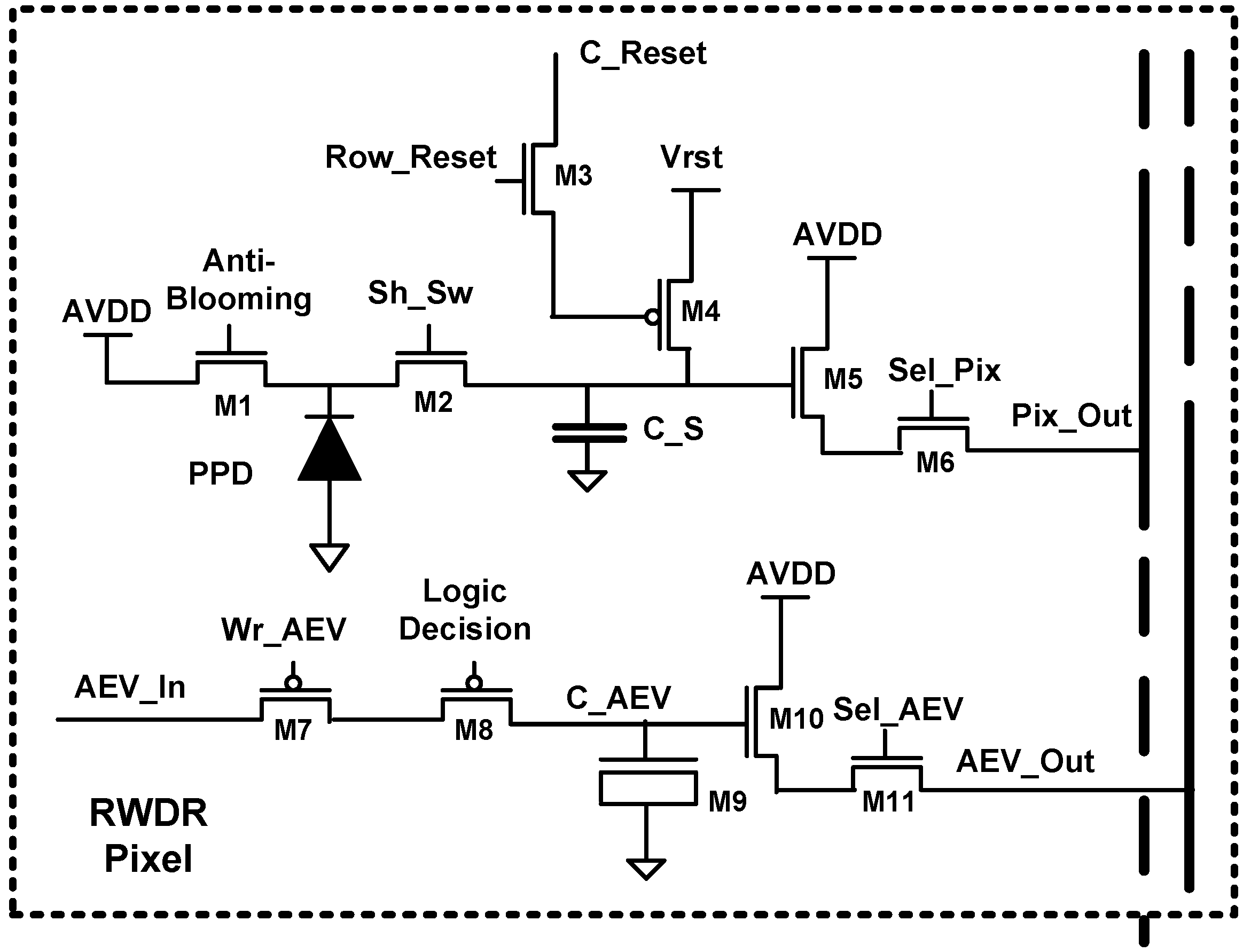
2.3. Phase 1: Assigning the Analog Encoding Voltage (AEV)

How are the values of AEV selected and paired with the corresponding EXP bits? The AEV values can be dispersed within the voltage domain in several ways: logarithmically or linearly (Figure 4). In this study we chose, for the sake of convenience, a linear quantization, according to which the all the AEV values are spaced at the same distance of 2ΔVmin. We also decided that the AEV corresponding to the highest light intensity would be represented by the lowest available voltage, since this simplifies all the subsequent conversions. The parameter ΔVmin is derived from the properties of the comparator that are to be employed for assigning the AEV values. The requirements for ΔVmin are intuitive and straightforward:
Jlpea 03 00027 i002
in which Vout_comparator, G, Voffset are the comparator’s output swing, gain, and offset, respectively.
Figure 4. Analog encoding voltage (AEV) concept: each dynamic range (DR) bit has its own Analog Encoding Voltage.
Jlpea 03 00027 g004
After the pixel array has been reset globally, Phase 1 begins. The pixels are exposed to light and accumulate the photo-generated charge. At certain predetermined time points, each pixel row is sampled nondestructively and spanned by a piecewise increasing ramp. In case the pixel signal intersects with the ramp, the comparator flips and the corresponding AEV is written into the in-pixel dynamic memory. Detailed considerations of the AEV assignment are provided in Appendix A.

2.4. Phase 2 Performing the Conditional Resets

Phase 2 performs the conditional resets to the pixel array. Since the base of the DR extension is 2, the integration times are ordered in exactly the same way as in our previous solutions [24], i.e., in geometric descending sequence:
Jlpea 03 00027 i003
Nonetheless, in the current solution, the pixel reset cycle can be reduced by a factor of 2 at least, since the number of operations before the conditional reset is halved. All that has to be done is to compare the individual AEV with the reference, which corresponds to the current reset cycle. This phase can be performed either in a traditional fashion, i.e., row by row scan, or instantly within the whole array. We will discuss in further detail two different designs implementing both of the options, namely TYPE I and TYPE II.

2.5. Phase 3: Coarse, Fine ADC & Readout

Phase 3 concludes the frame. At this stage, the analog pixel value (Mantissa) and the AEV are converted by the same comparators, which had been used in the two preceding phases. In fact, we performed a single slope ADC to obtain the digitized values of Mantissa and AEV (Figure 2). The conversion is performed row by row: first, the AEV is spanned with the “coarse” resolution, and then the pixel swing is spanned by the ramp with “fine” resolution. Of course, after the span, both the AEV and pixel capacitances are reset to their initial predetermined values.

2.6. TYPE I Pixel

For most applications the required dynamic range (DR) does not exceed 120 dBs, so the pixel structure can be straightforward. In our case, all we need is to accommodate the AEV and the pixel Mantissa on two separate capacitors and to add a readout chain and conditional access circuitry (Figure 5) to each of them. Since the pixel structure here is not complex and the DR extension is typical, this design is named TYPE I.
Figure 5. Schematic of TYPE I Pixel.
Jlpea 03 00027 g005
The functionality of the TYPE I pixel is implemented with 11 transistors only. They can be divided into two groups: the first processes the data received from the pinned photodiode (PPD) M1–M6; and the second is responsible for the AEV handling M7–M11.
The charge transfer from the PPD is bidirectional, similar to [25]. In this way, we can deliberately dump the generated charge to drain the photo-diode through M1 or we can transfer the charge for further processing to Cs through M2. We use a simple conditional reset scheme, implemented by M3 and M4 transistors, to implement the multiple resets algorithm. By activating the Row_Reset signal, the required pixel row is chosen and then, by means of the C_Reset signal, driven by the column-wise comparators, is conditionally reset to Vrst. Transistors M5, M6 form a traditional source follower to handle the CS readout [‎26].
AEV processing inside the pixel is very simple as well. The AEV value is fed to the pixel from the column-wise bus AEV_In. The write operation of the input AEV into the pixel dynamic memory is conditional and is implemented by using a trivial stacked scheme M7 and M8. By activating the Wr_AEV signal, a required row is accessed; while the Logic Decision signal, driven by column-wise comparators, enables the MOS capacitor CAEV to sample the AEV_In bus. It is important to note that aside from its simplicity, this stacked scheme also minimizes the possible leakage from the AEV capacitor, thus maintaining the data integrity till the readout. The readout of the AEV is performed through a separate source follower, implemented by M10 and 
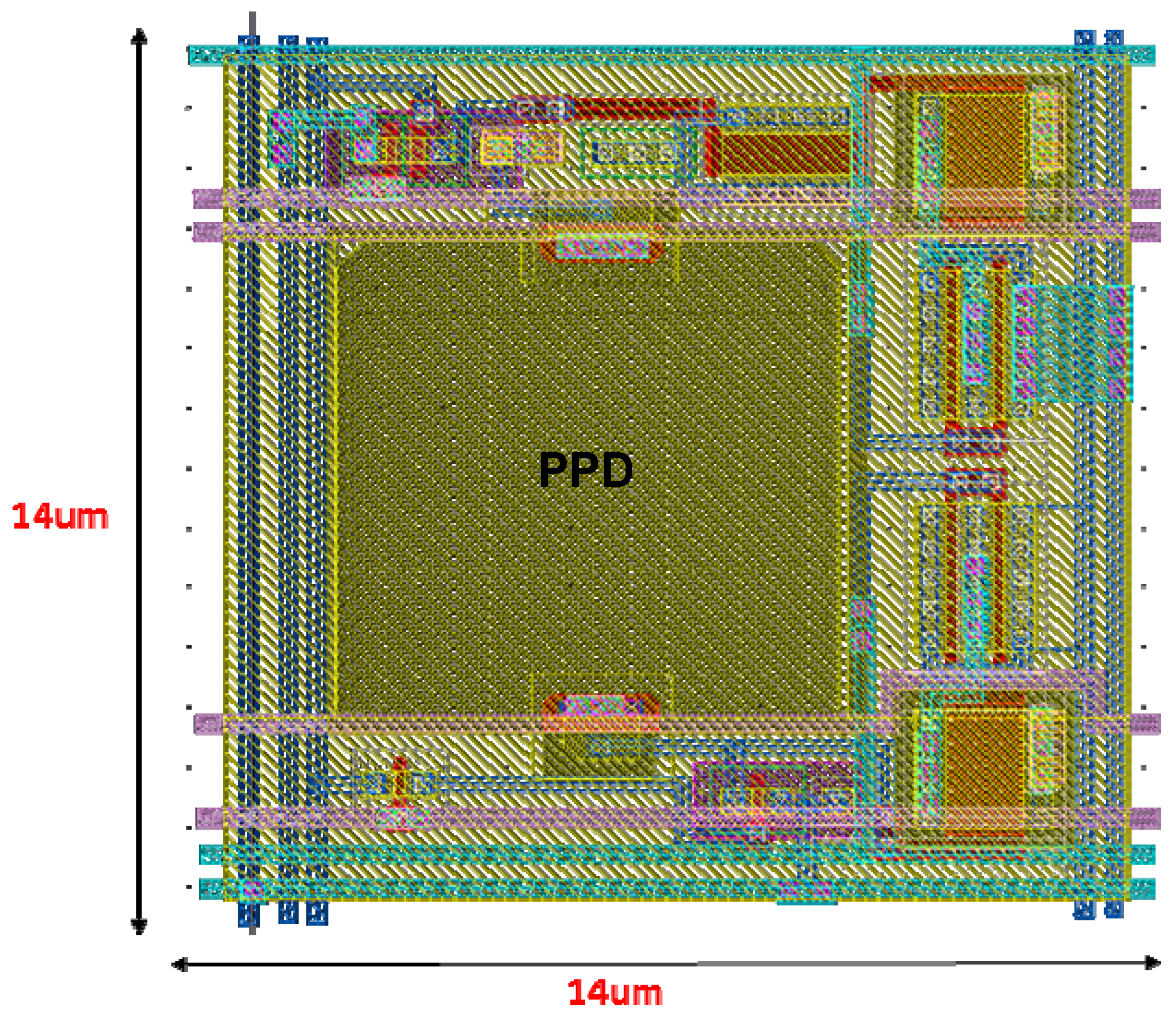
M11. This relatively simple pixel was implemented in layout using 0.18 µm CMOS technology, with 14 µm pitch and 40% fill factor (FF) (Figure 6).
Figure 6. Layout of TYPE I Pixel.
Jlpea 03 00027 g006
Figure 7. Phase 1 TYPE I pixel.
Jlpea 03 00027 g007
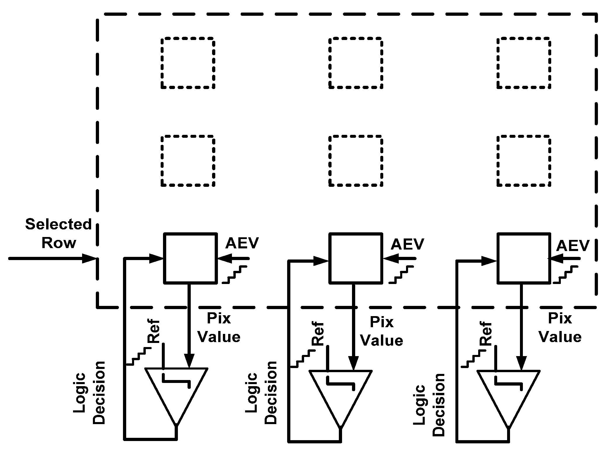
Figure 7 depicts Phase 1 for the TYPE I pixel. At each span, the pixel (Pix value) is being accessed by election of a specific row and is being compared to the reference signal Ref.
After Phase 1 is completed, Phase 2 begins. During this phase, each pixel integrates in accordance to the assigned AEV. After a certain integration slot (3) elapses, the AEV’s within each row are selected and compared with the Ref, which now reflects the reference values of integration times (Figure 8).
Figure 8. Phase 2 TYPE I pixel.
Jlpea 03 00027 g008
In our solution, the pixel is reset as long as its AEV is lower than the reference value.
In a TYPE I solution, the conditional resets are applied to each pixel row sequentially. The processing time, which takes to apply the conditional reset a single pixel row Trow_reset, is given by:
Jlpea 03 00027 i004
where TAEV_read and Tcompare are the time to sample the AEV and to decide to reset or not the referred pixel, respectively. Since two saturation checks cannot overlap each other, the time it takes to complete a single one sets the minimal integration time Tmin_TYPE I:
Jlpea 03 00027 i005
Given the minimal integration time, we can easily calculate the maximal possible DR extension factor (DRF) [8]. Through the performed simulations, we learned that the minimal integration time Tmin_TYPE I is 112 µs. Assuming the maximal integration time is 30 ms, we have obtained a DR extension factor equal to 256 (48 dB). The expected intrinsic DR i.e., before the extension is 60 dBs, consequently the total DR equals 108 dBs.
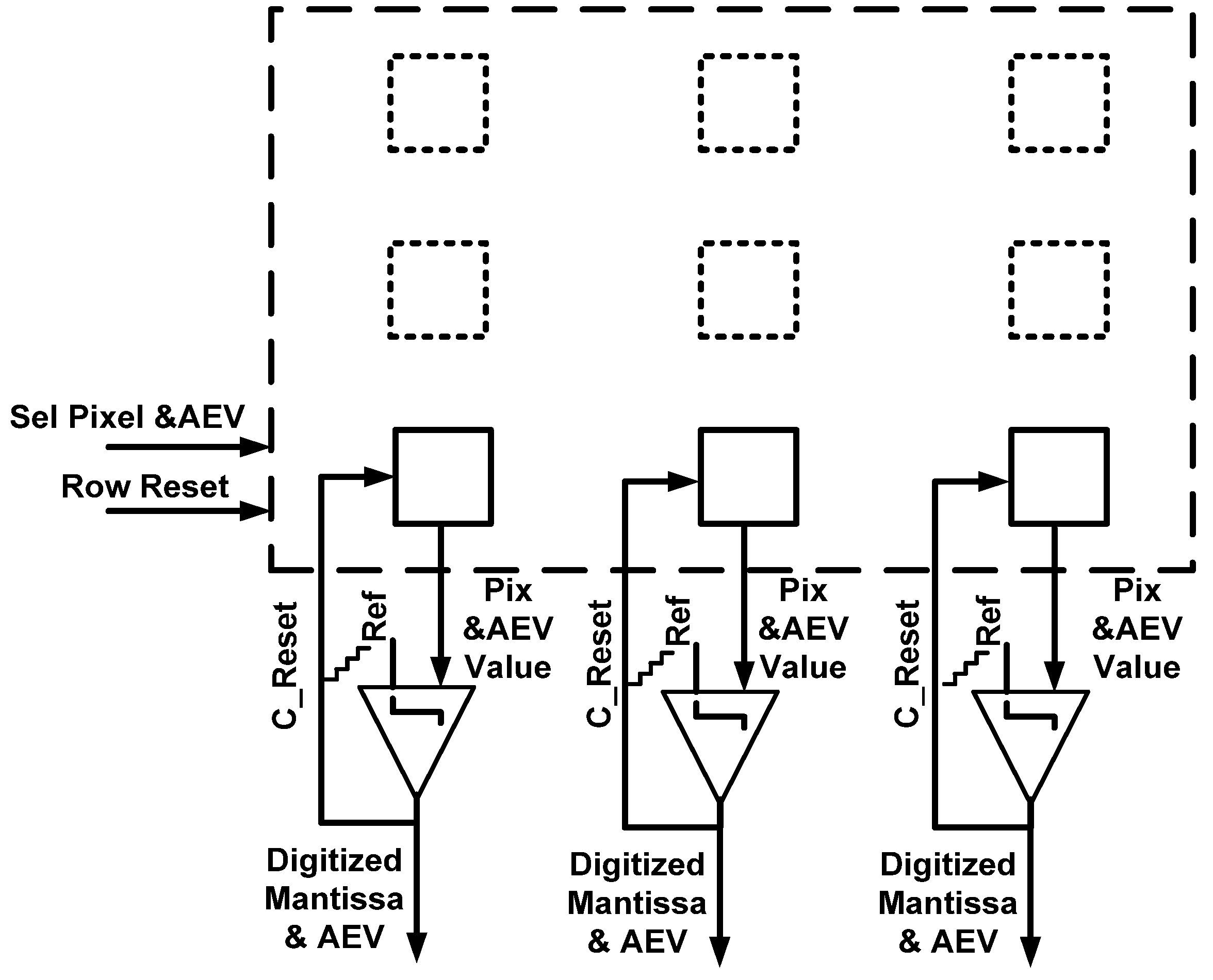
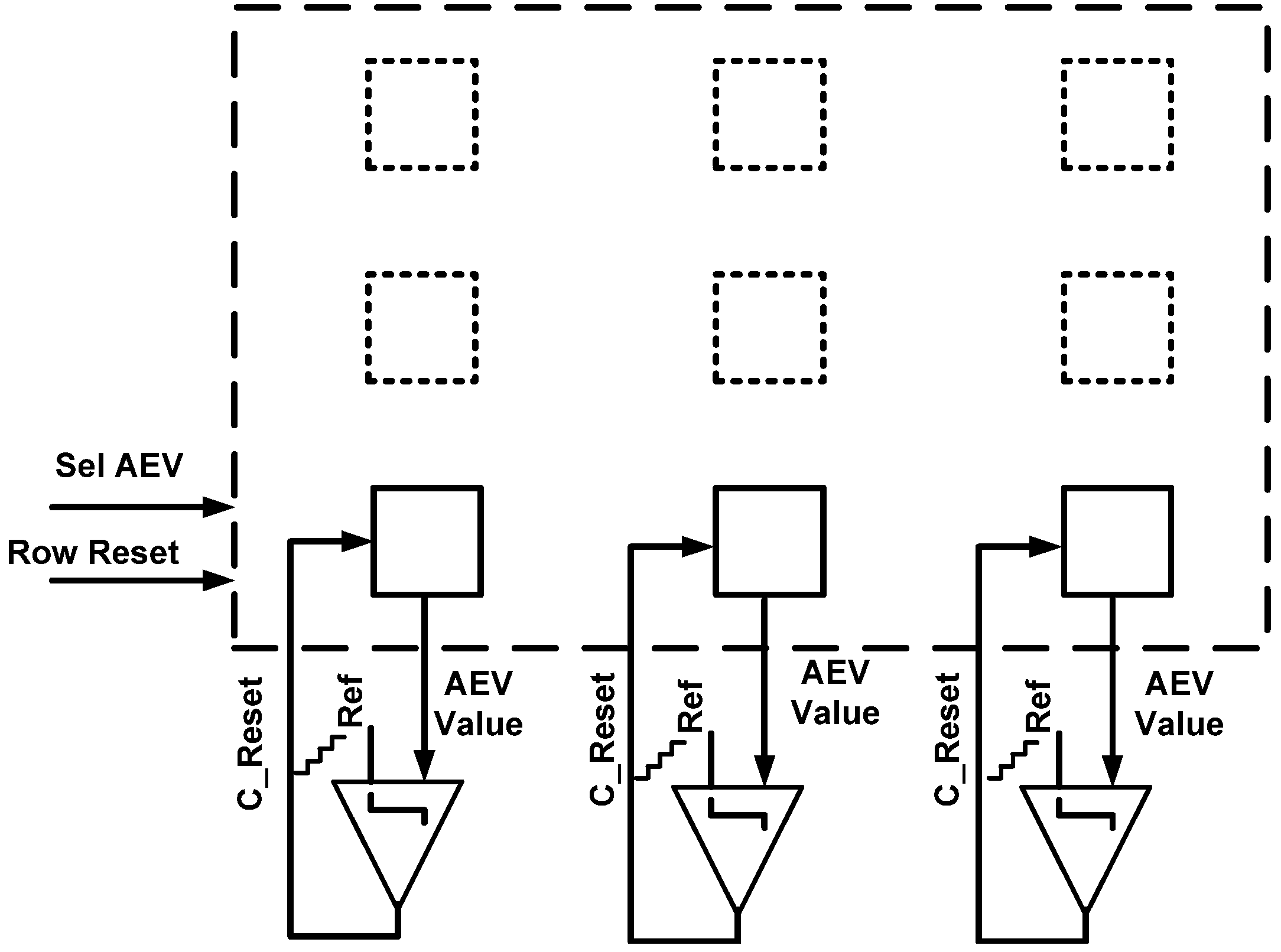
In the last phase of the frame (Figure 9), the accumulated data are accessed for the final ADC. By activating two separate select signals Sel_Pix and Sel_AEV, the pixel and the AEV, respectively, are digitized using the same comparators as in Phase 1
The TYPE I design was successfully tested in various post-layout simulations, which proved its feasibility. To reduce the length of this work, we present only the post-layout simulation results of the TYPE II design because it is much more complex. To conclude, CMOS sensor based upon the presented TYPE I pixel is capable of providing a DR of almost 5 decades operating at video frame rate and providing an image with a decent resolution.
Figure 9. Phase 3 TYPE I pixel.
Jlpea 03 00027 g009

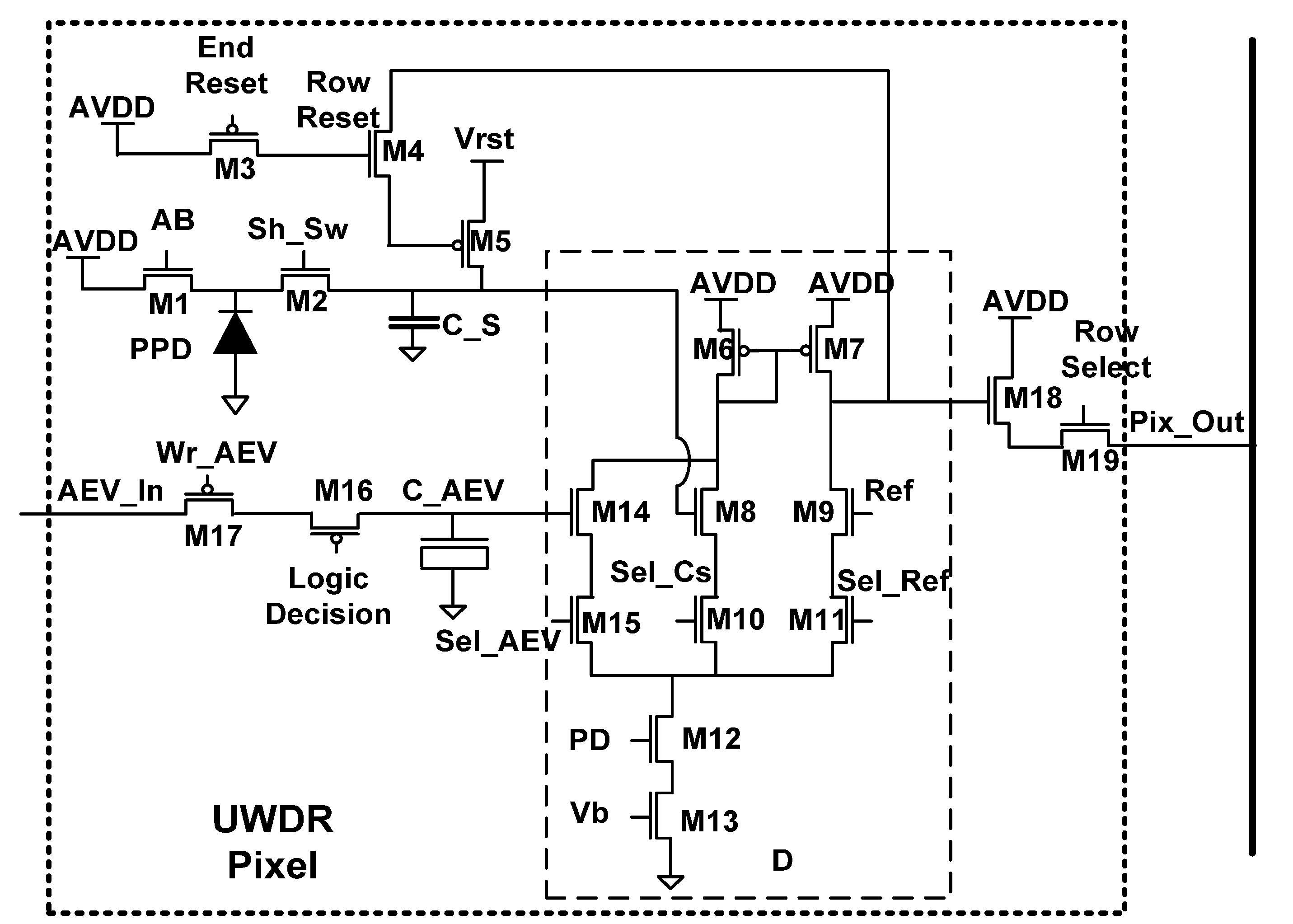
2.7. Ultra WDR (TYPE II) Pixel

The main difference between the Ultra WDR (TYPE II) pixel and the previous TYPE I solution lies in its accommodating a differential stage (D) within the pixel (Figure 10).
Figure 10. Schematic of TYPE II Pixel.
Jlpea 03 00027 g010
The inputs to this stage are: the pixel integration time represented by AEV (M14); the photo-generated signal (M8); and the global reference signal Ref (M9). These inputs are sampled from CAEV, CS, and Ref, respectively. By means of Sel_AEV (M15) or Sel_Cs (M10), the differential stage compares the AEV or the photo-generated signal, to the Ref. the transistor M11, controlled by Sel_Ref signal, was added to ensure an optimal matching within the differential amplifier. The bias point is controlled by an analog signal Vb (M13), which sets the current magnitude throughout the amplifier branches. To facilitate the power reduction, we inserted an additional transistor M12 in the series to the current source in order to shut down the entire stage, when no comparison is needed. The load of the D stage is implemented by two PMOS transistors: M6 and M7. The drain of the latter is connected to the drain of M4, forming a self-reset structure.
The self-reset feature of the D amplifier enables the application of the conditional reset operation during a saturation check simultaneously to every pixel within the array rather than row by row. At each saturation check, the Row Reset (M4) is raised globally, connecting the output of the D stage to the reset transistor M5. Obviously, when the amplifier’s output is low, the Cs capacitance is reset to Vrst, otherwise Cs remains without a change. To stop the reset cycle, regardless of the differential stage output, we use End Reset signal (M3), which forces AVDD on the gate of the reset transistor M5.
AEV assignments are done row by row as will be explained further. Before the assignment operation, the first AEV is asserted onto the AEV_In bus. Then, the signal Wr_AEV (M17) selects the appropriate pixels’ row. The Logic Decision signal (M16), which is driven by the column-wise common source amplifiers, enables the corresponding AEV to be sampled by the CAEV capacitor. The charge flow from the PPD is the same as in the TYPE I design throughout the whole frame.
At the end of the frame, both the AEV and the photo-generated charge are sampled nondestructively through the source follower (SF) (M18 and M19) and converted by column-wise amplifiers, as will be explained later.
Figure 11. Layout of the TYPE II Pixel.
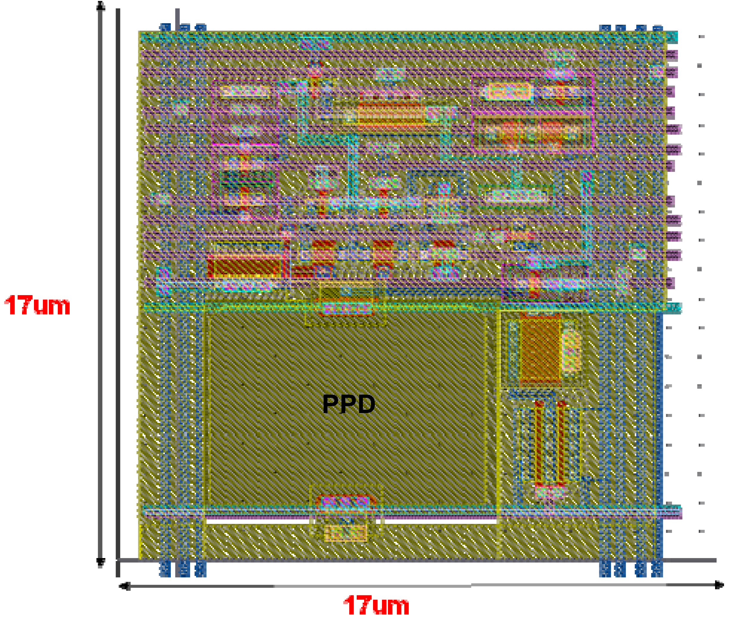
Jlpea 03 00027 g011
The TYPE II pixel was implemented in a 0.18 CMOS process (Figure 11). All the control signals were divided into two groups: 7 analog signals, and 10 logic signals. To reduce the coupling between the control lines, we used extensive orthogonal patterning, so that part of the signals was routed along the X axis, whereas another part was laid along the Y axis. The analog signals were implemented in Metal1 and placed along the Y axis to the left and to the right of the PPD. Such an arrangement reduced the coupling between the analog lines themselves and created a substantial separation from the rest logic signals, which were laid along the X axis. Moreover, all the signals, which were running horizontally, were implemented in Metal 3, which reduced the coupling between the pixel analog and logic lines even further. Due to the dense layout, we successfully implemented the described pixel with 17 µm pitch and 25% fill factor FF (Figure 11).
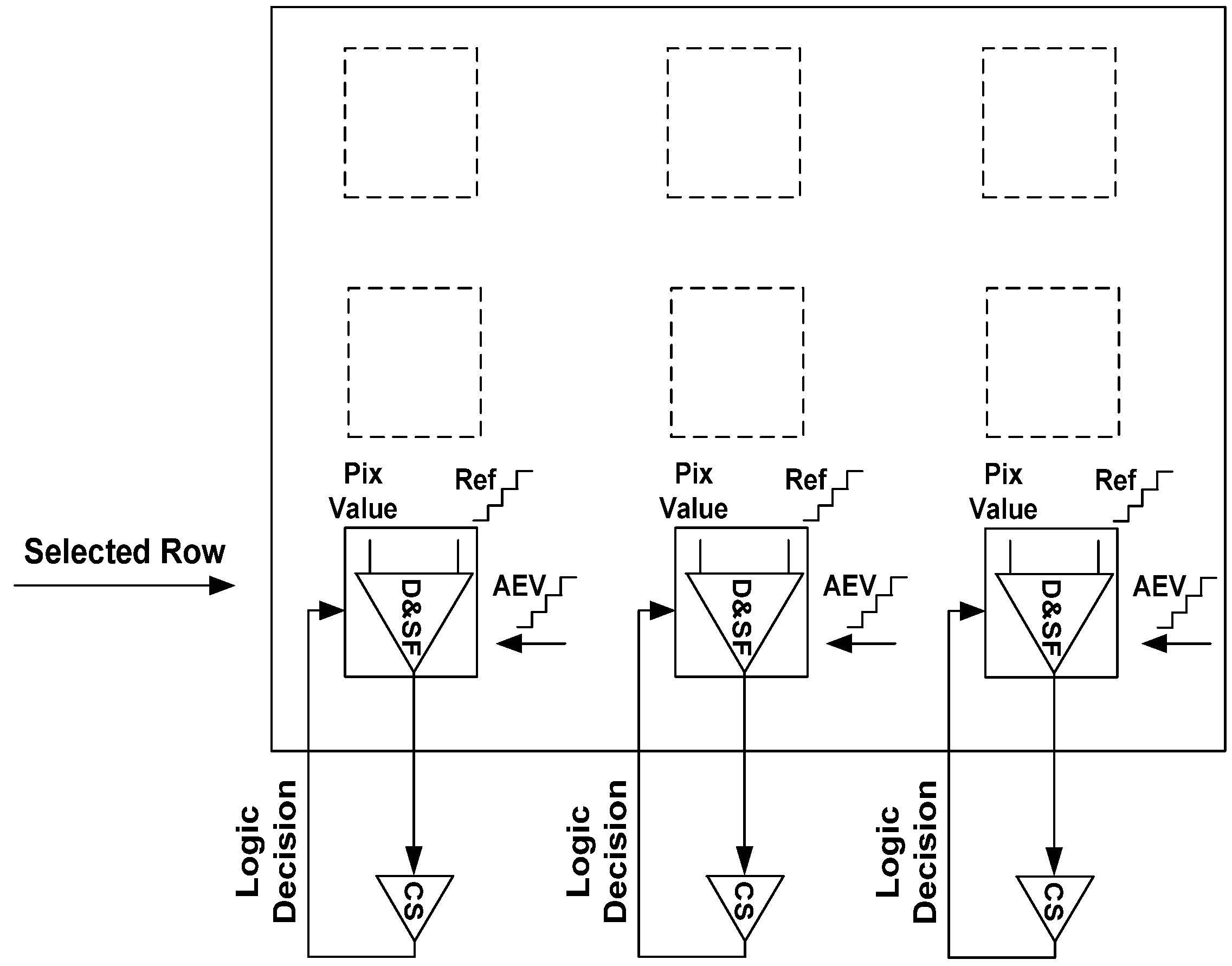
The three phases in the TYPE II solution are described in detail below. The AEV assignment that occurs in Phase 1 requires a high gain comparator. Since the gain of the in-pixel differential amplifier is not high enough, we added an external common source (CS) amplifier (Figure 12). In this way, we obtained the three stage high gain comparator: (1) D; (2) SF; (3) CS, respectively. The Pix Value is compared to Ref inside each pixel of the selected row. The final amplification is performed by CS, which drives the Logic Decision signal (Figure 12). This signal stamps the appropriate AEV value onto CAEV capacitance inside each pixel. 
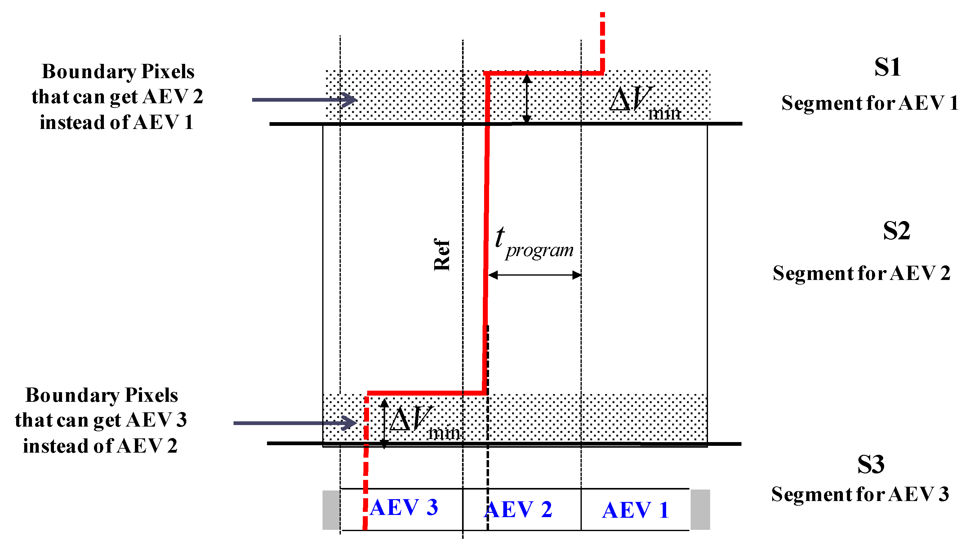
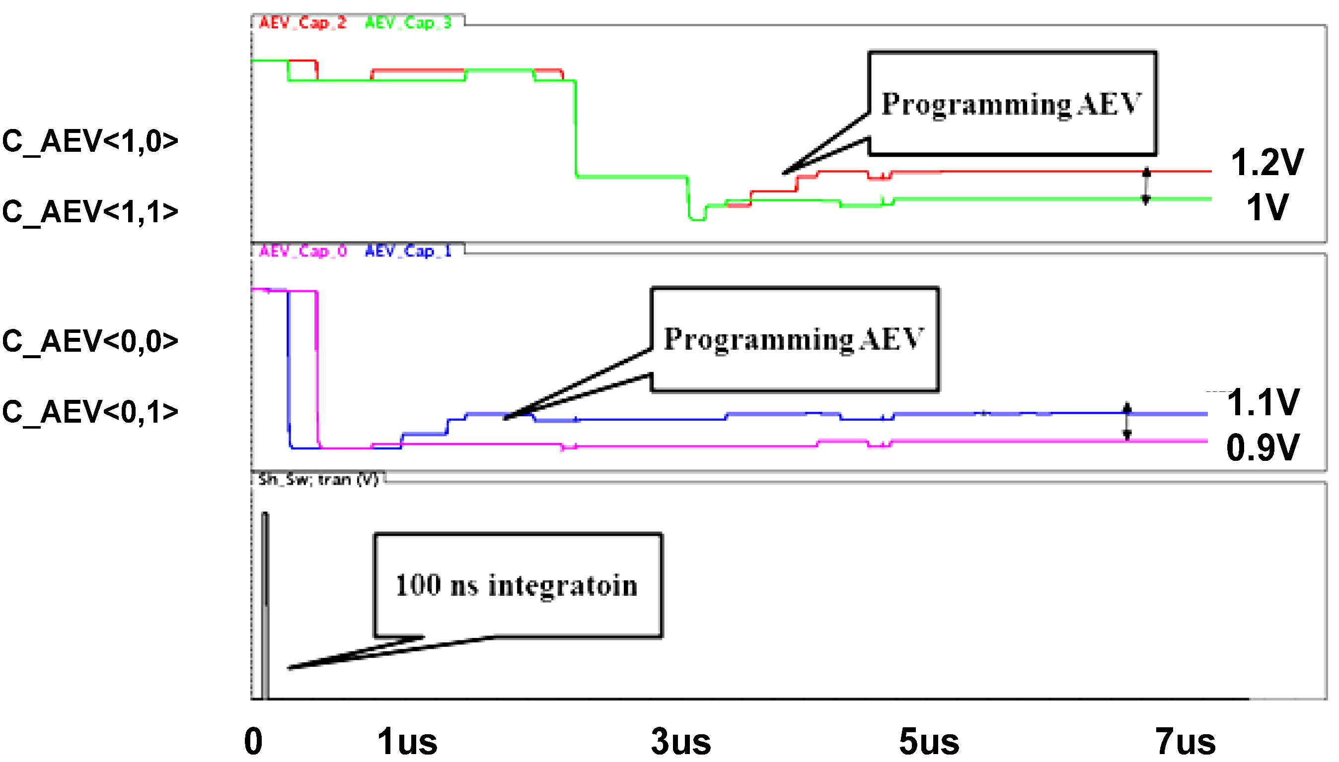
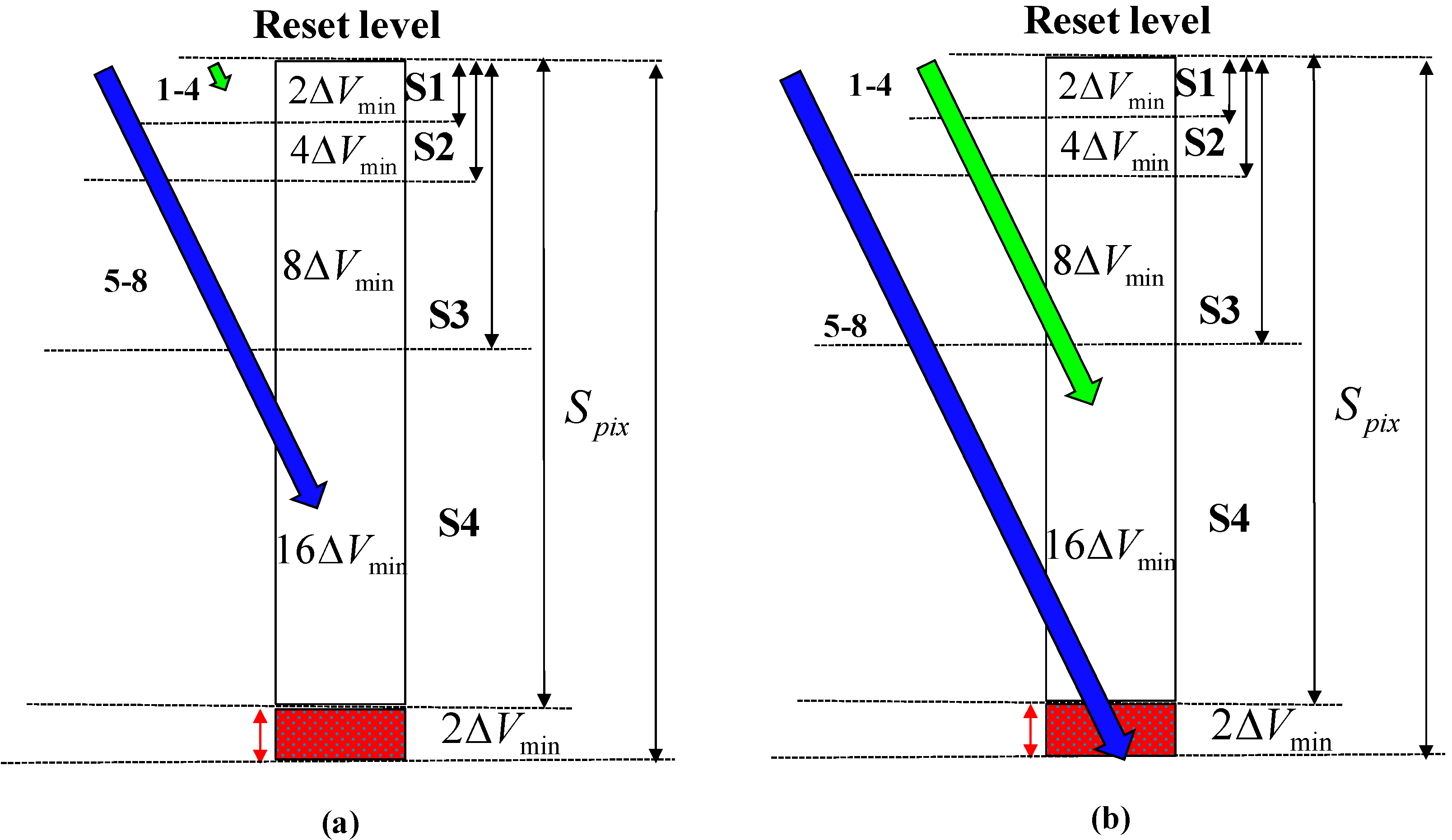
Figure 13 illustrates the flow of the AEV assignment to a pixel matrix of 2 × 2 at the first span. Each pixel within the matrix has its own coordinates: the first denotes the row and the second denotes the column. We performed the simulation as if each pixel within this matrix receives a different incoming signal. Therefore, we stimulated the pixels with different current sources, imitating different discharge rates. The AEV values were generated by a piecewise ascending ramp voltage ranging from 0.9 V up to 2.6 V, corresponding to 18 different values distanced by 0.1 V from each other. The first span occurs after 100ns. Then, the photo-generated charge is transferred to CS simultaneously within the whole matrix and is compared row by row with the reference, thus causing the corresponding AEV to be written onto CAEV capacitance (Figure 10). Capacitances CAEV<0,0> and CAEV<0,1>, found at the row <0>, are processed first, whereas row <1> capacitances are programmed after the completion of row <0> programming.
Figure 12. Phase 1 of TYPE II Pixel.
Jlpea 03 00027 g012
Figure 13. Post-Layout Simulation of Phase 1 of TYPE II Pixel.
Jlpea 03 00027 g013
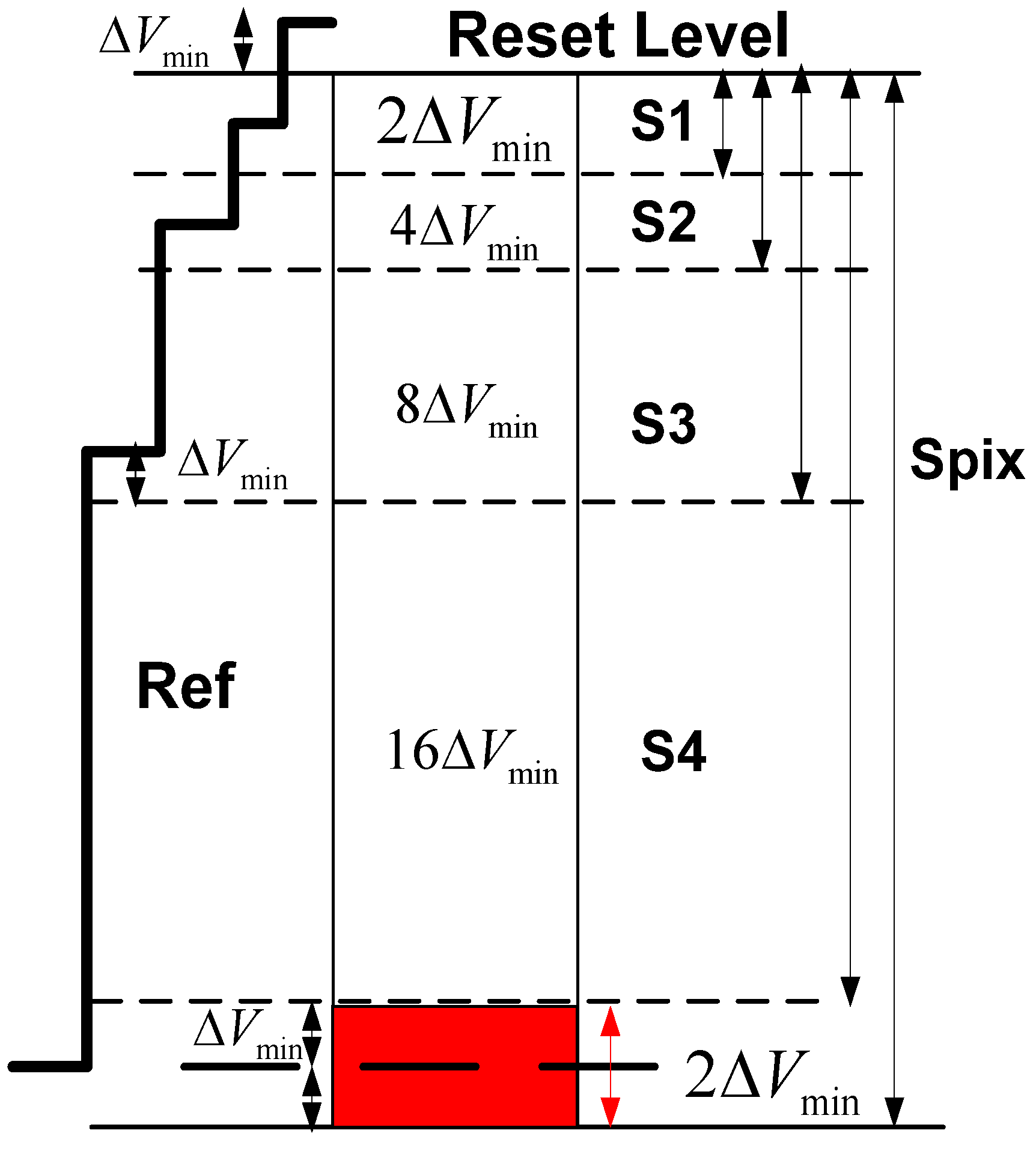
In the illustrated case, there are four different photo-generated signals, falling within four different segments; therefore every pixel is assigned a different AEV from 0.9 V to 1.2 V. The lowest AEV is assigned to the most illuminated pixel, i.e., to CAEV<0,1>, whereas the rest of the AEV’s: 1 V, 1.1 V, and 1.2 V are assigned to less illuminated pixels CAEV<1,1>, CAEV<0,0>, CAEV<1,0>, respectively. It is important to note that the adjacent AEV values differ from each other by 2∆Vmin, which is 0.1 V in this case, and this difference stays intact after the AEV’s were written to CAEV. In such a case, decoding the analog data at the end of the frame will be easy; otherwise the final pixel value will be erroneous due to a possible shift of the stored AEV values.
It is important to understand that the time of the first span is shorter than the minimal integration time, since, during all the spans, the available signal to be accumulated is lower than the pixel swing by 2ΔVmin. However, during the next phase the entire pixel swing is available, thus the real integration period will be somewhat higher. In the specific example we have discussed, the minimal integration time will be not 100 ns, but rather 112 ns.
Phase 2 in a TYPE II pixel is ultra-fast. Due to its self-reset ability, the reset decision inside each pixel is autonomously fed from the differential stage through M4 to the gate of M5 (Figure 10). Consequently, each pixel is reset independently upon the comparison of its own AEV with the global reference Ref (Figure 14). Therefore, the minimal integration time for this design is:
Jlpea 03 00027 i006
Figure 14. Phase 2 of TYPE II Pixel.
Jlpea 03 00027 g014
Equation (6), which describes the minimal pixel conditional reset time, sets the minimal integration time and, as such, defines the available DR extension. In this case, the minimal integration times can be set as low as 112ns, which enables the DR to be extended by over five decades.
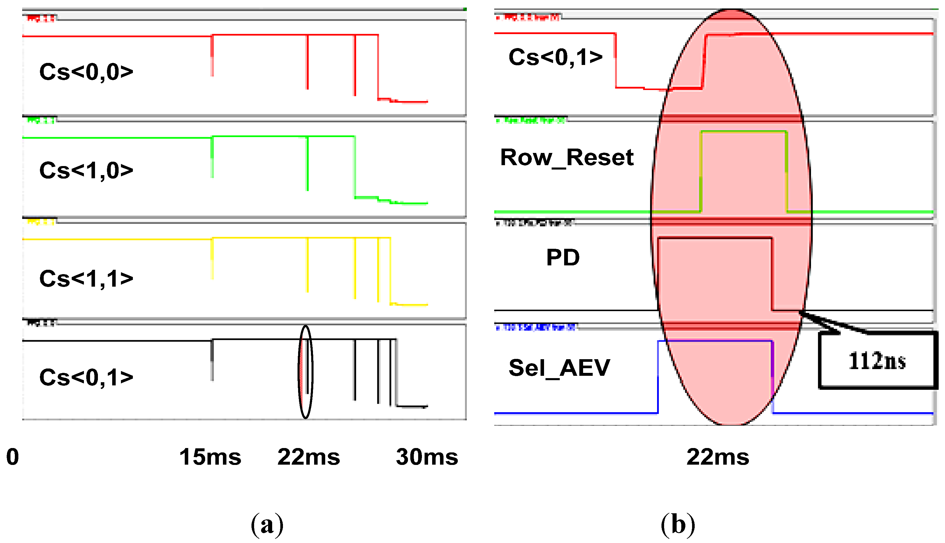
Figure 15a,b illustrates the flow of Phase 2 on a matrix of 2 × 2 pixels. There are four different illuminated pixels, each with its own AEV in Phase 1. At Phase 2, every pixel is reset in accordance with its AEV (Figure 15a). The bottom pixel, CS<0,1>, has the lowest AEV and therefore it is reset for five times; whereas the pixel CS<1,0>with the highest AEV is reset only twice. A close–up of the typical reset sequence is presented in Figure 15b. First, the differential stage inside the pixel is activated by raising the PD signal; then, the AEV is compared to a reference by raising Sel_AEV. After this, the bias point of the amplifier stabilizes, the Row Reset signal is activated, which enables the decision to reach the reset transistor. In the specific case we have presented, the reset decision is positive and therefore the capacitance Cs<0,1> is charged up. The whole sequence lasts for 112 ns; thus, by assuming a typical frame time of 30 ms, we obtain DR extension of 109 dB [‎8]. Adding to this the intrinsic DR of 60 dBs (10 bits), we obtain overall DR of 170 dB approximately.
Figure 15. Post-Layout simulation of: (a) 4 different pixel signals during Phase 1; (b) a close up of a single self-reset cycle.
Jlpea 03 00027 g015
The final A/D conversion occurs at Phase 3. We use the same comparator configuration as depicted in Figure 12 to perform a single slope conversion to a photo-generated signal (Mantissa) and to an AEV. Figure 16 depicts the process of A/D conversion to the stored AEV and the pixel Mantissa. First, the pixel AEV is converted using a ramp with reduced (“coarse”) resolution. It can easily be observed that the Ref signal spans the AEV domain in a reduced number of steps, which corresponds to the “coarse” conversion; whereas, the pixel Mantissa is spanned by the reference with a much higher (“fine”) resolution. As a matter of fact, after the Mantissa is converted, the capacitance CS storing it is being reset for the next frame. The capacitance holding the AEV is not necessary to be reset, since it will be assigned the new AEV in Phase 1 of the subsequent frame in any case.
Figure 16. Post-Layout Simulation of Phase 3 of TYPE II pixel.
Jlpea 03 00027 g016
In conclusion, the relatively complex structure of the TYPE II pixel has enabled a very large DR extension and has substantially simplified the second and the third phases of the proposed algorithm. Figure 15, Figure 16 prove the feasibility of the TYPE II design and indicate that sensor based upon a TYPE II pixel can be successfully implemented in a silicon process.

2.8. A Power Profile of TYPE I and TYPE II Designs

Another important factor is the examination of the power performance of the TYPE I and TYPE II designs, since, if they were power hungry, it would be pointless using them. We made both of the designs optimized for low power using the following methods: the two stacked transistors scheme, and multiple power supplies. The result was that the leakage within the pixels was successfully minimized, and the power supplies could be lowered easily without degrading the anticipated sensor's performance.
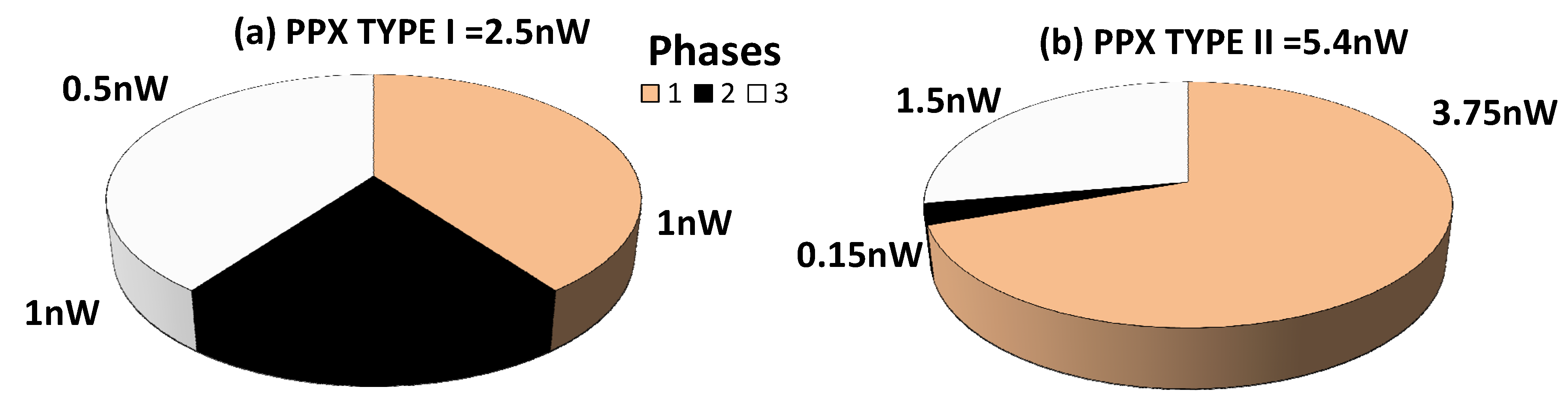
In analyzing the TYPE I power per pixel (PPX), we have concluded that most of the power is consumed during the AEV assignment (Phase 1) and the A/D conversion (Phase 3), because these two operations require activating the comparators for a longer period of time than in Phase 2 (Figure 17a).
In TYPE II, the relative power contribution of Phase 2 is also the lowest, in comparison with the two other phases, as its overall effective duration is the shortest one (Figure 17b). Most of the power is consumed during Phase 1, which contains an increased number of spans and, thereby, in aggregate, lasts longer than Phase 3. Phase 3’s contribution to PPX, is almost the same as in the TYPE I case due to similar flow of the data conversion.
Based on these simulations, we have concluded that the two presented designs consume power of 2.5 nW and 5.4 nW, respectively. Taking into account the anticipated extraordinary DR extension they provide, we have found that the power budget is low and definitely appropriate to the state-of-the art CMOS image sensors [25].
Figure 17. Power per Pixel Distribution of TYPE I and TYPE II Designs. (a) PPX TYPE I = 2.5 nW; (b) PPX TYPE I = 5.4 nW.
Jlpea 03 00027 g017
To summarize the anticipated performance of the proposed designs, we provide Table 1, where different state-of-the art WDR solutions are compared with respect to several key attributes such as fabrication technology, WDR technique (WDR T.), pixel size, fill factor (FF), DR, SNR, power per pixel (PPX), and frame rate (FR).
Table 1. Comparison between state-of-the art WDR image sensors.
Parameter[11][5][12][14][21]TYPE ITYPE II
Technology0.18 µm0.09 µm0.18 µm0.35 µm0.18 µm0.18 µm0.18 µm
WDR T.Well Cap.AdjustmentWell Cap.AdjustmentFrequencyTFSMultiple Capt.Multiple ResetsMultiple Resets
Pixel Size3 µm × 3 µm5.86 µm × 5.86 µm23 µm × 23 µm81.5 µm × 76.5 µm5.6 µm × 5.6 µm14 µm × 14 µm17 µm × 17 µm
FF--25%2%45%40%25%
DR100 dB83 dB130 dB100 dB99d B108 dB170 dB
SNR48 dB*48 dB *---48 dB *48 dB *
PPX-400 nW **250 nW≤6.4 µW **10 nW **2.5 nW5.4 nW
FR-30--153333
(*): The SNR was assessed based upon the well capacity of the photo-diode; (**): The PPX was calculated by normalization of total power by the number of pixels within the array.
From Table 1, we can understand that the pixel sizes of pixels presented in our work are mediocre. They are substantially larger than those associated with well capacity adjustment and multiple captures, but much smaller than frequency and TFS based sensors. Important to note that both of our designs maintain a decent FF relatively other listed solutions due to area effective layout. The DR of proposed herein designs emphasizes the extraordinary ability of multiple resets algorithm to extend the pixel dynamic range. TYPE I provides remarkable DR, whilst TYPE II brings it to extreme values. Moreover, such DR is obtained, maintaining excellent SNR (see Appendix B). Not less important to note that both of proposed designs operate at video frame rate and present the best power performance.

3. A Comparative Analysis of Multiple Captures & Multiple Resets Algorithms

When a new WDR solution is proposed, it is always interesting to compare it to the existing ones and to realize the added value the new solution contributes. In the present discussion, we perform a comparison between the two proposed solutions to the following algorithms: the multiple captures [15] and the former multiple resets solutions [24]. We chose to compare the number of operations needed to obtain a single digitized WDR pixel value; because, in our opinion, the most significant contribution of TYPE I and TYPE II solutions is their effectiveness and their ability to substantially reduce the processing time.
First, the multiple captures algorithm must be considered. In this solution, the pixel integrates for several periods of time, regardless of the intensity of the incoming light. After each integration, the intermediate pixel value is synthesized out of both the newly generated and previously stored samples, respectively. At this stage we assume that all the captures are performed in a rolling shutter mode to comply with the minimal memory requirements for this solution. In case multiple captures are performed in a global shutter mode, the memory requirements will be much higher. For a rolling shutter operation mode, the number of memory bits for each pixel equals its digital resolution: Nresolution. The total number of operations that are required to obtain a final digitized result for a single pixel after Ncaptures exposures is:
Jlpea 03 00027 i007
where 1convert, 1read, and 1write stand for ADC, memory read, and write cycles, respectively. Please note, that in this case there are two captures only: the memory actually becomes a single row register where the first sample is kept, in order to be compared with the second.
On the other hand, both the previous and newly proposed multiple resets solutions are applied on a global shutter sensor to obtain the maximal possible number of operations. According to the snapshot mode, the number of memory bits for a single pixel equals RepEXP, which is the representation of the exponent bits NEXP. Obviously, in case of linear representation, RepEXP equals NEXP. If logarithmic representation is applied, the RepEXP is reduced to log2NEXP + 1 [27]. For example, if there are 6 exponent bits, then in the first case, RepEXP is 6, whereas in the second it is 4. The overall number of operations in previous solutions is:
Jlpea 03 00027 i008
The first term in (8), relates to the sequential generation of DR bits, which consists of memory read, pixel conversion by the comparator, and memory write cycles. The second term relates to the digital readout of the memory contents, and the last term denotes the A/D conversion of the pixel Mantissa at the end of the frame.
In the newly presented TYPE I and TYPE II solutions, the total number of operations coincides with:
Jlpea 03 00027 i009
The term l stands for the number of spans performed during Phase 1; NEXP is for Phase 2, and the last term of 2 denotes the number of conversions during Phase 3.
Next, we will demonstrate the meaning of Equations (7–9) by substituting the possible values for each parameter. We have presented the results in Table 2, where each row is allocated for a different Ncaptures and NEXP.
For the previous solutions of multiple resets, we chose the logarithmical representation as in [27], because it minimizes the required external memory size. We also have assumed that the number of the exponent bits NEXP equals the number of captures: Ncaptures. This assumption not only simplifies the calculations, but it also ensures that the SNR dips, which exist throughout the extended DR in all of the solutions, are equal.
The advantage of the multiple captures algorithm is that most of it is implemented in a digital domain and the pixel structure is rather simple. The clear disadvantage is that this solution requires an extensive processing to obtain the final result. From Equation (7), it is shown that the number of operations increases linearly with the number of captures. This fact is clearly demonstrated by Table 2, where the multiple captures solution obviously possesses the highest number of operations per pixel. It is possible, though, to limit the number of captures to two or three; however this will cause large SNR dips at the boundary light intensities [8]. Circumventing these SNR artifacts by adding more integration slots will certainly slow the sensor operation speed. Consequently, the multiple captures algorithm is best suited to photograph slow changing scenes with a very high spatial resolution.
Table 2. The Comparison of a number of operations for “Multiple Captures”, “Multiple Resets Previous”, and “Multiple Resets New” algorithms.
NEXP = Ncaptures
Ncaptures = NEXPMultiple Captures [15]Multiple Resets Previous [27]Multiple Resets New (This Work)
22195
342136
463167
61052310
183576125
In the multiple resets algorithm, although the pixel structure and the pixel control are more complex than in the first case, the overall processing is much faster, since the pixel adjusts the integration time autonomously during the frame. Thus, there is no need for an extensive post-integration processing—only to combine the data of the Mantissa and the EXP bits. From Table 2, we realize that even the previous configurations of multiple resets have a reduced number of operations, relative to the multiple captures algorithm. The intuitive explanation of this is found within a sequential processing of the pixel information, which allows reading only the last produced bit from the memory before generating the subsequent one. The logarithmical representation of the EXP bits, used in the previous designs, decreases the operations number even further. Therefore, the previous solutions of multiple resets were perfectly suited to capture fast changing WDR scenes with a decent resolution.
The two solutions, proposed within the current study, bring the number of operations to its minimum, since they completely eliminate the operations related to a digital memory unit. This feature enables the proposed solutions to be the fastest among the three, which have been analyzed in this discussion. The clear disadvantage of the pixel using AEV is a relatively complex analog signal processing inside each pixel, which is especially pronounced in TYPE II design. Therefore, the newly proposed solutions can be candidates for implementation for capturing a very fast changing scene with wide or ultra-wide dynamic range.

4. Summary

We have presented two designs: TYPE I and TYPE II featuring the “ranging” and the AEV concepts. We have shown that it is possible to perform effective encoding of the DR bits using analog voltage, which can be easily stored within the pixel and processed further through the readout chain. Moreover, we have condensed the AEV assignment to a single phase in a process called “ranging”, which has led to another improvement: a substantial simplification of the conditional reset. In the past, each cycle consisted of three or even more different operations; now the number of operations has been nearly halved. The AEV solution has also granted a possibility to save chip area due to reuse of high gain comparators as a main block in a single slope ADC. The post-layout simulations and power calculations included in our study have shown that both the TYPE I and the TYPE II designs are feasible and can be successfully implemented in a CMOS process. The presented designs have reached a remarkable DR of up to 170 dB, while only consuming power of up to 5.4 nW. A further comparison between this work and the multiple captures and the former multiple resets solutions has clearly proven that the AEV concept effectively reduces the number of operations required to produce a pixel value and, as such, can be considered as a key to design a fast, low-power and ultra WDR CMOS sensor.

Appendix A

Division of the Pixel Swing to Segments

Since our algorithm is based upon integration times ordered in geometrical progression, we divide the pixel swing Spix into geometrically ordered segments as well: S1, S2,…, Sn as depicted in Figure 18.
During the frame, the pixel discharges from the Reset level towards the noise floor. The Reset level and the lower bound of pixel signal define the pixel swing Spix. The first segment S1 equals 2ΔVmin. Consequently, the subsequent segments will be equal to 4ΔVmin, 8ΔVmin, and so on, till the last segment Sn, (Figure 18). In the general form, the values of these segments are given by:
Jlpea 03 00027 i010
It is important to note that the last segment Sn, is distanced from the pixel swing Spix by 2ΔVmin. This means that signals exceeding Sn will not be converted. The purpose of this restriction will be explained later on.
That the number of AEV values that can be assigned in a single span equals the number of segments, which are given from (10) can be easily understood. For example, as shown in (Figure 18) if the pixel Sn equals 16ΔVmin, there will be four different segments; thus, four values of AEVs can be assigned during a single conversion.
The ramp signal Ref spans the pixel signal. This signal has to comply with the following requirements: (1) the signals that reach the lower bound of Spix will not be converted; and (2) signals reaching the edge of the last segment, S4 in this case, will be converted. In this way, the ramp starts on its way in the middle of the restricted region marked in red (Figure 19).
Figure 18. Division of the Pixel Swing to Segments.
Jlpea 03 00027 g018
Figure 19. Conversion of a pixel swing composed out of four segments.
Jlpea 03 00027 g019
From there, it climbs in geometrically decreasing steps, gradually covering all the pixel segments. To insure that all the segments are duly covered, the ramp Ref surpasses each one by ΔVmin. An additional positive consequence of such ramp configuration is that the minimal SNR during each conversion is set by ΔVmin (see Appendix B).
Special attention needs to be paid to the synchronization between the change of AEV and the ramp steps (Figure 20). Please note that AEV 2 becomes valid before the Ref continues to climb and it stays constant for the tprogram interval, during which the AEV 2 value is being written onto the CAEV.
Figure 20. AEV change in correlation with the comparator reference.
Jlpea 03 00027 g020
Another essential aspect is the assignment of the AEV values to the pixels, the signals of which lie at the boundaries of the adjacent segments. Such Boundary Pixels can receive the AEV value corresponding to the previous segment. For example, the ramp Ref finalizes spanning the pixel signals that should receive AEV 2 within the adjacent S1 segment. In such a situation, some pixels, found at the lower boundary of a S1 segment can mistakenly receive AEV 2 instead of AEV 1. As a result, the pixels’ saturation is prevented, but this is at the expense of the reduction of half of their effective integration time, which leads to a SNR drop of 6 dBs.
Up to this point, we have explained the aspects of a single pixel span, but what happens if we were to perform additional spans to complete the desired number of EXP bits NEXP? Then, the number of spans l is increased to (11). For example, if we suppose there are 18 bits to be encoded into 18 AEV values and in each span 4 bits are encoded, then 5 scans are needed to complete Phase 1.
Jlpea 03 00027 i011
where n is the number of segments. Since there might be several spans, how are we to ensure that AEVs, which were assigned in the preceding spans, are not overridden in the subsequent ones? The answer is to distance the last segment by 2ΔVmin from the pixel lower boundary. If we look for the reason the AEV’s were not overridden, we learn that there are two spans necessary to encode eight different light intensities “1–8” (Figure 21a,b). After the first span, the four most significant intensities “5–8” are covered and assigned their AEV’s (Figure 21a). The weaker four intensities (“1–4”) are assigned AEV’s, which are not correct and therefore should be overwritten in the upcoming second span. During the second span, all the pixels will be addressed once again, regardless if they have already received their AEV’s or not. The second span is distanced from the first, so that the signal generated by “5–8” exceeds the last segment by 2ΔVmin. Therefore, these pixels do not receive new AEV’s. On the other hand, “1–4” intensities generate signals, which now fall within the different segments and thereby are assigned the corresponding AEV’s (Figure 21b). Hence, by the reduction of the possible conversion range, we can differentiate between the already encoded pixels and those which should be encoded in the future spans.
Figure 21. Distribution of the different light intensities by segments (a) first span; (b) second span.
Jlpea 03 00027 g021
All the spans are spread non-uniformly in time. The occurrence of each span tk is set upon the most significant EXP bit that can be encoded in the k-th span:
Jlpea 03 00027 i012
where Mk is the MSB that can be encoded in the k-th span. For example, if there are 18 EXP bits to be encoded during 5 spans, then M1 = 18; M2 = 14; M3 = 10; M4 = 6; M5 = 2, respectively. Furthermore, assuming that Spix = 1 V; 2ΔVmin = 0.112 V; Tint = 30 ms, the span times t1 till t5 are: 100 ns; 1.65 µs, 26.4 µs, 422 µs, and 6.75 ms, respectively.

Appendix B

SNR Considerations

SNR is one of the key properties of every sensor. Every designer must be aware how much noise each specific circuitry architecture generates. Herein, we discuss three noise sources shot noise, flicker noise, and the thermal noise. We consider the noise of the two types of the sensors separately. The performed analysis shows that in poorly illuminated scenes, the thermal noise governs the noise floor for both of the sensors, whereas the shot noise of photo-diode sets the noise limit in highly illuminated scenes. We refer to noise induced to AEV capacitance as well, and show that our design considerations provide an excellent signal to noise ratio of the stored data throughout the whole frame.

TYPE I

We assume, for our convenience that all noise sources are uncorrelated, therefore we can write the overall SNR as:
Jlpea 03 00027 i013
where Vn_KTC, Vn_shot, Vn_read are the voltage variances of the thermally generated KTC noise, shot noise, and read noise, respectively. iph denotes the photo-generated current and tint denotes the time it is integrated within the photo-diode.
The noise analysis for this sensor is straightforward, due to its conventional structure. At the beginning of the frame, the in-pixel sense capacitance CS (Figure 5) is being reset, which causes well-known KTC noise. Since it is “hard reset” [‎28], performed through PMOS, the overall inflicted noise equals:
Jlpea 03 00027 i014
where kB and T are the Boltzman’s constant and junction temperature in degrees of Kelvin, respectively. According to our assessments, the resulted noise equals to 643 µV. Note, that since at the end of the frame, we do not need to convert the reset signal as in other conventional designs, this noise is not doubled. In case, there are multiple resets applied, this noise contribution grows by the square root of the reset times.
Shot noise within the photodiode is inflicted by both the dark current idc and the incoming optical signal iph [28]. The overall noise contribution is given by:
Jlpea 03 00027 i015
In case the accumulated charge is maximal, i.e., it equals the pixel swing Spix, we get the following noise:
Jlpea 03 00027 i016
According to our assessments this amount of noise can reach 4 mV. In such a case the maximal SNR according to (16) equals 48 dB.
The readout noise in this sensor is mainly generated by the in-pixel source follower amplifiers, through which the readouts of AEV and the pixel are performed. It is easy to show that the noise source follower amplifier generates [29] is given by:
Jlpea 03 00027 i017
where CPix_Out, CAEV_Out, are the sample capacitances for pixel and the AEV readout, respectively. One should note that since the gain of source follower never exceeds unity, the load capacitances should be large enough to reduce the readout noise to desirable level. In our case, the sample capacitances were designed to be no less than 100 fF, which bounded the readout noise to 200 µV, approximately.
It must be noted that there are additional noise sources within the source follower amplifier such as: flicker and telegraph noise [28]. The power of these noise sources is strongly depends on the process quality. With the recent fabrication technology advances, the total contribution of theses noise sources has been reduced to couple of electrons rms, which in our case equal to couple of tens micro-volts.
Additional noise sources, which have to be taken into consideration during the readout, is the thermal noise generated by the column-wise high gain comparator (Figure 7). The comparator consists of two stages: differential and common source. It is easy to show that the input referred thermal noise voltage variance is given by [29]:
Jlpea 03 00027 i018
where CCS_in is the common source input capacitance and GDiff is the differential stage gain. Correspondingly, the noise generated by the common source is:
Jlpea 03 00027 i019
Substituting the corresponding values into (18), (19), we assessed that the input referred noise coming from the comparator is 55 µV, which is substantially lower than the one induced by the source follower.
The in-pixel dynamic capacitance storing AEV value also accommodates a certain amount of noise. Apparently, it is the KTC noise, which is injected onto CAEV (Figure 5) the moment the Logic Decision signal disconnects it from the AEV_In bus. The amount of noise can be calculated by (14) by substituting CAEV value into that formula. Since CAEV is almost the same as CS the noise equals 643 µV as well. Taking into account that the minimal difference between the AEV value and the reference signal Ref (Figure 19) is ΔVmin, we get the following minimal SNR:
Jlpea 03 00027 i020
For example, if CAEV is 10 fF and ΔVmin is 50 mV, we can observe that the minimal SNR is 37 dB, which is enough for obtaining 4–5 bits resolution during each span.
To conclude, TYPE I sensor reaches 48 dB SNR, when exposed to high light intensities. The dominant noise at low light is the KTC, whereas at high end it is the shot noise, which limits the sensor performance.

TYPE II

The SNR in this sensor is also given by (13). The first two terms of noise, namely Vn_KTC, Vn_shot, are similar to the TYPE I sensor. The readout noise, however, is much lower due to accommodation of the differential stage inside the pixel. In this configuration, the noise contributions of source follower, common source become reduced by the gain of the in-pixel differential stage. Thus, employing Equations (17)–(19), we can assess that the input referred readout noise does not exceed 55–60 µV. Obviously, the noise floor of TYPE II varies almost the same as of TYPE I throughout the whole illumination range.
The noise associated with AEV is governed by the KTC noise injected during Phase 1 and therefore equals the one for TYPE I sensor.

References

  1. Mizobuchi, K.; Adachi, S.; Tejada, J.; Oshikubo, H.; Akahane, N.; Sugawa, S. A low-noise wide dynamic range CMOS image sensor with low and high temperatures resistance. Proc. SPIE 2008, 6816, 681604:1–681604:8. [Google Scholar]
  2. Stevens, E.; Rochester, N.Y. Low-Crosstalk and Low-Dark-Current CMOS Image-Sensor Technology Using a Hole-Based Detector. In Proceedings of the ISSCC—Image Sensors and Technology, San-Francisco, CA, USA, 3–7 February 2008; pp. 60–62.
  3. Shcherback, I.; Belenky, A.; Yadid-Pecht, O. Empirical dark current modeling for complementary metal oxide semiconductor active pixel sensor. Opt. Eng. 2002, 41, 1216–1219. [Google Scholar] [CrossRef]
  4. Kavadias, S.; Dierickx, B.; Scheffer, D.; Alaerts, A.; Uwaerts, D.; Bogaerts, J. A logarithmic response CMOS image sensor with on-chip calibration. IEEE J. Solid-State Circuits 2000, 35, 1146–1152. [Google Scholar] [CrossRef]
  5. Sakakibara, M.; Oike, Y.; Takatsuka, T.; Kato, A.; Honda, K.; Taura, T.; Machida, T.; Okuno, J.; Ando, A.; Fukuro, T.; et al. An 83dB-Dynamic-Range Single-Exposure Global-Shutter CMOS Image Sensor with In-Pixel Dual Storage. In Proceedings of the IEEE International Solid State Circuits Conference Digest Technical Papers (ISSCC), San Francisco, CA, USA, 19–23 February 2012; pp. 380–382.
  6. Seo, M.W.; Suh, S.; Iida, T.; Watanabe, H.; Takasawa, T.; Akahori, T.; Isobe, K.; Watanabe, T.; Itoh, S.; Kawahito, S. An 80 μVrms-Temporal-Noise 82 dB-Dynamic-Range CMOS Image Sensor with a 13-to-19b Variable-Resolution Column-Parallel Folding-Integration/Cyclic ADC. In Proceedings of the IEEE International Solid-State Circuits Conference Digest of Technical Papers (ISSCC), San Francisco, CA, USA, 20–24 February 2011; pp. 400–402.
  7. Lu, J.H.; Inerowicz, M.; Joo, S.; Kwon, J.K.; Jung, B. A low-power, wide-dynamic-range semi-digital universal sensor readout circuit using pulse-width modulation. Sens. J. IEEE 2011, 11, 1134–1144. [Google Scholar]
  8. Spivak, A.; Belenky, A.; Fish, A.; Yadid-Pecht, O. Wide-dynamic-range CMOS image sensors—Comparative performance analysis. Electron. Devices IEEE Trans. 2009, 56, 2446–2461. [Google Scholar] [CrossRef]
  9. Storm, G.; Henderson, R.; Hurwitz, J.E.D.; Renshaw, D.; Findlater, K.; Purcell, M. Extended dynamic range from a combined linear–logarithmic CMOS image sensor. IEEE J. Solid State Circuits 2006, 41, 2095–2106. [Google Scholar] [CrossRef]
  10. Akahane, N.; Sugawa, S.; Adachi, S.; Mori, K.; Ishiuchi, T.; Mizobuchi, K. A sensitivity and linearity improvement of a 100-dB dynamic range CMOS image sensor using a lateral overflow integration capacitor. IEEE J. Solid State Circuits 2006, 41, 851–858. [Google Scholar] [CrossRef]
  11. Sakai, S.; Tashiro, Y.; Kawada, S.; Kuroda, R.; Akahane, N.; Mizobuchi, K.; Sugawa, S. Pixel scaling in complementary metal oxide silicon image sensor with lateral overflow integration capacitor. Jpn. J. Appl. Phys. 2010, 49, 1–6. [Google Scholar]
  12. Wang, X.; Wong, W.; Hornsey, R. A high dynamic range CMOS image sensor with in-pixel light-to-frequency conversion. IEEE Trans. Electron. Devices 2006, 53, 2988–2992. [Google Scholar] [CrossRef]
  13. Kitchen, A.; Bermak, A.; Bouzerdoum, A. PWM digital pixel sensor based on asynchronous self-resetting scheme. IEEE Electron. Device Lett. 2004, 25, 471–473. [Google Scholar] [CrossRef]
  14. Leñero-Bardallo, J.A.; Serrano-Gotarredona, T.; Linares-Barranco, B. A five-decade dynamic-range ambient-light-independent calibrated signed-spatial-contrast AER retina with 0.1-ms latency and optional time-to-first-spike mode. Circuits Syst. I IEEE Trans. 2010, 57, 2632–2643. [Google Scholar] [CrossRef]
  15. Mase, M.; Kawahito, S.; Sasaki, M.; Wakamori, Y.; Furuta, M. A wide dynamic range CMOS image sensor with multiple exposure-time signal outputs and 12-bit column-parallel cyclic A/D converters. Solid State Circuits IEEE J. 2005, 40, 2787–2795. [Google Scholar] [CrossRef]
  16. Dattner, Y.; Yadid-Pecht, O. High and low light CMOS imager employing wide dynamic range expansion and low noise readout. Sens. J. IEEE 2012, 12, 2172–2179. [Google Scholar] [CrossRef]
  17. Sandhu, T.S.; Pecht, O.Y. New memory architecture for rolling shutter wide dynamic range CMOS imagers. Sens. J. IEEE 2012, 12, 767–772. [Google Scholar] [CrossRef]
  18. Woo, D.H.; Nam, I.K.; Lee, H.C. Smart reset control for wide-dynamic-range LWIR FPAs. Sens. J. IEEE 2011, 11, 131–136. [Google Scholar]
  19. Stoppa, D.; Vatteroni, M.; Covi, D.; Baschirotto, A.; Sartori, A.; Simoni, A. A 120-dB dynamic range CMOS image sensor with programmable power responsivity. IEEE J. Solid State Circuits 2007, 42, 1555–1563. [Google Scholar] [CrossRef]
  20. Yasutomi, K.; Itoh, S.; Kawahito, S. A two-stage charge transfer active pixel CMOS image sensor with low-noise global shuttering and a dual-shuttering mode. Electron. Devices IEEE Trans. 2011, 58, 740–747. [Google Scholar] [CrossRef]
  21. Choi, J.; Park, S.; Cho, J.; Yoon, E. A 1.36μW adaptive CMOS Image Sensor with Reconfigurable Modes of Operation from Available Energy/Illumination for Distributed Wireless Sensor Network. In Proceedings of the 2012 IEEE International Solid-State Circuits Conference Digest of Technical Papers (ISSCC), San Francisco, CA, USA, 19–23 February 2012; pp. 112–114.
  22. Han, S.W.; Kim, S.J.; Choi, J.H.; Kim, C.K.; Yoon, E. A High Dynamic Range CMOS Image Sensor with In-Pixel Floating-Node Analog Memory for Pixel Level Integration Time Control. In Proceedings of the Symposium on VLSI Circuits Digest of Technical Papers, Hilton Hawaiian Village, Honolulu, HI, USA, 13–15 June 2006; pp. 25–26.
  23. Snoeij, M.F.; Theuwissen, A.J.P.; Makinwa, K.A.A.; Huijsing, J.H. Multiple-ramp column-parallel ADC architectures for CMOS image sensors. Solid State Circuits IEEE J. 2007, 42, 2968–2977. [Google Scholar] [CrossRef]
  24. Spivak, A.; Teman, A.; Belenky, A.; Yadid-Pecht, O.; Fish, A. Power-performance tradeoffs in wide dynamic range image sensors with multiple reset approach. J. Low Power Electron. Appl. 2011, 1, 59–76. [Google Scholar] [CrossRef]
  25. Spivak, A.; Teman, A.; Belenky, A.; Yadid-Pecht, O.; Fish, A. Low-voltage 96 dB snapshot CMOS image sensor with 4.5 nW power dissipation per pixel. J. Sens. 2012, 12, 10067–10085. [Google Scholar] [CrossRef]
  26. Yadid-Pecht, O.; Fossum, E.R. Image sensor with ultra-high-linear dynamic range utilizing dual output CMOS active pixel sensors. IEEE Trans. Electron. Devices 1997, 44, 1721–1724. [Google Scholar] [CrossRef]
  27. Belenky, A.; Fish, A.; Spivak, A.; Yadid-Pecht, O. Global shutter CMOS image sensor with wide dynamic range. IEEE Trans. Circuits Syst. II Exp. Briefs 2007, 54, 1032–1036. [Google Scholar] [CrossRef]
  28. Tian, H.; Fowler, B.; Gamal, A.E. Analysis of temporal noise in CMOS photodiode active pixel sensor. Solid State Circuits IEEE J. 2001, 36, 92–101. [Google Scholar] [CrossRef]
  29. Razavi, B. Design of Analog CMOS Integrated Circuits; McGraw-Hill Higher Education: New York, NY, USA, 2001; pp. 209–240. [Google Scholar]
  30. Janesick, J.R. Photon Transfer DN to λ; SPIE Library: Bellingham, WA, USA, 2007; pp. 163–164. [Google Scholar]

