1. Introduction
With the scaling of semiconductor technology, more and more transistors are integrated on a single chip. Thus, low-power circuit design has become ever-increasingly crucial in nanoscale CMOS VLSI. One effective way of reducing the power consumption of a digital CMOS VLSI circuit is to scale down the V
dd supply voltage, which reduces both active energy and leakage power. For some emerging applications, such as implantable devices, medical instruments and wireless sensor networks, the supply voltage may be scaled down to the subthreshold region to prolong battery life [
1,
2]. However, reducing supply voltage causes a substantial speed penalty, since the drain-source voltage and gate-source voltage of CMOS transistors are simultaneously reduced, leading to significant degradation of driving current and switching speed.
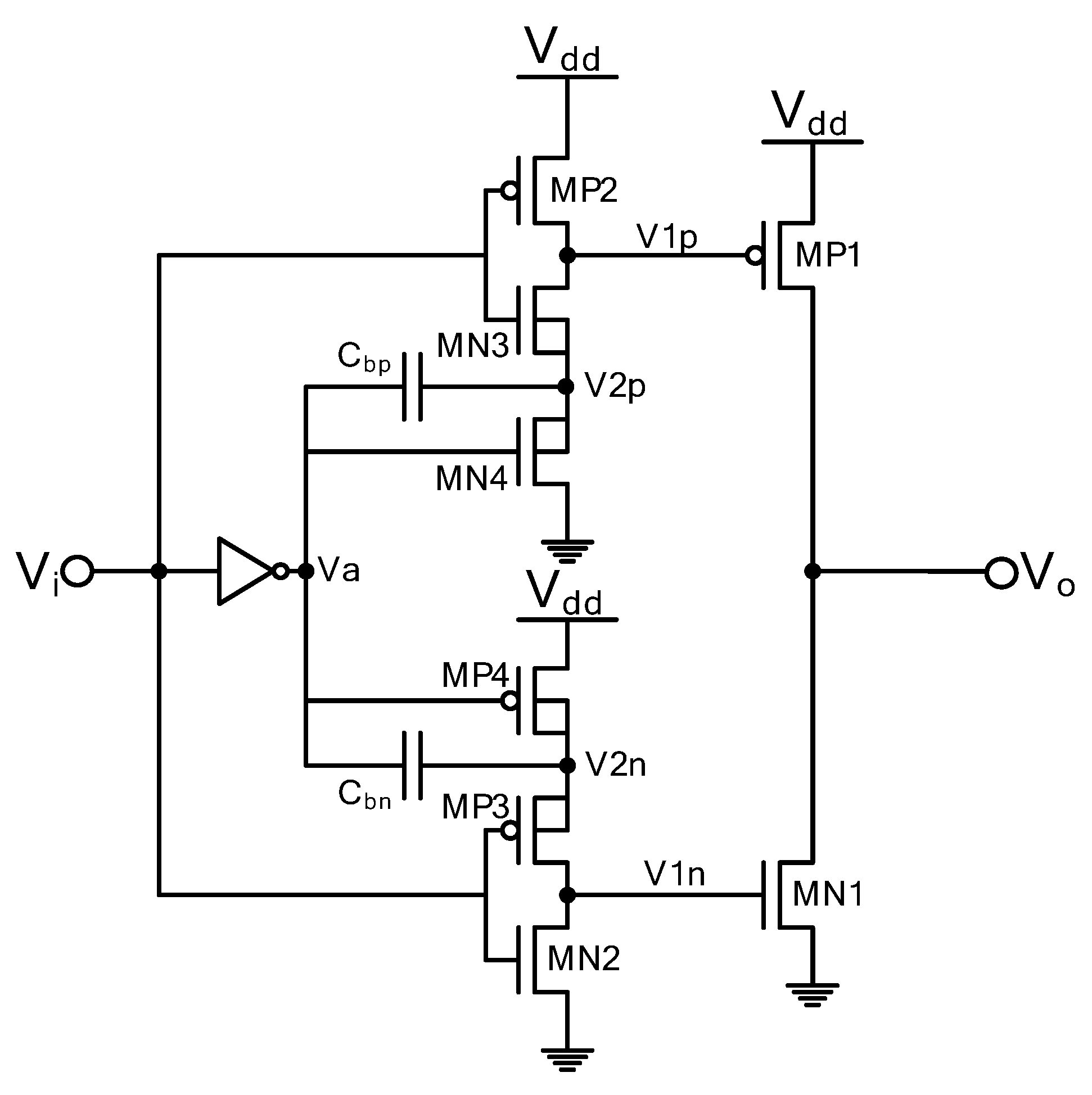
Figure 1.
Conventional bootstrapped CMOS driver [
3].
Figure 1.
Conventional bootstrapped CMOS driver [
3].
On the other hand, as the complexity of nanoscale CMOS VLSI grows, long interconnect metal lines and an output driver with a large distributed RC loading constrain the achievable performance. In order to drive a large distributed RC-load, the design of an energy efficient driver circuit has become a critical concern for switching speed and power consumption. Since the threshold voltage of a CMOS device cannot be easily scaled down with supply voltage, the design of an energy efficient high-performance driver operating at a low supply voltage (or subthreshold voltage level) poses a significant challenge [
3,
4,
5]. A bootstrapped CMOS driver circuit [
3] (shown in
Figure 1) was proposed previously. This driver mainly consists of positive and negative voltage bootstrapped circuits and a pair of corresponding driver transistors (MP1 and MN1). When the bootstrapped driver was functioning, gate nodes of driver transistors, V1n and V1p, were boosted above V
dd and below ground, respectively, to enhance the current driving ability of the driver transistors (MN1 and MP1), thus improving the switching speed of circuits with a large distributed RC loading. The enhanced current driving ability of the driver circuit is determined by the voltage levels of nodes V1n and V1p, which are boosted by two coupled capacitors, C
bn and C
bp, respectively. The extent of internal voltage undershoot (overshoot) of V1p (V1n) is determined by the ratio of C
bp (C
bn) to the parasitic capacitance at the right side of C
bp (C
bn), due to charge sharing. Ideally, by using large C
bp (C
bn), the boosted voltage level of V1p (V1n) can be pulled down (up) to near -V
dd (2V
dd). Thus, almost a -V
dd (2V
dd) voltage level is fed to the gate nodes of the driver transistor MP1 (MN1), respectively, providing a bootstrapping effect to enhance the driving capability.
Unfortunately, for the conventional bootstrapped CMOS driver in
Figure 1, even with a large boosting capacitor C
bp (C
bn), near −V
dd (2V
dd) voltage value cannot be generated and maintained at the corresponding gate node of the driver device, due to a leakage path through MN4 (MP4), which charges (discharges) node V1p (V1n). During the input-rising transition, V2p is boosted to below-ground voltage level (−V
dd), which is passed through an “On” transistor MN3 to node V1p to enhance the gate-drive of MP1. However, as V2p is over-driven to the below-ground level, a leakage current flows from the ground through MN4 (with its gate at the ground) to charge up V2p (and hence V1p), thus reducing/limiting the gate over-drive of MP1 and the boosting efficiency. The complementary situation occurs where the leakage path through the transistor MP4 discharges V2n (and hence V1n) during the input-falling transition.
In addition to the conventional bootstrapped driver, several bootstrapped driver designs have been reported [
6,
7,
8,
9,
10]. The bootstrapped driver designs in [
6] and [
7] utilize pre-charged capacitors to couple the output loading charges directly, thus incurring a large area overhead, as the capacitors have to be sized in proportion to the large output loading. The area overhead is exacerbated by the fact that a capacitor implemented with a MOS structure has quite a poor area efficiency (low capacitance per unit area) at a low voltage subthreshold operation. The bootstrapped CMOS driver in [
8] provides a short turn-on delay for faster speed. It, however, requires almost 2X transistor counts compared with the conventional bootstrapped driver in [
3] and has larger parasitic capacitance at the charge sharing gate nodes of the output driver devices, resulting in more power dissipation and degraded boosting efficiency. The bootstrapped driver in [
9] requires four capacitors, twice that of the conventional bootstrapped driver and, hence, a large area overhead. It also has a large cross-over current and, hence, a large power consumption. The conditional bootstrapped driver circuit in [
10] employs only one capacitor, but with two independent input signals to determine the state of the conditional output.
In this paper, an energy efficient bootstrapped CMOS driver is proposed to overcome the shortcomings of the conventional bootstrapped driver. The proposed succinct single-input to single-output scheme eliminates the leakage paths of the conventional scheme [
3] to prevent charging/discharging of the boosted nodes, thus enhancing the boosted voltage levels and allowing the boosted voltage levels to be maintained to enhance the boosting efficiency and switching speed. The proposed scheme requires an identical number (
i.e., two) of boosting capacitors and only four more transistors compared with the conventional bootstrapped driver in [
3]. In
Section 2, we describe the proposed bootstrapped driver circuit structure and its operation.
Section 3 presents the detailed test chip implementation in UMC 65 nm low-power CMOS technology.
Section 4 describes the testing environment, chip measurement results, and the measured performance comparison with the conventional bootstrapped driver. The conclusion of the paper is given in
Section 5.
2. Energy Efficient Bootstrapped Driver
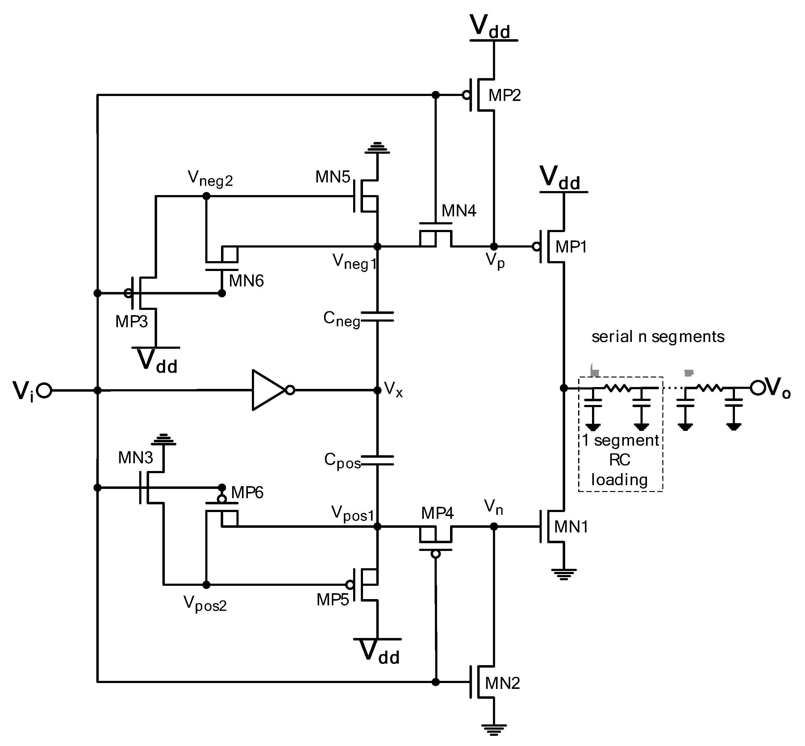
Figure 2 shows the proposed energy efficient bootstrapped CMOS driver [
11]. It consists of the basic driver block and the bootstrap block. In the basic driver block, there are PMOS (MP1) and NMOS (MN1) for pushing and pulling the output load. In the bootstrap block, there are two PMOS (MP2, MP3) and three NMOS (MN4, MN5, MN6) for push-up transient and two NMOS (MN2, MN3) and three PMOS (MP4, MP5, MP6) for pull-down transient. Moreover, two coupling capacitors (C
pos and C
neg) and one inverter are used for storing and coupling charges in the bootstrap block.
Notice that MN3, MN4 in the conventional driver (
Figure 1) and MN4, MN5 and MN6 in the proposed driver (
Figure 2) are shown with the source-body tied (V
SB = 0). In the following simulations and test chip implementation, the process used is the UMC 65 nm Low-Power (LP) CMOS process, a standard foundry bulk (PMOS in N-Well) process. So, the bodies of MN3, MN4 in the conventional driver and MN4, MN5 andMN6 in the proposed driver are tied to GND. As such, the body to source junctions of these NMOSs are reverse-biased (that raises V
T and reduces leakage).
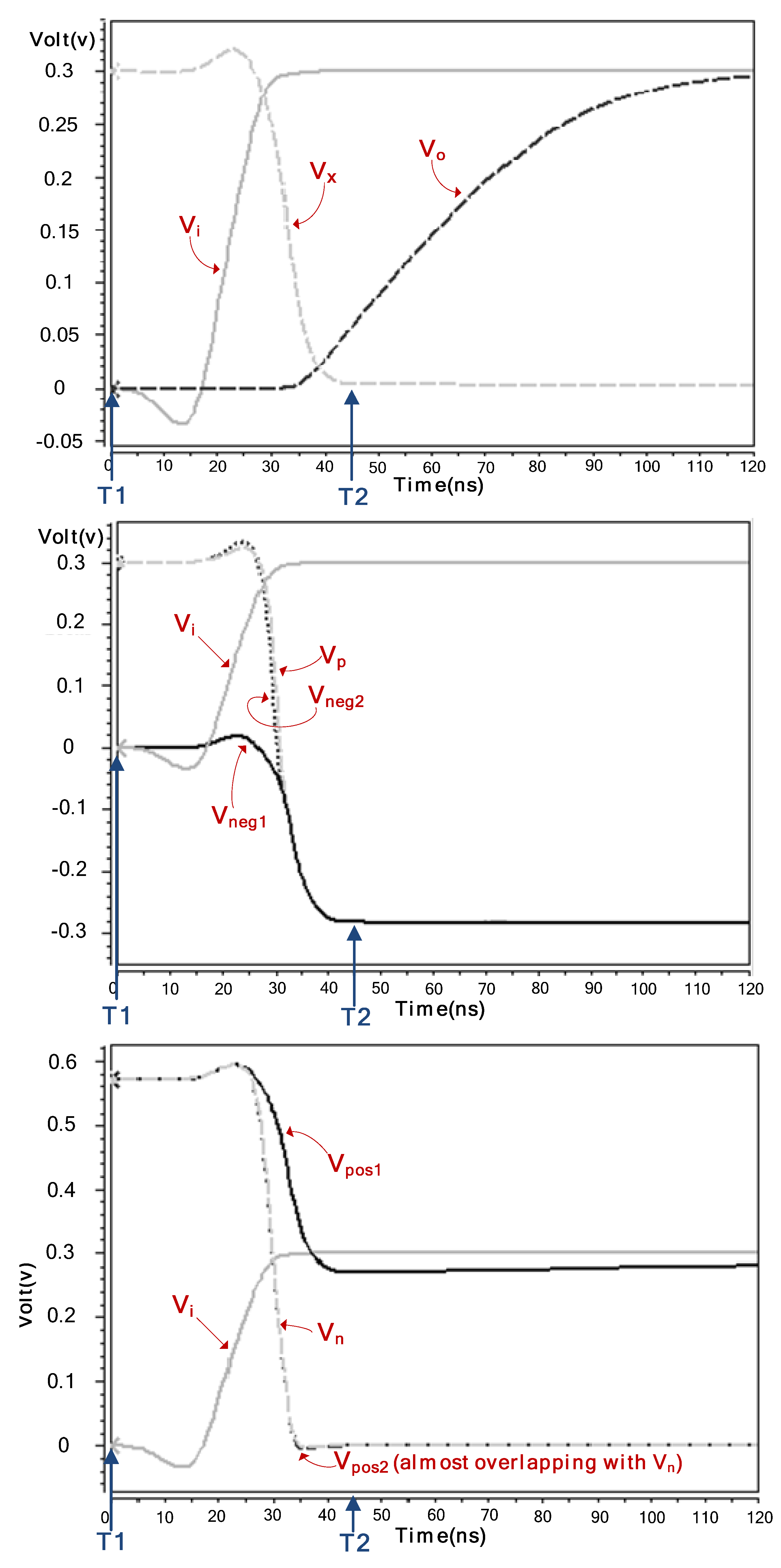
Figure 3 shows pertinent transient waveforms of the energy efficient bootstrapped driver, which drives a series of RC loading segments during the push-up transient. Note that the supply V
dd is set at 0.3 V for ultra low-voltage subthreshold operation. The driver circuit and RC loading segment are designed based on the UMC 65 nm low-power CMOS process. Each RC segment is composed of a 120 Ω resistor and two 504 fF capacitors, corresponding to 4 mm of M6 wire, extracted from a long metal wire in the 65 nm CMOS process. Fast push-up operation of the energy efficient bootstrapped driver is illustrated when the input rises from 0 V to 0.3 V.
Figure 2.
Proposed energy efficient bootstrapped CMOS driver.
Figure 2.
Proposed energy efficient bootstrapped CMOS driver.
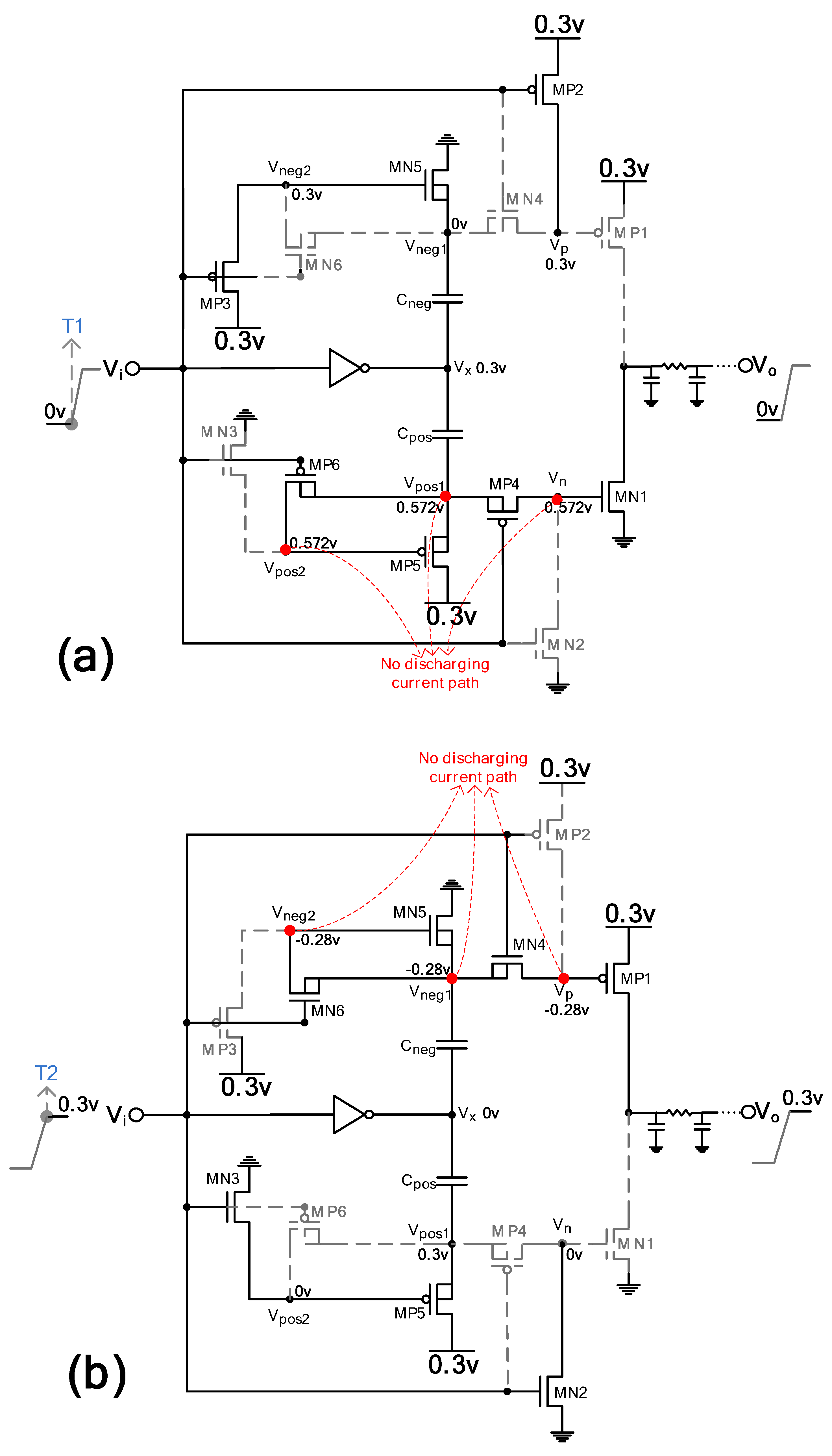
The equivalent driver circuit at time T1 before the push-up transient is shown in
Figure 4(a). At time T1, input V
i is at 0 V, and the output of the inverter, V
x, is at 0.3 V. Therefore, in the basic driver block, MP1 is off, and MN1 is on. In the bootstrap block, MN2, MN3, MN4 and MN6 are off and the rest transistors are on. Accordingly, the output node, V
o, is driven by MN1 to 0 V. The gate node of MN1, V
n, retains a high voltage because of the boosting of the V
pos1 node to nearly 0.6 V by C
pos and the fact that MP4 is on. Note that V
pos1 and V
n have been boosted in the preceding pull-down transient prior to the present push-up transient.
Notice also that there is no discharging current path from charge sharing nodes, Vpos1, Vpos2 and Vn. On the other hand, at T1, MP3 and MN5 of the bootstrap block are on, setting the top side of Cneg, Vneg1, to 0 V. As a result, the top and bottom side of the capacitor Cneg, Vneg1 and Vx are pre-charged to 0 V and 0.3 V, respectively. Therefore, at T1, capacitor Cneg has stored a charge of 0.3Cneg Coulombs.
Figure 3.
Pertinent push-up transient waveforms of an energy efficient bootstrapped CMOS driver at0.3 V.
Figure 3.
Pertinent push-up transient waveforms of an energy efficient bootstrapped CMOS driver at0.3 V.
Figure 4(b) illustrates the equivalent circuit of the energy efficient bootstrapped driver at time T2 after the push-up transient. At T2, the input V
i has ramped up to 0.3 V. MP3 and MP2 are off. MN6 and MN4 turn on, and the output of the inverter V
x is pulled down to 0 V. The top side of bootstrap capacitor C
neg (V
neg1) is coupled from 0 V to near -0.3 V. As MN6 and MN4 are on at T2, V
p and V
neg2 are also coupled to near −0.3 V, thus providing under-drive to enhance the driving capability of MP1, while simultaneously cutting off the leakage current path through MN5 by equalizing voltages of V
neg1 and V
neg2. The pertinent waveforms for the push-up transient are shown in
Figure 3. The pull-down bootstrap transient operates in a complementary manner.
Table 1 lists the bootstrapped device states of the proposed Energy Efficient (EE) driver and the Conventional (Conv.) driver in the rising and falling transients in detail. It can be seen that MN4 (MP4) in the conventional driver has a large V
gs (V
sg)~V
DD during the boosting transient, thus causing significantly higher leakage than the proposed EE driver.
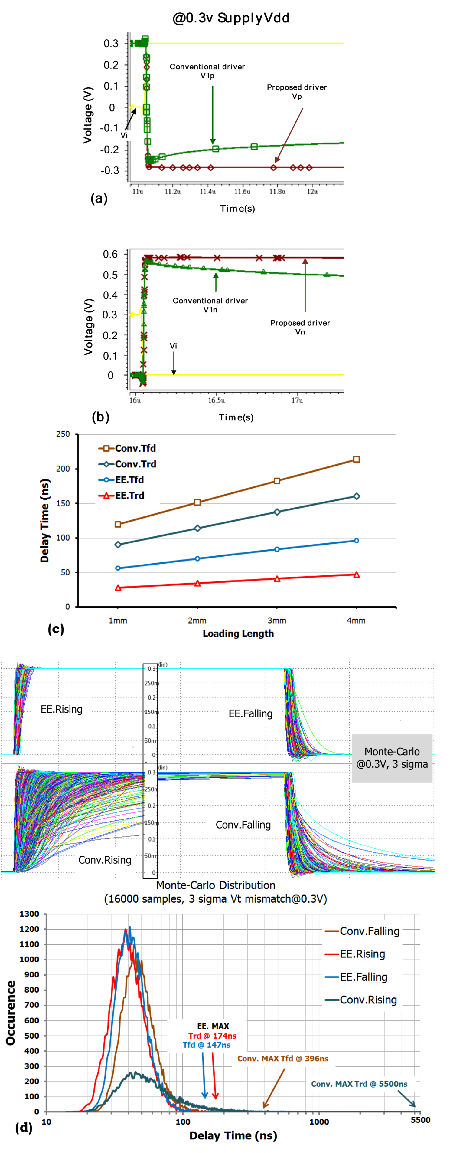
Figure 5(a,b) shows the waveforms of boosted node voltages (V1n and V1p of the conventional bootstrapped driver and V
n and V
p of the proposed driver) at V
dd = 0.3 V, 25 °C, TT corner. V
n (V
p) of the proposed driver is boosted to a higher (lower) voltage level than V1n (V1p) of the conventional driver. The decaying of the voltage levels of V1n and V1p due to leakage paths through MP4 and MN4 (discussed early in
Section I) can be seen.
Figure 5(c) compares the delays of the conventional driver and the proposed driver for wire length ranging from 1 mm to 4 mm. The performance advantage of the proposed driver can be clearly seen across this loading range.
Monte-Carlo simulations with 16,000 samples for three sigma Vt mismatch are performed. The results for the delay distributions of the conventional driver and the proposed driver at 0.3 V are shown in
Figure 5(d). It can be seen clearly that the proposed driver offers better performance and tighter delay distribution.
Figure 4.
Equivalent circuit of energy efficient bootstrapped CMOS driver during the push-up transient period (a) at time T1; (b) at time T2.
Figure 4.
Equivalent circuit of energy efficient bootstrapped CMOS driver during the push-up transient period (a) at time T1; (b) at time T2.
Table 1.
Bootstrapped device states of the proposed Energy Efficient (EE) driver and the Conventional (Conv.) driver in rising and falling transients, respectively.
Table 1.
Bootstrapped device states of the proposed Energy Efficient (EE) driver and the Conventional (Conv.) driver in rising and falling transients, respectively.
| Bootstrapping Comparison | Device State | NMOS Vgs/PMOS Vsg | |Vds| |
|---|
| Conv. (Rising) | MN4 (turn ON) | ![Jlpea 02 00282 i001]() | ≈VDD > 0 |
| MP2 (turn OFF) | Vsg ≈ −2VDD < 0 |
| Conv. (Falling) | MP4 (turn ON) | ![Jlpea 02 00282 i002]() | ≈VDD > 0 |
| MN2 (turn OFF) | Vgs ≈ −2VDD < 0 |
| EE. (Rising) | MN5 (turn OFF) | Vgs = 0 | ≈VDD > 0 |
| MP2 (turn OFF) | Vsg ≈ −2VDD < 0 |
| MP3 (turn OFF) | Vsg ≈ −2VDD < 0 |
| EE. (Falling) | MP5 (turn OFF) | Vsg = 0 |
| MN2 (turn OFF) | Vgs ≈ −2VDD < 0 |
| MN3 (turn OFF) | Vgs ≈ −2VDD < 0 |
Figure 5.
Waveforms of bootstrapped node voltages during (a) push-up and (b) pull-down transients (V1n and V1p of the conventional bootstrapped driver and Vn and Vp of the proposed driver) at supply Vdd = 0.3 V, 25°C, TT corner; (c) performance evaluation of 50% to 50% delay times vs. loading wire ranging from 1 mm to 4 mm length; (d) Monte-Carlo simulation results with three sigma VT mismatch at 0.3 V, 16000 samples.
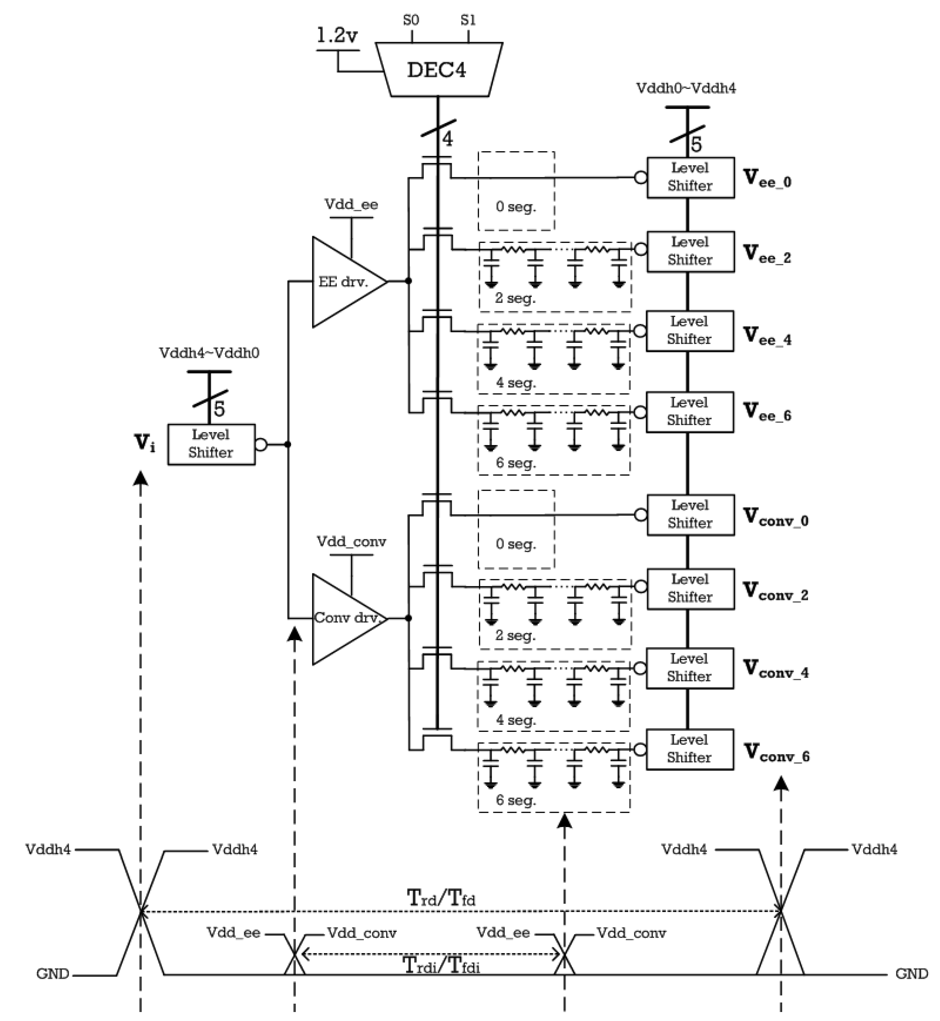
3. Test Chip Implementation
A test chip is designed in UMC 65 nm low-power CMOS technology for performance evaluation and comparison with the conventional bootstrapped driver. The test chip structure is shown in
Figure 6. The input Level Shifter [
12] down-shifts the normal (high) voltage input to the desired low-voltage for the driver input. The voltage down-shift is performed in five successive steps with five power domains to mitigate ESD reliability issues between power domains with large voltage disparity. The output of the Level Shifter is fed to the proposed energy efficient driver and the conventional bootstrapped driver. Four NMOS-only pass-transistor based multiplexer switches are provided at the output of each driver to allow selection of four different loading segments of 0 mm, 8 mm, 16 mm and 24 mm long M6 metal line, respectively. The signals at the far-end of the loading segments are then up-shifted by the output Level Shift, again, in five successive steps with five power domains, to the normal (high) voltage. The successive down/up-shift with multiple power domains not only alleviates ESD reliability issues between power domains with large voltage disparity, but also provides a better shift-voltage level control under Process, Voltage and Temperature (PVT) variation. The decoder of the NMOS-only pass-transistor-based multiplexer operates at the standard high voltage domain to over-drive the pass-transistor, so the V
T loss through the NMOS-only pass-gate and the multiplexer delay are negligible.
Figure 6.
Test chip structure for driver comparison in UMC 65 nm CMOS technology.
Figure 6.
Test chip structure for driver comparison in UMC 65 nm CMOS technology.
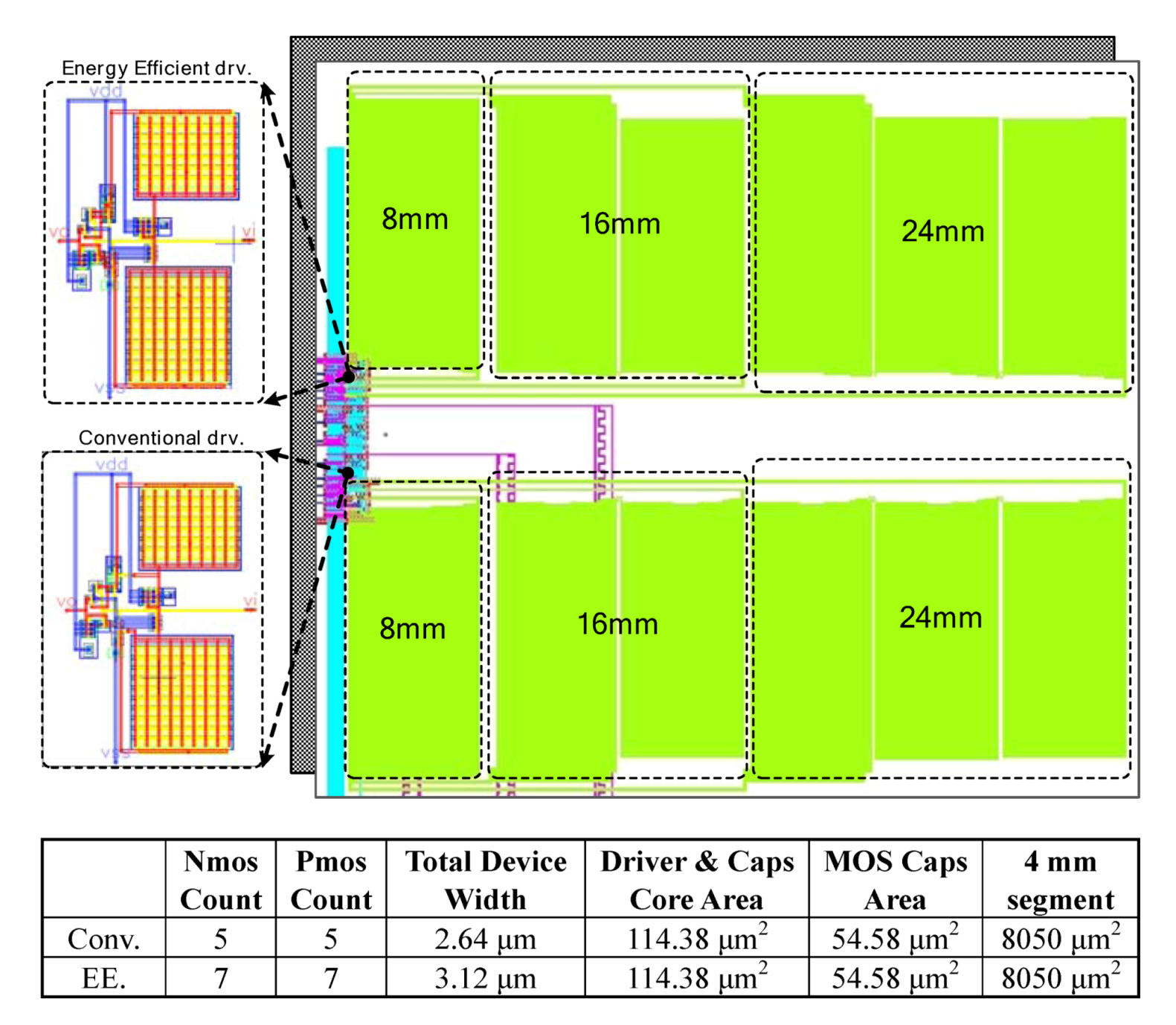
Figure 7 shows the layout view of the test chip and the table summarizes the device count, total device width, MOS coupling cap area and core area of the conventional driver and the proposed energy efficient driver. The proposed energy efficient bootstrapped driver is located at the upper-half, while the low-half is the conventional bootstrapped driver. The 8 mm, 16 mm and 24 mm loading segments are drawn by folding M6 metal lines. The insets show the blow-up views of the relatively small bootstrapped driver blocks, where the two boosting capacitors for each driver can be clearly seen. While the proposed driver has a higher device count, the space between N-wells for the PMOS capacitor could accommodate the extra devices, resulting in an identical area compared with the conventional driver.
In the energy efficient and the conventional bootstrapped drivers, all transistors, except MP1, of
Figure 1 and
Figure 2 have a minimum length and width. MP1 has a minimum length, and the width is three times larger than the minimum width. The MOS-based capacitances of C
neg(C
bp) and C
pos(C
bn) in
Figure 2 (
Figure 1) are 40 fF and 30 fF, respectively. The inverter in both figures is composed of a PMOS with a minimum length and nine times minimum width and an NMOS with a minimum length and three times minimum width. The test chip is designed and taped out in UMC 65 nm low-power CMOS technology.
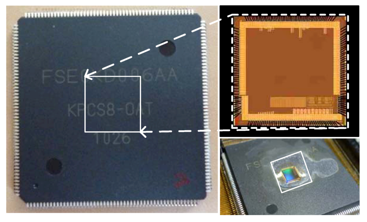
Figure 8 shows the packaged test chip and the internal transection screen within the QFP208-type package.
Figure 7.
Test chip layout view with four types of loading segments of 0 mm, 8 mm, 16 mm and 24 mm long M6 metal lines, respectively. The table shows comparisons of the device count, total device width, MOS coupling cap area and core area of the conventional driver and the proposed energy-efficient driver.
Figure 8.
Quad Flat Packaged test chip and transection screen within the chip package.
Figure 8.
Quad Flat Packaged test chip and transection screen within the chip package.
4. Measurement and Performance Evaluation
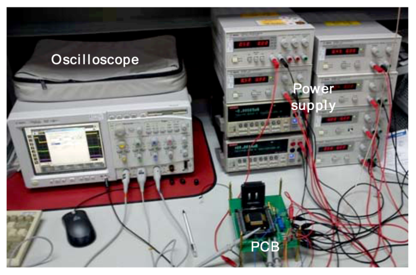
Figure 9 shows the measurement environment setup, including oscilloscope, PCB and multiple power supplies. A 50% duty-cycle clock signal is supplied to the input of the test chip.
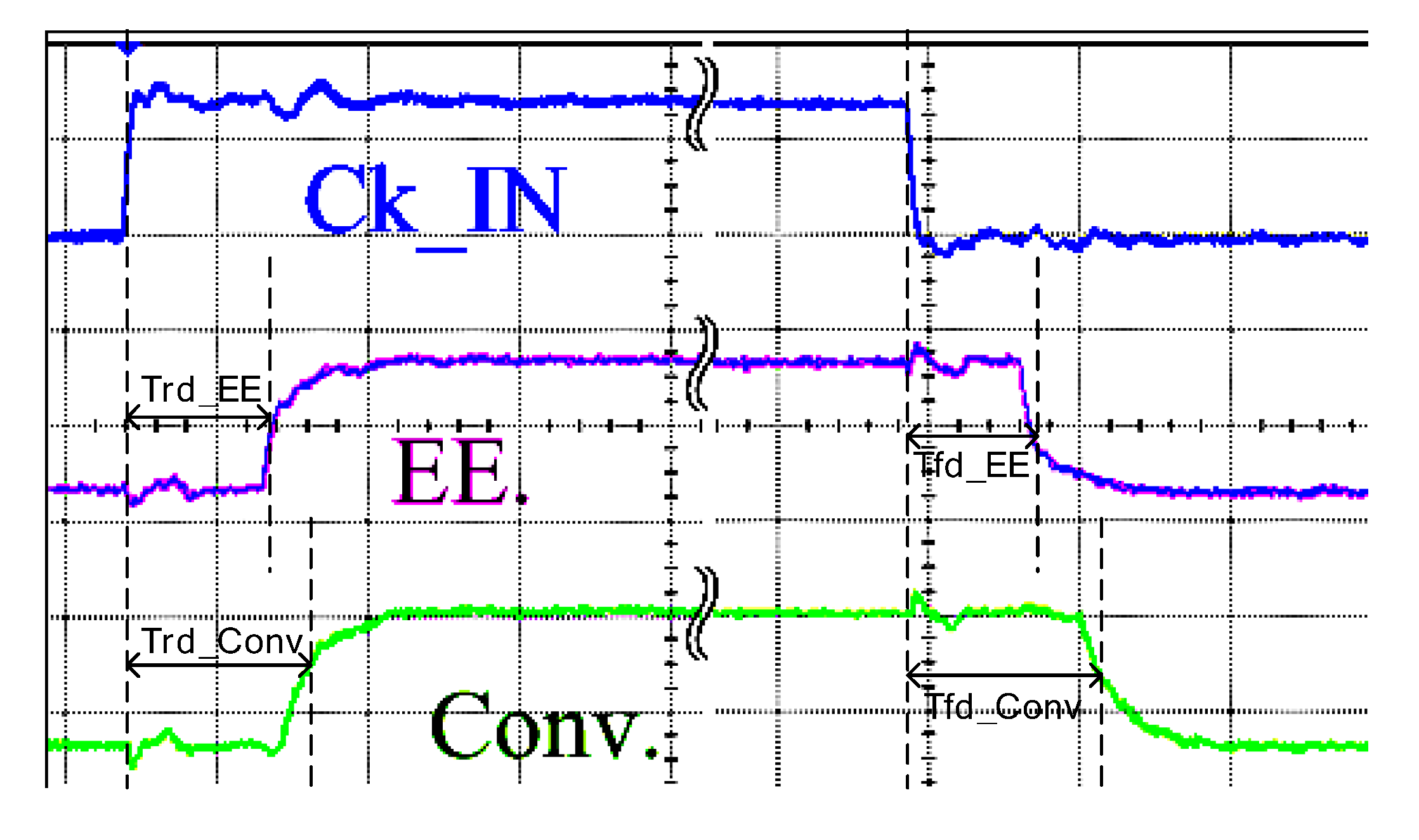
Figure 10 shows the pertinent measured oscilloscope waveforms, including the input (CK_IN) signal and two of the eight output signals (selected by the 2-bit multiplexer, one output for each driver scheme as shown in
Figure 6) for the Energy Efficient (EE.) driver and the Conventional (Conv.) bootstrapped driver. The 50% to 50% rising and falling delay times (Trd and Tfd) from the input to output are measured. Notice that Trd and Tfd are “external” delays, which include the delays of the input and output level shifters, so we have to deduct the delays of the level shifters to obtain the “internal” delays (shown as Trdi and Tfdi in
Figure 6), which represent the true delays from the driver input to the far end of the load. Separate power supply pins are used for each type of driver, so the power consumption of each driver can be measured precisely.
Figure 9.
Test chip measurement setup with oscilloscope, PCB and multiple power supplies.
Figure 9.
Test chip measurement setup with oscilloscope, PCB and multiple power supplies.
Figure 10.
Measured oscilloscope waveforms; Top: Input (CK_IN) signal; Middle: Output from Energy Efficient (EE.) driver; Bottom: Output from Conventional (Conv.) bootstrapped driver.
Figure 10.
Measured oscilloscope waveforms; Top: Input (CK_IN) signal; Middle: Output from Energy Efficient (EE.) driver; Bottom: Output from Conventional (Conv.) bootstrapped driver.
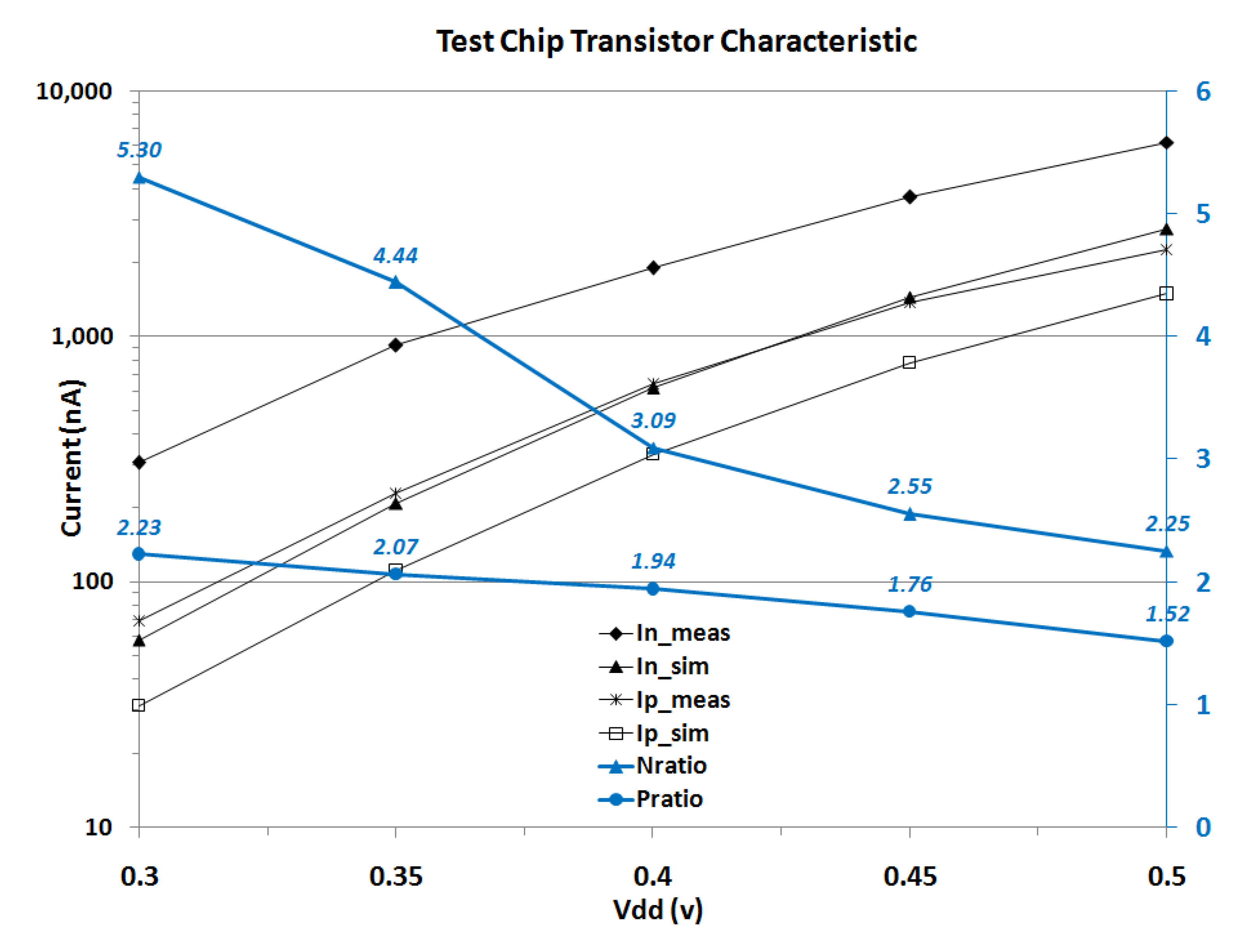
Figure 11.
Simulated and measured N/ PMOS transistor on-current vs. VDD.
Figure 11.
Simulated and measured N/ PMOS transistor on-current vs. VDD.
Figure 11 shows the post-simulation and measured on-current of NMOS and PMOS transistor
versus supply voltage ranging from 0.3 V to 0.5 V. As can be seen, for both NMOS and PMOS, the measured on-current is much larger than the post-simulation results. The data of blue lines (Nratio and Pratio) corresponding to the right Y-axis represent the ratio of the measured on-current to the post-simulation on-current. It is obvious that the test chip devices have larger current driving capability than the post-simulation results based on the device models. The discrepancy becomes larger with lower supply voltage. This is attributed to the fact that the device models from the foundry are typically well-calibrated only for operation in the super-threshold region (e.g., say 0.7–1.2 V), and not for operation in the subthreshold region, and the large variability of device characteristics in the subthreshold region.
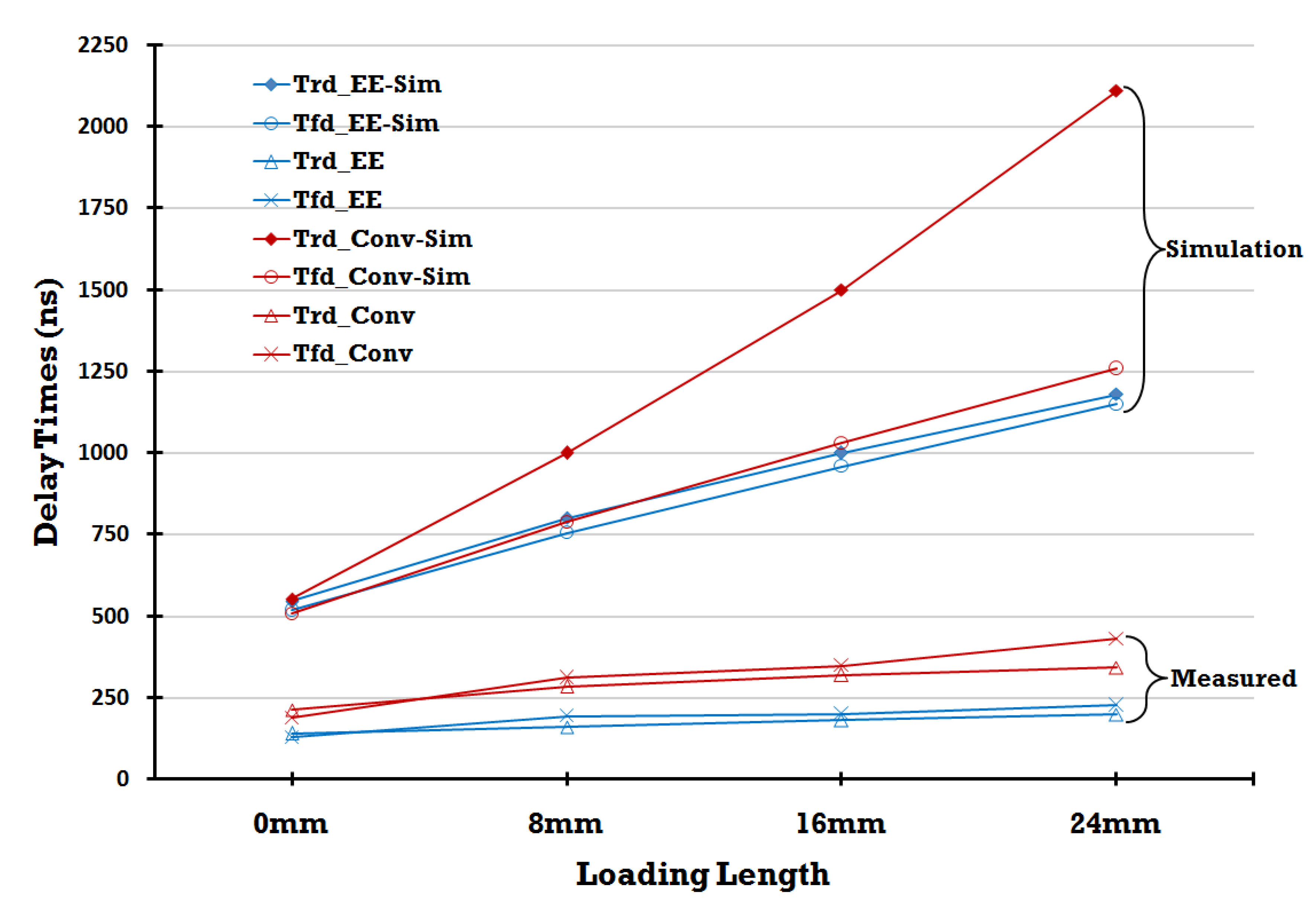
Figure 12 shows the post-simulation and the measured “external” rising and falling delay times (Trd and Tfd) at 0.3 V supply. The smaller delays of the measured results are due to the significantly larger device current driving capability than that predicted by the device models as shown in
Figure 11.
Figure 12.
External delay times (Trd and Tfd ) of energy efficient and conventional bootstrapped drivers at 0.3 V supply vs. M6 wire loading length. Both post-simulation and measured results are shown.
Figure 12.
External delay times (Trd and Tfd ) of energy efficient and conventional bootstrapped drivers at 0.3 V supply vs. M6 wire loading length. Both post-simulation and measured results are shown.
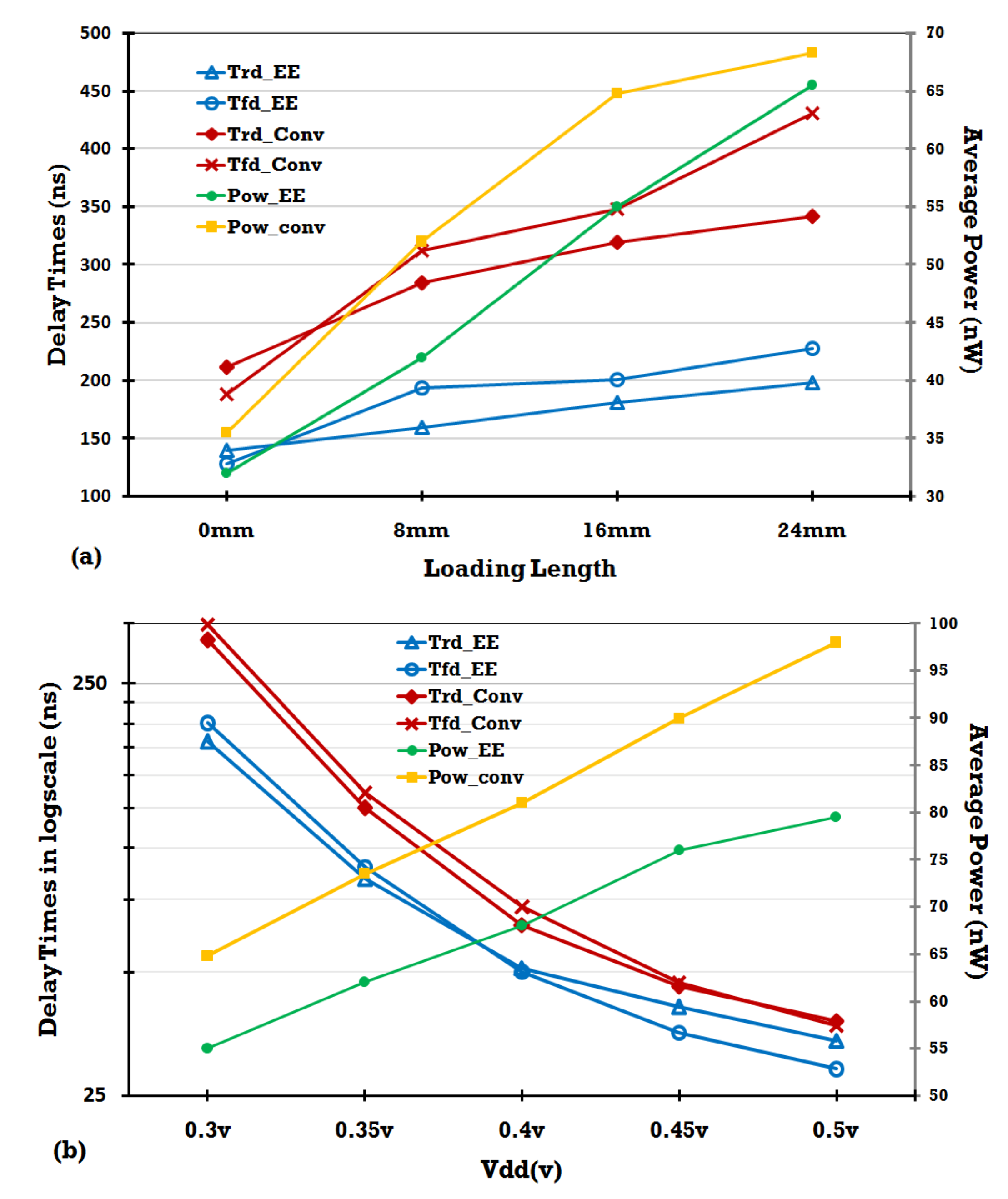
Figure 13(a) shows the measured “external” rising and falling delay times and average power consumption of the Energy Efficient (EE.) and Conventional (Conv.) bootstrapped driver circuit
versus the M6 wire loading length at 0.3 V.
Figure 13(b) shows the measured “external” rising and falling delay times and average power consumption of the Energy Efficient (EE.) and Conventional (Conv.) bootstrapped driver circuit
versus V
DD with a loading of 16 mm M6 wire.
As mentioned previously, Trd and Tfd are “external” delays, which include the delays of the input and output level shifters, and we have to deduct the delays of the level shifters to obtain the “internal” delays Trdi and Tfdi. Notice that if one simply constructs a path (chain) consisting of only the input level shifters and output level shifters, the so-obtained level shifter delay does not represent the actual situation, since in
Figure 6, the last stage of the input level shifters is driving the proposed or conventional bootstrapped driver, whereas in the level shifter chain, it is driving the first stage of the output level shifters.
Similarly, in
Figure 6, the input of the first stage of the output level shifters is driven by the far end of the M6 loading wire, while in the level shifter chain. it is driven by the last stage of the input level shifters. If the device models were accurate, one could also rely on post-simulations to obtain the delays of the level shifters and deduct them from the “external” delays. However, given the large discrepancy for on-currents between the post-simulation results and measured hardware results shown in
Figure 11 (and the large discrepancy between the “external” delays from post-simulations and measured hardware results in
Figure 12), direct deduction of post-simulation level shifter delays from the measured “external” delays would yield inaccurate (and even meaningless) data.
Figure 13.
Measured external delay times (Trd and Tfd) and average power consumption of Energy Efficient (EE.) and Conventional (Conv.) bootstrapped drivers versus (a) M6 wire loading length at 0.3 V; (b) VDD with 16 mm long M6 wire.
Figure 13.
Measured external delay times (Trd and Tfd) and average power consumption of Energy Efficient (EE.) and Conventional (Conv.) bootstrapped drivers versus (a) M6 wire loading length at 0.3 V; (b) VDD with 16 mm long M6 wire.
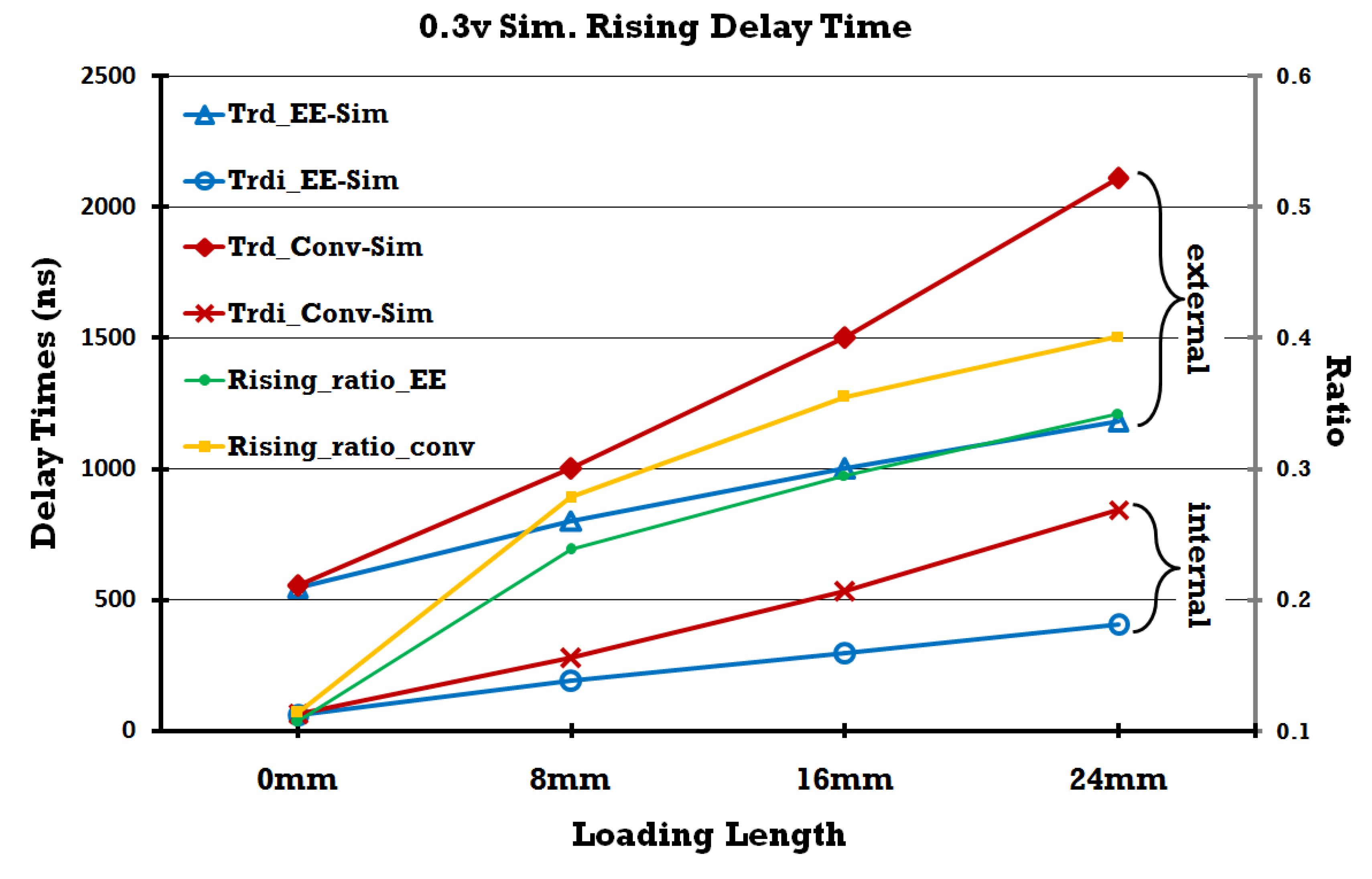
Figure 14.
Simulated internal (Trdi) and external (Trd) rising delay times and internal to external rising delay ratio (Trdi/Trd) of Energy Efficient (EE.) and Conventional (Conv.) bootstrapped drivers versus M6 wire loading length at 0.3 V.
Figure 14.
Simulated internal (Trdi) and external (Trd) rising delay times and internal to external rising delay ratio (Trdi/Trd) of Energy Efficient (EE.) and Conventional (Conv.) bootstrapped drivers versus M6 wire loading length at 0.3 V.
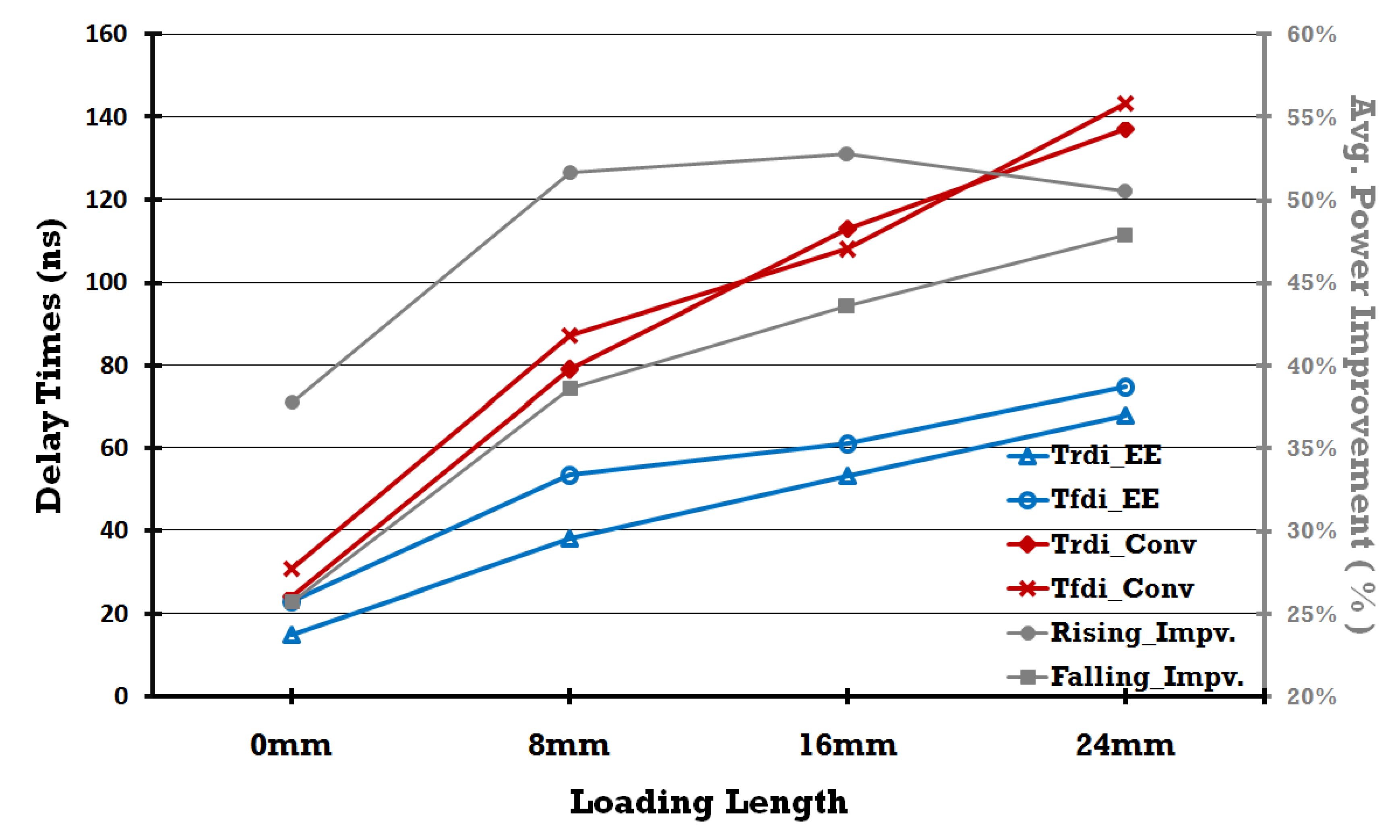
Figure 15.
Deduced internal delays (Trdi and Tfdi) from measured external delays (Trd and Tfd) at 0.3 V and rising and falling delay improvement (in %) of proposed energy efficient driver with respect to conventional bootstrapped driver vs. M6 wire loading length
Figure 15.
Deduced internal delays (Trdi and Tfdi) from measured external delays (Trd and Tfd) at 0.3 V and rising and falling delay improvement (in %) of proposed energy efficient driver with respect to conventional bootstrapped driver vs. M6 wire loading length
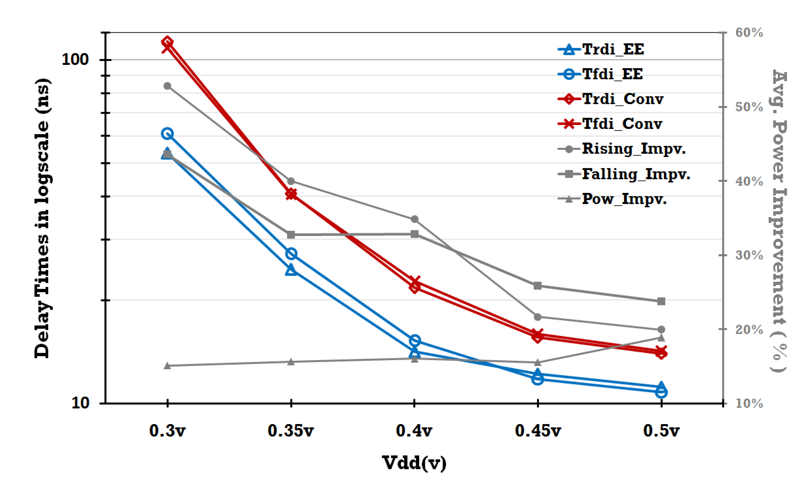
Figure 16.
Deduced internal delays and average power improvement vs. VDD with 16 mm long M6 wire of the proposed energy efficient driver with respect to conventional bootstrapped driver.
Figure 16.
Deduced internal delays and average power improvement vs. VDD with 16 mm long M6 wire of the proposed energy efficient driver with respect to conventional bootstrapped driver.
In order to obtain reasonable estimates of the level shifter delays (hence “internal” delays Trdi and Tfdi), we calculate the ratio of “internal” delays to “external” delays based on post-simulation results (as shown in
Figure 14) and then apply the ratio to the measured “external” delays to obtain the “internal” delays. The deduced “internal” delays, together with the rising and falling delay improvement (in %) of the proposed energy efficient driver with respect to the conventional bootstrapped driver
vs. M6 wire loading length, are shown in
Figure 15.
As can be seen from
Figure 15, the proposed driver provides (“internal”) a rising-delay improvement of 37%–50% and (“internal”) a falling-delay improvement of 25%–47% at 0.3 V for loading ranging from 0 to 24 mm long M6 metal line.
Figure 16 shows the deduced “internal” rising and falling delay times and average power improvement of the Energy Efficient (EE.) driver with respect to the Conventional (Conv.) bootstrapped driver
versus V
DD with a loading of 16 mm M6 wire. Although designed and optimized for subthreshold ultra low-voltage operation, the proposed bootstrapped driver can be seen to be advantageous at higher nearly-threshold supply voltage (0.5 V) as well. The proposed driver provides “internal” rising delay improvement of 20% to 52% and falling delay improvement of 23%–43% for V
DD ranging from 0.3 V to 0.5 V, while driving 16 mm long M6 wire. Furthermore, the proposed driver consumes about 15% less average power (at higher speed) than the conventional bootstrapped driver for the same supply voltage range.


